DOI:
10.1039/D0MA00258E
(Paper)
Mater. Adv., 2020,
1, 1186-1192
Bond states, moiré patterns, and bandgap modulation of two-dimensional BN/SiC van der Waals heterostructures†
Received
29th April 2020
, Accepted 22nd June 2020
First published on 22nd June 2020
Abstract
The matched lattice strain of the graphene/hexagonal boron nitride (BN) heterojunction that is less than 2% is known to form a moiré pattern. However, in the BN/SiC heterojunction, the formation of a moiré pattern for a lattice strain more than 5% is a novel phenomenon. This study aims to determine moiré patterns on the BN/SiC heterojunction at lattice strains of 5% and 7% and different incident angles, which can be applied to photoelectric detection technology. The BN/SiC-1 and BN/SiC-2 heterojunctions formed in this study had bandgaps of 0.851 and 1.373 eV, respectively. Furthermore, we observed that when two BN/SiC heterojunctions have indirect bandgaps, the BN/SiC van der Waals heterojunction can be a potential photoelectric material. We analyze the bonding states using the bond-charge model and calculate the potential functions of the antibonding, bonding, and nonbonding states. This study provides a theoretical reference for the precise regulation of the charge density and chemical bonding states of the 2D material surface.
1. Introduction
The successful preparation of a two-dimensional (2D) atomic layer of the planar graphene structure has encouraged researchers to investigate 2D nanomaterials.1–4 Owing to the similarities between the structures and bonding properties of hexagonal boron nitride (BN) and graphite, shortly after the preparation of graphene, a single layer of hexagonal honeycomb BN was successfully prepared by micromechanical stripping.5 BN has a layered hexagonal honeycomb structure with a wide band gap of 4.6 eV.6 However, to increase the efficiency of light absorption and convert the 2D hexagonal BN sheet to a highly efficient photocatalytic material, the band gap of BN needs to be reduced to approximately 1.5 eV.7 Hu et al. found that the band gap can be reduced through lattice strain regulation of the BN sheet.8 Tang et al. found that band gap reduction can be achieved through electric field regulation of the BN sheet.9 He et al. achieved the regulation of electronic structures in two-dimensional transition metal-doped BN materials through hydrogen and fluorine chemical modification.10 These studies provide the theoretical references for band gap regulation.
When manufacturing electronic devices, the majority of the 2D materials are grown on metals or semiconductor substrates, which causes strain in the crystal lattice.11–13 There exists a difference of 1.84% between the lattice constants of graphene and hexagonal BN.14 Additionally, the graphene/hexagonal BN system forms a moiré pattern.15,16 Furthermore, Kang et al. studied the 2D MoS2/MoSe2 heterojunction and found that the strength of the van der Waals interaction between the MoS2 and MoSe2 layers is not sufficient to eliminate this mismatch resulting in lattice strain. Zhang et al. studied the interlayer couplings, moiré patterns, and 2D electronic superlattices in MoS2/WSe2 hetero-bilayers.17 Rosenberger et al. studied the moiré pattern of a transition metal dichalcogenide heterostructure and found that the angle rotation is related.18 Cao et al. found that the superconducting properties of two layers of graphene were exhibited at specific angles (approximately 1.1°).19 Therefore, matching lattice strains of interlayer couplings and angle rotation of the two atomic layer heterojunctions will form a moiré pattern.20 The formation of the moiré pattern has led to the emergence of many novel physical and chemical properties.21–24
In this study, we found that lattice strains of 5% and 7% will cause a moiré pattern on the BN/SiC heterojunctions. The band gaps of BN/SiC-1 and -2 heterojunctions are approximately 0.851 and 1.373 eV, respectively. Furthermore, these heterostructures effectively modulate the bandgaps of BN (4.661 eV) and SiC (2.108 eV). This provides a basis for designing 2D semiconductor heterojunction materials, where the lattice strain can be controlled in different directions to regulate the band gap. Furthermore, we calculate the potential of the antibonding, bonding, and nonbonding functions using the bond-charge (BC) model, which provides a theoretical reference for the precise regulation of the charge density and chemical bonding states of the 2D material surface.
2. Principles
2.1 DFT calculations
The two-dimensional material geometry structure was obtained from the crystal Material Projects database. Then, through the interface function of the QuantumWise's software, structural models of the heterojunction (∼30–50 kinds of possible structures) are established, and the lattice strain value that matches the geometry structure from the database is the obtained lattice strain. The model of the initial structure only considers the lattice strain of the BN atomic layer. The average strain in the BN layer is listed in Table 1. The initial structure is geometrically optimized in the Vienna ab initio simulation package, and the relaxation model includes optimization of atomic positions and unit cells. We set the energy cut off of the plane wave at 400 eV and the Brillouin zone at 4 × 4 × 4 k-points. To acquire the optimized geometric structures, the energy convergence criterion is 10−5 eV, and the atomic force convergence is 0.01 eV Å−1. Next, the Cambridge Sequential Total Energy Package (CASTEP) was used to optimize the geometry and increase the accuracy of calculating chemical bonding and electronic properties.
Table 1 (a) Angles and lattice parameters of the BN/SiC heterostructures. (b) Corresponding set values of k-points, cut off, and lattice strain ε of the BN/SiC heterostructures
| (a) |
|
|
Angles |
Lattice parameters |
| Structures |
α (°) |
β (°) |
γ (°) |
A (Å) |
B (Å) |
C (Å) |
| BN/SiC-1 |
90 |
90 |
90 |
5.36 |
6.19 |
24.93 |
| BN/SiC-2 |
90 |
90 |
109.11 |
5.36 |
8.19 |
25.93 |
| (b) |
|
|
k-points |
Cut off (eV) |
ε
11 (%) |
ε
22 (%) |
ε
12 (%) |
ε (%) |
| BN/SiC-1 |
10 × 9 × 2 |
700 |
6.65 |
−5.20 |
10.26 |
7.37 |
| BN/SiC-2 |
10 × 6 × 2 |
700 |
6.65 |
−11.12 |
0.00 |
5.93 |
The DFT calculations, using the norm-conserving potentials of the hybrid density functional, were implemented in the CASTEP software. We use the Heyd–Scuseria–Ernzerhof (HSE06)25 hybrid density functional to describe the electron exchange and correlation potential. There are no constraints on the atomic layer. Also, we consider non self-consistent dipole correction in the calculation process. The thickness of the vacuum region is 14 Å. The energy convergence criterion is set to 1 × 10⁻⁶ eV, and the plane wave cut-off energy is set to 700 eV. To consider the long-range van der Waals interaction, we use the TS scheme for DFT-D calculation. Table 1 summarizes the parameters used in the DFT calculations.
2.2 BOLS-BC model
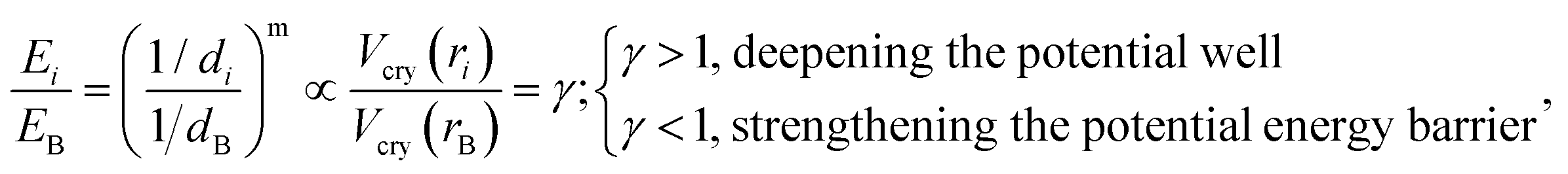
The following equations are used to describe the electronic state of a specific chemical bond, based on the bond-order–length–strength (BOLS) notation:26| |  | (1) |
where di is the bond length of the atom, Ei represents the single bond energy, Vcry(ri) is the crystal potential, m is the bond nature, B represents bulk atoms, and i counts from the outermost atomic layer inward up to the third indicator layer (i ≤ 3).
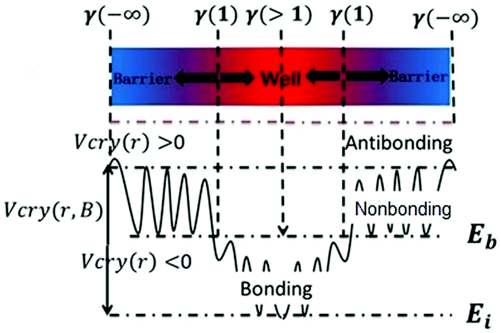
Eqn (1) describes the relationship between the chemical bonds (energy and length) and crystal potential functions based on the BOLS notation.27 The potential function γ Vcry (ri) may become deeper (γ > 1 for potential well formation) or shallower (γ < 1 for potential barrier formation) than the corresponding Vcry (rB) of the specific constituent.28
| |  | (2) |
Eqn (2) describes the relationship between the bond energy Ei, crystal potential Vcry(ri), bandgap EG, and the deformation charge density Δρ(ri). Fig. 1 illustrates the BC model with the BOLS notation.
 |
| | Fig. 1 Schematic of the bond-charge (BC) model in combination with the BOLS notation. | |
3. Results and discussion
3.1 Geometry structure
The geometry structure of the different strains is selected based on QuantumWise's interface modeling, and the geometry structure to be optimized is obtained. The lattice strain (>5%) produces the BN/SiC heterostructures (orthorhombic (Fig. 2a and c) or rhombohedral (Fig. 2b and d)). Fig. 2c and d show that both BN/SiC-1 and BN/SiC-2 heterojunctions form a wave-shaped geometry structure. The optimized heterostructures 1 and 2 are depicted in Table 1. We calculate the total energy of the BN, SiC, and BN/SiC stable structures, and the energy difference between them is calculated as the formation energy,29 using the equation Eform = Eheterostructuretotal − ESiCtotal − EBNtotal, as presented in Table 2. The formation energies of the two BN/SiC heterojunctions 1 and 2 are −1.26 and −1.16 eV, respectively, and these values are within the range of our calculation accuracy. Therefore, we confirm that both structures are stable with BN/SiC heterojunctions.
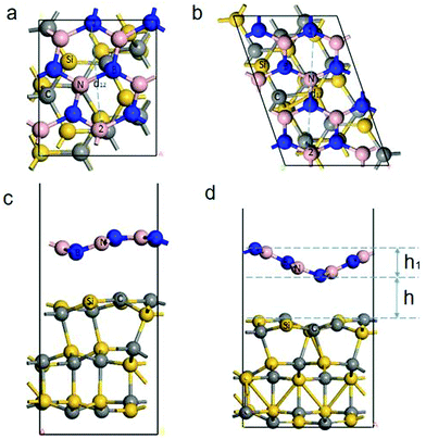 |
| | Fig. 2 (a) and (b) Top views of the BN/SiC-1 and 2 heterostructures. (c) and (d) Side views of the BN/SiC-1 and 2 heterostructures. The height (h) between the BN and SiC layers is the distance between the BN and SiC layers in the thickness direction of the slab. The height h1 is the height of the wave shape structure of heterostructures 1 and 2. The distance d12 is the distance between atom 1 and atom 2 of heterostructures 1 and 2. | |
Table 2 The formation energy Eform = Eheterostructuretotal − ESiCtotal − EBNtotal of BN/SiC-1 and BN/SiC-2 heterostructures
|
E
heterostructuretotal (eV) |
E
SiCtotal (eV) |
E
BNtotal (eV) |
E
form(eV) |
| BN/SiC-1 |
−5232.97 |
SiC |
−3142.01 |
BN |
−2089.70 |
−1.26 |
| BN/SiC-2 |
−6720.69 |
SiC |
−3927.88 |
BN |
−2791.65 |
−1.16 |
Additionally, we obtain the wave shape height h1 of the BN layer, as presented in Table 3 and Fig. 2. The height (h) between the BN and SiC layers is the distance between the BN and SiC layers in the thickness direction of the slab. We calculate the different initial heights (H) between the BN and SiC layers, and atomic distance of the BN layer, as shown in Table 4. The relaxation heights h for the BN and SiC heterostructures are 2.43 Å and 2.73 Å, respectively. The different initial heights change with the relaxation height h of heterostructures 1 and 2 for small ranges (∼0.1 Å). After the relaxation, the distance between atom 1 and atom 2 of heterostructures 1 and 2 are within a small range (∼0.02 Å). This shows that the different heights between the BN and SiC layers will not change the wave shape structure of the heterostructures 1 and 2. A moiré structure is spatially periodic with a long-range period (in nm scale). Therefore, we have supercells in the BN/SiC-1 (3 × 3) and BN/SiC-2 (3 × 3) heterojunctions.
Table 3 Work function, band gap, layer spacing h and h1 of BN/SiC structures
|
|
Work function (eV) |
Band gap (eV) |
Layer spacing h (Å) |
Layer spacing h1 (Å) |
| BN/SiC-1 |
4.512 |
0.851 |
2.43 |
0.83 |
| BN/SiC-2 |
4.912 |
1.373 |
2.73 |
1.60 |
Table 4 Initial height (H), relaxation height (h), and distance between atom 1 and atom 2 for different BN/SiC heterostructures
|
|
Initial height (H) |
Relaxation height (h) (Å) |
d
12 (Å) |
| BN/SiC-1 |
3.20 |
2.43 |
4.092 |
| BN/SiC-1 |
2.99 |
2.42 |
4.092 |
| BN/SiC-1 |
2.79 |
2.41 |
4.090 |
| BN/SiC-1 |
2.59 |
2.47 |
4.091 |
| BN/SiC-1 |
2.39 |
2.36 |
4.089 |
| BN/SiC-2 |
3.52 |
2.73 |
5.844 |
| BN/SiC-2 |
3.32 |
2.79 |
5.825 |
| BN/SiC-2 |
3.12 |
2.76 |
5.859 |
| BN/SiC-2 |
2.92 |
2.71 |
5.840 |
| BN/SiC-2 |
2.72 |
2.67 |
5.836 |
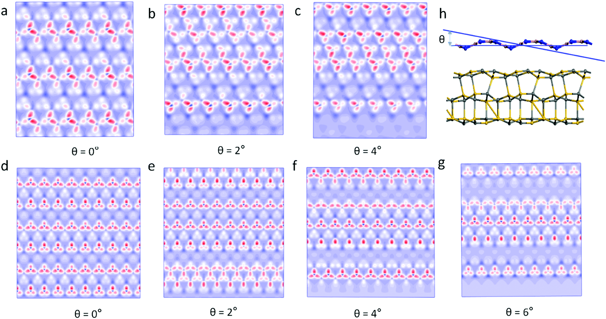
Previous studies have found that the moiré pattern is obtained by rotating the angle of two atomic layers of 2D materials.18 However, we found that the 2D material with a single layer of the wave shape structure can obtain moiré patterns at different incident angles. Fig. 3 shows the moiré pattern of BN/SiC-1 heterostructures with different incident angles of the BN layer. Therefore, the optical effect of the double-layer material geometry structure can be realized by the single layer shape wave geometry material. Furthermore, the wave shape structure of the h-BN surface is obtained by treating with H-plasma. In the experiment, the h-BN flakes appear as bubbles on the h-BN surface after H-plasma treatment.30 Also, a large strain will be generated on the h-BN surface by gas treatment. Our results show that lattice strain >5% will cause a moiré pattern on the BN/SiC heterojunctions. The results obtained in the experiment are consistent with our calculations.
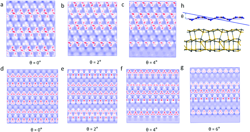 |
| | Fig. 3 Moiré pattern of BN/SiC-1 with incident angles of (a) θ = 0°, (b) θ = 2°, (c) θ = 4°, and BN/SiC-2 with incident angles of (d) 0 Å, (e) θ = 2°, (f) θ = 4°, (g) θ = 6°; and (h) heterostructures with incident angle θ on the BN layer. | |
3.2 Band structure, work function, and density of states (DOS)
We determine the band structures of the atomic monolayers of BN and SiC, whose band gaps are listed in Table 3. It can be seen from Fig. 4 that the band gaps of the atomic layers of BN and SiC are 4.661 and 2.108 eV, respectively. The band gaps of the BN/SiC van der Waals heterojunction structures 1 and 2 are 0.851 and 1.373 eV, respectively. The band gap of BN is reduced to approximately 0.7∼1.4 eV. We find that the BN strain of structure 1 (7.37%) is higher than that of structure 2 (5.93%), whereas the band gap of structure 1 (0.851 eV) is lesser than that of structure 2 (1.373 eV). The results indicate that the strain of BN/SiC increases, as the band gap decreases.
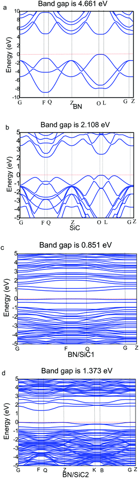 |
| | Fig. 4 Band structure of (a) BN, (b) SiC, (c) BN/SiC-1, and (d) BN/SiC-2. | |
We calculate the work function of the BN/SiC heterostructures, as presented in Table 3. The work function is the initial energy of the Fermi level and can be defined as the minimum energy required by the electrons to escape into a vacuum from the inside of the metal. In semiconductors, the energy at the bottom of the conduction band and valence band is typically lower than the minimum energy required for the electrons to escape from the metal. The work functions of BN/SiC structures 1 and 2 are 4.512 and 4.912 eV, respectively. A lower work function implies that electrons can easily escape the surface of the BN/SiC heterostructure. It can be seen from Table 3 that the work function of BN/SiC structure 1 is smaller than that of structure 2, which implies that the electrons of BN/SiC structure 1 can easily escape the surface than those of structure 2.
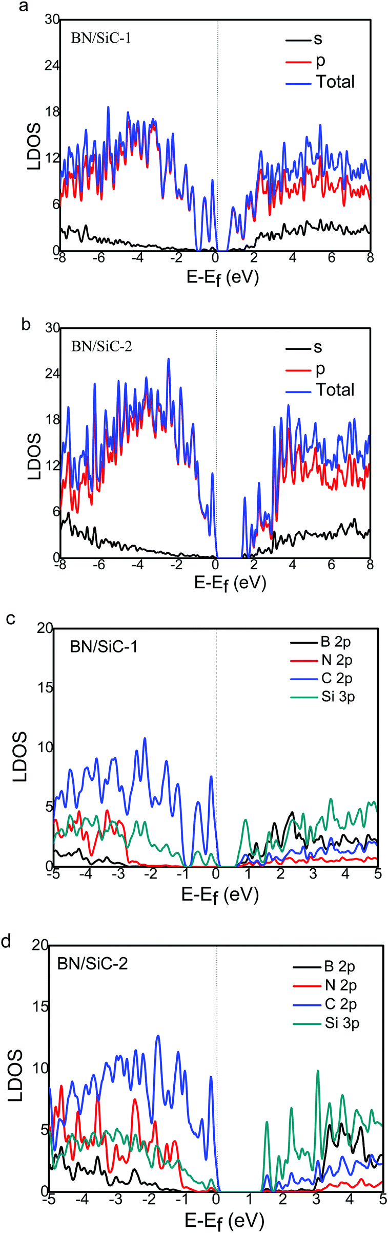
We calculate the local density of states (LDOS) of the BN/SiC heterojunction, as depicted in Fig. 6. From Fig. 6a and b, we can see that the electronic distributions of the conduction band minimum (CBM) of the BN/SiC structures 1 and 2 are 0.851 and 1.373 eV, respectively. The electrons in the valence band maximum (VBM) are mainly distributed in Fermi surface EF. The LDOS is mainly contributed by the p orbital in the range from −2 to 2 eV; therefore, we compared the contribution of C 2p, Si 2p, B 2p, and N 3p atoms to the band structure, as depicted in Fig. 6c and d. We found that the main orbital contribution to the CBM and VBM of the BN/SiC structures 1 and 2 originates from the Si 3p and C 2p orbitals. The results indicate that the SiC substrate has a significant influence on the BN band structure in the BN/SiC van der Waals heterojunction.
 |
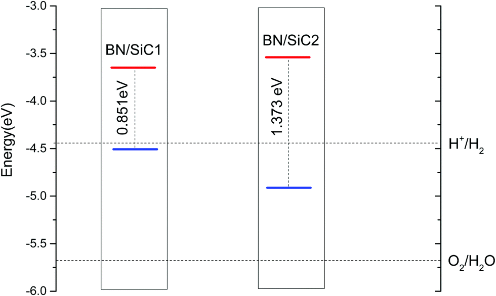
| | Fig. 5 The band edge alignment of BN/SiC-1 and BN/SiC-2 heterostructures. | |
The band arrangement of the heterojunction relative to the potential of the hydrogen evolution reaction/oxygen evolution reaction (HER/OER) has an important influence on the photocatalytic decomposition of water.31 The energies of the hydrogen (H+/H2) and oxygen evolution (O2/H2O) are −4.44 and −5.67 eV, respectively.32Fig. 5 compares the band edge positions of the BN/SiC structures 1 and 2 of hydrogen evolution (H+/H2) and oxygen evolution (O2/H2O). As seen in Fig. 6, the energies of the BN/SiC-2 structure of the CBM and VBM relative to the vacuum level are −3.539 and −4.912 eV, respectively. Our results reveal that the BN/SiC-2 heterostructure could be a promising material for hydrogen evolution and optoelectronic devices.
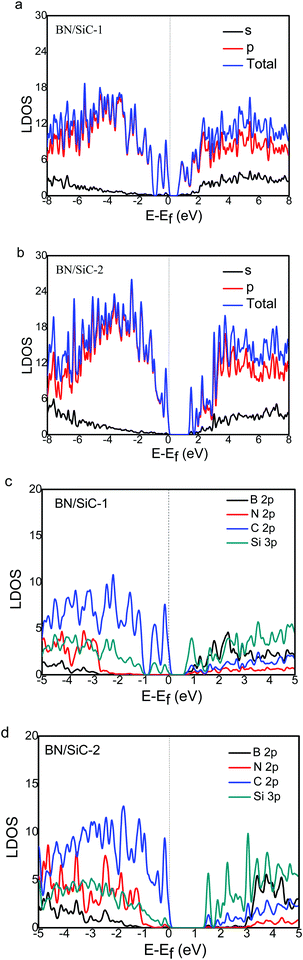 |
| | Fig. 6 The s- and p-orbital DOS of (a) BN/SiC-1 and (b) BN/SiC-2 heterostructures. The B, N, C and Si atoms DOS of (c) BN/SiC-1 and (d) BN/SiC-2 heterostructures. | |
3.3 Chemical bonding states and deformation charge density
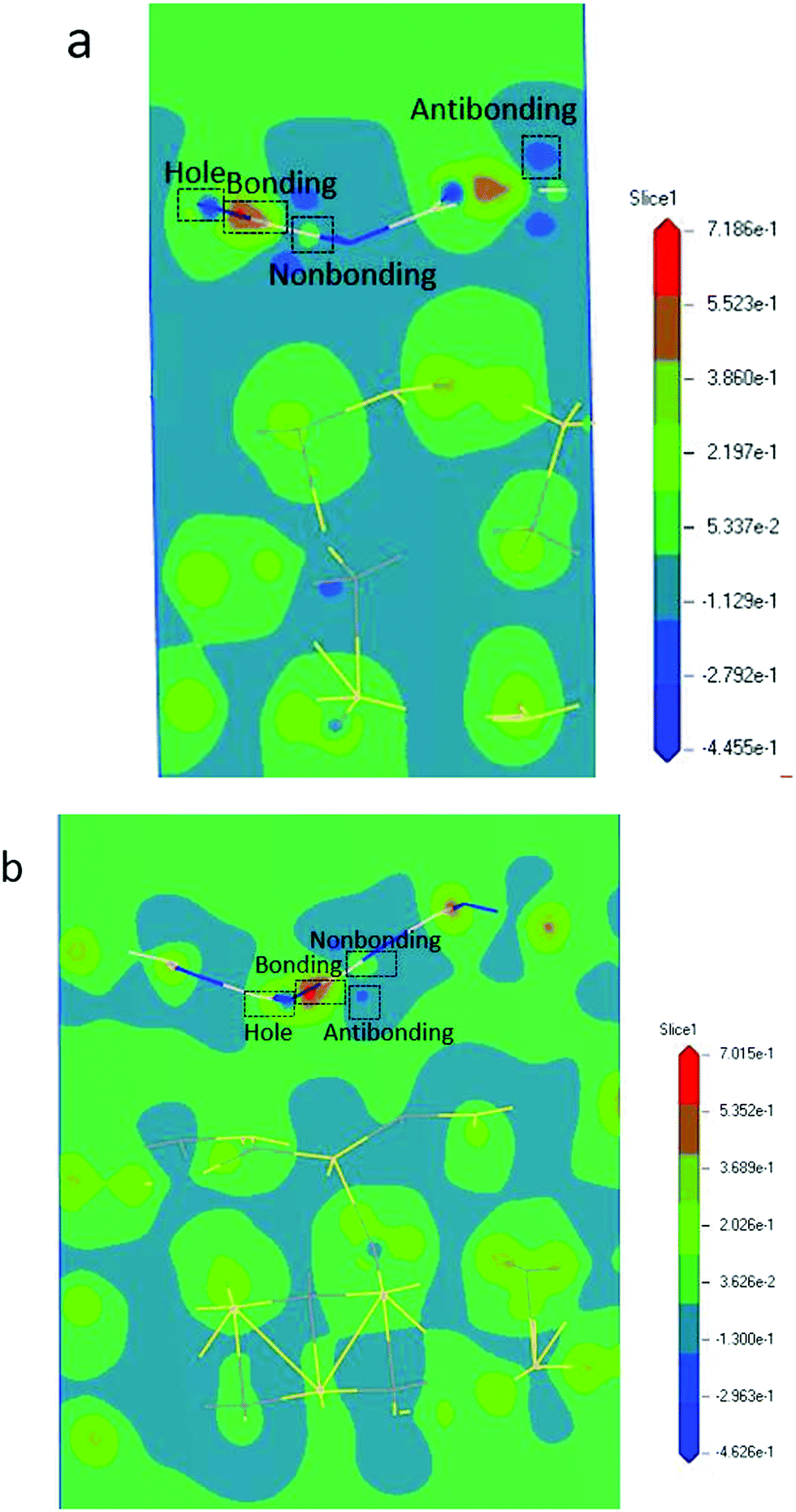
From the BOLS-BC model, we derived the following formula for calculating the atomic energy density ED (eV nm−3) of a 2D heterojunction: ED(z) = (1 − ![[small epsilon, Greek, macron]](https://www.rsc.org/images/entities/i_char_e0c6.gif) )−(m+3). The parameter m is the indicator of the nature of the bond. The lattice strain of each atom determines the distribution of energy density; a high energy density causes a high lattice strain ε. We believe that the formation of BN/SiC van der Waals heterostructures is primarily due to bond, electron, and charge contributions. Deformation charge density (e Å−3) is a tool used to study the electron transfer between atoms. In Fig. 7, we depict the electronic states of four chemical bonding states, namely, the antibonding, nonbonding, and bonding states and electron holes.33 The blue area represents the loss of electrons, and the red area represents the acquisition of electrons.
)−(m+3). The parameter m is the indicator of the nature of the bond. The lattice strain of each atom determines the distribution of energy density; a high energy density causes a high lattice strain ε. We believe that the formation of BN/SiC van der Waals heterostructures is primarily due to bond, electron, and charge contributions. Deformation charge density (e Å−3) is a tool used to study the electron transfer between atoms. In Fig. 7, we depict the electronic states of four chemical bonding states, namely, the antibonding, nonbonding, and bonding states and electron holes.33 The blue area represents the loss of electrons, and the red area represents the acquisition of electrons.
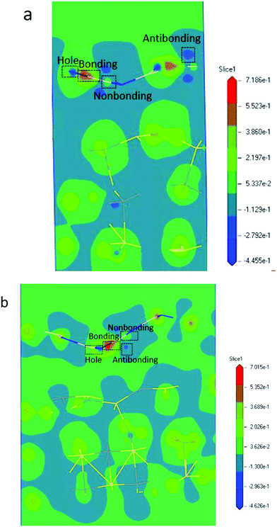 |
| | Fig. 7 Deformation charge density of (a) BN/SiC-1 and (b) BN/SiC-2 heterostructures resolved bonding states and electron features: nonbonding, antibonding, and bonding states, as well as electron holes. | |
Antibonding states indicate the electron density and bond energy decrease in the region. Nonbonding states indicate that the electron density increases in the region, but the surrounding electron density does not overlap with the electron density of the other atoms. Bonding states indicate that the electron density increases in the region, but the electron density overlaps with the other atomic electron densities, indicating that the atom is in the bonding state. Electron holes indicate that the electron density decreases in the region, with a high concentration around the nucleus.
Furthermore, by defining the electronic states of the chemical bonding, we establish the expressions for the deformation charge density and potential function of the chemical bond states. The chemical bond potential function can be obtained by calculating the differential charge density. We used eqn (2) to calculate the potential functions of the antibonding, nonbonding, and bonding states. Comparing the potential functions, we obtain Vbondingcry(r) > Vnonbondingcry(r) > VAntibondingcry(r). We also calculate the potential function of the atomic bonding states, as presented in Table 5. These results improve the theoretical reference for analyzing the quantitative bond properties of materials.
Table 5 Chemical bonding states, deformation charge density Δρi(r), and potential functions Vcry(ri) of the van der Waals heterojunctions using the calculated BC (ε0 = 8.85 × 10⁻¹² C2 N−1 m−2, e = 1.60 × 10⁻¹⁹ C)
|
|
BN/SiC-1 (r = d/2 = 1.445/2 Å) |
BN/SiC-2 (r = d/2 = 1.425/2 Å) |
| Δρhole(ri) (e Å−3) |
−4.455 × 10⁻¹ |
−4.626 × 10⁻¹ |
| Δρbonding-electron(ri) (e Å−3) |
7.186 × 10⁻¹ |
7.015 × 10⁻¹ |
| Δρnonbonding-electron(ri) (e Å−3) |
2.197 × 10⁻¹ |
2.026 × 10⁻¹ |
| Δρantibonding-electron(ri) (e Å−3) |
−2.792 × 10⁻¹ |
−2.963 × 10⁻¹ |
|
V
nonbondingcry(ri) (eV) |
−1.460 |
−1.248 |
|
V
bondingcry(ri) (eV) |
−4.775 |
−4.322 |
|
V
Antibondingcry(ri) (eV) |
1.855 |
1.825 |
4. Conclusions
In this study, we investigated the geometric, energetic, electronic, and photocatalytic properties of BN/SiC van der Waals heterostructures. A lattice strain >5% results from the wave-shaped geometry structure of the BN/SiC heterojunctions. The wave shape can cause a moiré pattern with different incident angles. The BN/SiC van der Waals heterojunctions 1 and 2 will form moiré patterns at different incident angles, which can be applied in photoelectric detection technology. The BN/SiC van der Waals heterostructures 1 and 2 exhibit a band gap of 0.851 and 1.373 eV, respectively. The band arrangement shows that the BN/SiC van der Waals heterojunction is a potential photoelectric material candidate. The DFT calculation and BOLS-BC model reveal the characteristics of the charge density and chemical bonds on the heterojunction's material surface. These results improve the theoretical reference for the analysis of the quantitative bond and charge properties of 2D heterojunction materials.
Conflicts of interest
There are no conflicts to declare.
Acknowledgements
Financial support was provided by the National Natural Science Foundation of China (Grant No. 11947021) and the Research Program of Chongqing Municipal Education Commission (Grant No. KJQN201901421).
References
- K. S. Novoselov, A. K. Geim, S. V. Morozov, D. Jiang, Y. Zhang, S. V. Dubonos, I. V. Grigorieva and A. A. Firsov, Science, 2004, 306, 666–669 CrossRef CAS PubMed.
- L. Li, Y. Yu, G. J. Ye, Q. Ge, X. Ou, H. Wu, D. Feng, X. H. Chen and Y. Zhang, Nat. Nanotechnol., 2014, 9, 372 CrossRef CAS PubMed.
- A. Splendiani, L. Sun, Y. Zhang, T. Li, J. Kim, C.-Y. Chim, G. Galli and F. Wang, Nano Lett., 2010, 10, 1271–1275 CrossRef CAS PubMed.
- M. Pumera and Z. Sofer, Adv. Mater., 2017, 29, 1605299 CrossRef PubMed.
- K. S. Novoselov, D. Jiang, F. Schedin, T. J. Booth, V. V. Khotkevich, S. V. Morozov and A. K. Geim, Proc. Natl. Acad. Sci. U. S. A., 2005, 102, 10451–10453 CrossRef CAS PubMed.
- M. Bo, J. Li, C. Yao, Z. Huang, L. Li, C. Q. Sun and C. Peng, RSC Adv., 2019, 9, 9342–9347 RSC.
- T. Hu and J. Hong, ACS Appl. Mater. Interfaces, 2015, 7, 23489–23495 CrossRef CAS PubMed.
- J. Qi, X. Qian, L. Qi, J. Feng, D. Shi and J. Li, Nano Lett., 2012, 12, 1224–1228 CrossRef CAS PubMed.
- Y. R. Tang, Y. Zhang and J. X. Cao, J. Appl. Phys., 2016, 119, 195303 CrossRef.
- J. He, N. Jiao, C. Zhang, H. Xiao, X. Chen and L. Sun, J. Phys. Chem. C, 2014, 118, 8899–8906 CrossRef CAS.
- J. Wang, H. Shu, P. Liang, N. Wang, D. Cao and X. Chen, J. Phys. Chem. C, 2019, 123, 3861–3867 CrossRef CAS.
- D. S. Koda, F. Bechstedt, M. Marques and L. K. Teles, J. Phys. Chem. C, 2017, 121, 3862–3869 CrossRef CAS.
- K. Tang, W. Qi, Y. Li and T. Wang, J. Phys. Chem. C, 2018, 122, 7027–7032 CrossRef CAS.
- B. Sachs, T. O. Wehling, M. I. Katsnelson and A. I. Lichtenstein, Phys. Rev. B: Condens. Matter Mater. Phys., 2011, 84, 195414 CrossRef.
- G. Chen, A. L. Sharpe, P. Gallagher, I. T. Rosen, E. J. Fox, L. Jiang, B. Lyu, H. Li, K. Watanabe, T. Taniguchi, J. Jung, Z. Shi, D. Goldhaber-Gordon, Y. Zhang and F. Wang, Nature, 2019, 572, 215–219 CrossRef CAS PubMed.
- M. M. van Wijk, A. Schuring, M. I. Katsnelson and A. Fasolino, Phys. Rev. Lett., 2014, 113, 135504 CrossRef CAS PubMed.
- C. Zhang, C.-P. Chuu, X. Ren, M.-Y. Li, L.-J. Li, C. Jin, M.-Y. Chou and C.-K. Shih, Sci. Adv., 2017, 3, e1601459 CrossRef PubMed.
- M. R. Rosenberger, H.-J. Chuang, M. Phillips, V. P. Oleshko, K. M. McCreary, S. V. Sivaram, C. S. Hellberg and B. T. Jonker, ACS Nano, 2020, 14(4), 4550–4558 CrossRef CAS PubMed.
- Y. Cao, V. Fatemi, S. Fang, K. Watanabe, T. Taniguchi, E. Kaxiras and P. Jarillo-Herrero, Nature, 2018, 556, 43 CrossRef CAS PubMed.
- J. Kang, J. Li, S.-S. Li, J.-B. Xia and L.-W. Wang, Nano Lett., 2013, 13, 5485–5490 CrossRef CAS PubMed.
- S. K. Hämäläinen, M. P. Boneschanscher, P. H. Jacobse, I. Swart, K. Pussi, W. Moritz, J. Lahtinen, P. Liljeroth and J. Sainio, Phys. Rev. B: Condens. Matter Mater. Phys., 2013, 88, 201406 CrossRef.
- M. Sicot, S. Bouvron, O. Zander, U. Rüdiger, Y. S. Dedkov and M. Fonin, Appl. Phys. Lett., 2010, 96, 093115 CrossRef.
- M. Yankowitz, J. Jung, E. Laksono, N. Leconte, B. L. Chittari, K. Watanabe, T. Taniguchi, S. Adam, D. Graf and C. R. Dean, Nature, 2018, 557, 404–408 CrossRef CAS PubMed.
- J. R. Wallbank, M. Mucha-Kruczyński, X. Chen and V. I. Fal'ko, Ann. Phys., 2015, 527, 359–376 CrossRef CAS.
- J. Heyd, G. E. Scuseria and M. Ernzerhof, J. Chem. Phys., 2003, 118, 8207–8215 CrossRef CAS.
- M. Bo, Y. Wang, Y. Huang, Y. Liu, C. Li and C. Q. Sun, Appl. Surf. Sci., 2015, 325, 33–38 CrossRef CAS.
-
C. Q. Sun, Relaxation of the Chemical Bond, Heidelberg, New York, Dordrecht, London, Singapore, 2014 Search PubMed.
- M. Bo, Y. Guo, Y. Wang, Y. Liu, C. Peng, C. Q. Sun and Y. Huang, Phys. Chem. Chem. Phys., 2016, 18, 13280–13286 RSC.
- J. Liao, B. Sa, J. Zhou, R. Ahuja and Z. Sun, J. Phys. Chem. C, 2014, 118, 17594–17599 CrossRef CAS.
- L. He, H. Wang, L. Chen, X. Wang, H. Xie, C. Jiang, C. Li, K. Elibol, J. Meyer, K. Watanabe, T. Taniguchi, Z. Wu, W. Wang, Z. Ni, X. Miao, C. Zhang, D. Zhang, H. Wang and X. Xie, Nat. Commun., 2019, 10, 2815 CrossRef PubMed.
- S. Tang, J. Yu and L. Liu, Phys. Chem. Chem. Phys., 2013, 15, 5067–5077 RSC.
- G. Wang, L. Zhang, Y. Li, W. Zhao, A. Kuang, Y. Li, L. Xia, Y. Li and S. Xiao, J. Phys. D: Appl. Phys., 2019, 53, 015104 CrossRef.
- M. Bo, L. Li, Y. Guo, C. Yao, C. Peng and C. Q. Sun, Appl. Surf. Sci., 2018, 427, 1182–1188 CrossRef CAS.
Footnote |
| † Electronic supplementary information (ESI) available. See DOI: 10.1039/d0ma00258e |
|
| This journal is © The Royal Society of Chemistry 2020 |
Click here to see how this site uses Cookies. View our privacy policy here. 
 Open Access Article
 This Open Access Article is licensed under a
  *,
Hanze
Li
,
Anlin
Deng
,
Lei
Li
,
Chuang
Yao
*,
Hanze
Li
,
Anlin
Deng
,
Lei
Li
,
Chuang
Yao