
 Open Access Article
 This Open Access Article is licensed under a Creative Commons Attribution-Non Commercial 3.0 Unported Licence
A facile and robust approach to prepare fluorinated polymer dielectrics for probing the intrinsic transport behavior of organic semiconductors†
Jenner H. L.
Ngai
 ,
Cyril Chak Ming
Chan
,
Carr Hoi Yi
Ho
,
Johnny Ka Wai
Ho
,
Sin Hang
Cheung
,
Hang
Yin
and
Shu Kong
So
*
,
Cyril Chak Ming
Chan
,
Carr Hoi Yi
Ho
,
Johnny Ka Wai
Ho
,
Sin Hang
Cheung
,
Hang
Yin
and
Shu Kong
So
*
Department of Physics and Institute of Advanced Materials, Hong Kong Baptist University, Kowloon Tong, Hong Kong. E-mail: skso@hkbu.edu.hk
First published on 18th June 2020
Abstract
Insulating polymers are often used as gate dielectric materials in all-solution processable organic thin-film transistors (OTFTs). Nonetheless, most of the polymers have poor resistance to common halogenated solvents and thus are not feasible for bottom-gate OTFT structures. In this contribution, we show that high molecular weight poly(2,3,4,5,6-pentafluorostyrene) (PPFS) is a gate dielectric material that can be free from this limitation. We prepare PPFS with a facile and efficient approach by using methyl isobutyl ketone (MIK) solvent in a basic wet-lab without the need of complex chemical equipment. Furthermore, the non-polar and hydrophobic nature of the PPFS surface allows us to probe the intrinsic transport behaviors of these acceptors. The MIK solvent-assisted polymerization method provides an alternative for low-cost effective gate polymer dielectric preparation. Such a novel but simple synthesis paradigm not only opens up a broad employment of solution-processable polymeric dielectrics for bottom-gate OTFTs, but also enables the full device potential with high-mobility semiconductors.
Organic thin-film transistors (OTFTs) have gained enormous research interests in a number of applications such as flexible displays, radio frequency identification, and chemical and biological sensors.1–12 Of all of the high mobility devices reported, dielectric layers played an important role in governing the charge transport process in OTFTs. To achieve high carrier mobility in OTFTs, high-κ and small-d are two well-recognized factors that a dielectric material should possess in OTFT devices.13–15 For the bottom gate TFT structure, there are not so many polymer dielectrics that are compatible for all-solution processing. Most organic semiconductors use halogenated solvents (e.g. chlorobenzene and chloroform) as common solvents, but most of the polymer gate dielectric materials have poor solubility resistance to these solvents.
Cross-linking and post-etching are two normal strategies to address the problem of high solubility of polymers in halogenated solvents.16 For the cross-linking method, there could be incomplete consumption of the crosslinking agents which may stay within the polymer and induce electron or hole traps during charge transport in transistor operation.17 Moreover, many of these crosslinking agents are silane-based chemicals in which the unreacted silane crosslinkers may be detrimental to TFT operations.18,19 Previously, high molecular weight vinyl polymers were usually synthesized by degassed solvents under inert atmospheres. Chan et al. prepared a PPFS polymer with a weight average molecular weight of 98 kDa under degassed solventless conditions under an argon atmosphere.20 The polymerization ended in 20 hours and the polymer obtained was a glass-like solid. The polymerization was believed to be quenched by polymer chain entanglement which caused a lower polymerization reactivity by increasing the solution viscosity during polymer growth.21 The final polymer was soluble in chloroform. Huang et al. also reported the synthesis of PPFS back in the 1960s, but once again the polymer was synthesized using a complicated polymerization set-up and techniques such as high vacuum systems, extremely low temperature preparatory conditions, and free-dry cycle techniques.22
Here, we identify poly(2,3,4,5,6-pentafluorostyrene) (PPFS) as a candidate for solution processable gate dielectrics for bottom-gate TFTs. We chose methyl isobutyl ketone (MIK) as solvent and synthesize high molecular weight PPFS by radical polymerization with a simple set-up (Scheme 1).
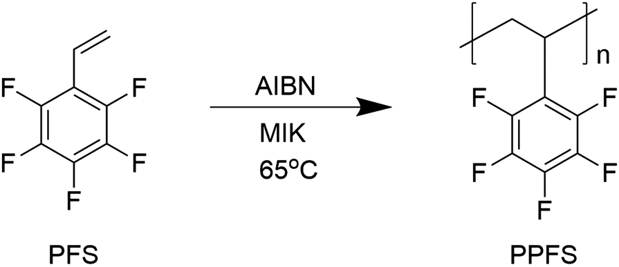 | ||
| Scheme 1 General synthetic procedure of poly(2,3,4,5,6-pentafluorostyrene) (PPFS). | ||
With the MIK solvent-assisted radical polymerization approach, we can produce high molecular weight PPFS polymers with a highest weight average molecular weight of 213 kDa. It was also reported that PPFS homopolymer with a molecular weight of 13.8 kDa had a better solubility in MIK than in chloroform.23 Kim et al. extensively studied PPFS as a dielectric in OTFTs.24 Interestingly, our reported PPFS polymer with such a high molecular weight becomes insoluble in chloroform or halogenated-solvents and is only soluble in ketone solvents such as MIK. In such a case, our PPFS polymer was found to be an ideal candidate for dielectric materials in all-solution processed OTFTs having the bottom-gate-top-contact (BGTC) device architecture without the use of a crosslinking agent to create a bottom insoluble dielectric layer. It can avoid any dissolution during the upper layer deposition, which can lead to unwanted interfacial mixing and increased interface roughness. MIK is also a solvent with low mammalian and aquatic toxicity, together with negligible environmental hazards.25 This fluorinated polymer can also be synthesized easily without the use of a high vacuum system and inert atmosphere which is typically required for high molecular weight polymer synthesis. The production of PPFS is robust and the purification method is also simple. The entire production process can be carried out either in a glovebox or in a closed container under ambient conditions in a basic wet-lab. Complicated chemical instruments such as a rotary evaporator or quick-fit apparatus were not required for the synthesis of the polymer. The dielectric constant of the PPFS polymer was found to be as high as 2.8, and it can form a pinhole-free smooth thin film as thin as 35 nm. The unique halogenated solvent resistance property of the polymer may also be applied in inkjet printing and can possibly be employed in large scale inexpensive printable electronics, and substitute other high-cost fluoropolymer dielectric candidates, such as CYTOPTM. The dielectric constant, solvent resistance and wetting properties of some common commercial polymer dielectric materials and fluorinated dielectric materials are summarized in Table 1. In the ESI,† we show the chemical structure of PVDF and the frequency dependent dielectric constant of PPFS and PVDF for comparison (Fig. S1 and S2, ESI†).
| Polymer | Dielectric constant | Resistance to halogenated solvents | Wetting properties | Ref. |
|---|---|---|---|---|
| a Poor solvent resistance which made spin-coating of another layer of material impossible due to the high solubility of the material in organic solvents. | ||||
| PPFS | 2.8 (3.7) | Good | Good | This work |
| CYTOPTM | 2.0 | Good | Moderate | 46 |
| PVDF | 8.7 | Good | Moderate | This work |
| PS | 2.6 | Poor | N/Aa | 47 |
| PMMA | 3.5 | Poor | N/Aa | 47 |
Synthesis and properties of PPFS
Synthesis of poly(2,3,4,5,6-pentafluorostyrene) (PPFS)
The MIK solvent-assisted radical polymerization approach was performed under two different environments, namely the nitrogen-filled conditions and ambient conditions. The details are as follows.Nitrogen-filled conditions
2,3,4,5,6-Pentafluorostyrene (5.00 g, 25.8 mmol), 2,2′-azobis(2-methylpropionitrile) (4.23 mg, 0.0258 mmol) and 3.00 mL methyl isobutyl ketone were added into a 10 mL Schlenk tube inside a nitrogen-filled glovebox (O2 and H2O <1 ppm). A magnetic stirrer was then put into the tube and sealed tightly with a screw cap. The Schlenk tube was then taken out of the glovebox and the solution mixture was submerged into a silicone oil bath at 65 °C under vigorous stirring for 120 minutes. After cooling down the mixture, the viscous solution was then precipitated into 400 mL isopropanol. A white precipitate was then filtered and collected. The precipitate was re-dissolved into a minimum amount of methyl isobutyl ketone and re-precipitated into 400 mL methanol. The precipitated polymers were submerged in methanol for 30 minutes and then filtered. The white powder was then washed successively with methanol and dried in vacuo to give PPFS as a white powder (4.35 g, 87% yield).Ambient conditions
2,3,4,5,6-Pentafluorostyrene (5.00 g, 25.8 mmol), 2,2′-azobis(2-methylpropionitrile) (4.23 mg, 0.0258 mmol) and 3.00 mL methyl isobutyl ketone were added to a 20 mL glass vial in air. A magnetic stirrer was then put into the vial and sealed tightly with a screw cap. The glass vial was then placed on a hotplate at 65 °C under vigorous stirring for 18 hours. After cooling down the mixture, the solution was worked up using the same procedure as described by the glovebox approach to give PPFS as a white powder (4.01 g, 80% yield).Physical properties of poly(2,3,4,5,6-pentafluorostyrene) (PPFS)
Size Exclusion Chromatography (SEC) was used to estimate the molecular weight of the synthesized polymers according to their hydrodynamic volume. The SEC chromatograms and molecular weight distribution of PPFS synthesized by a MIK solvent-assisted radical polymerization approach in both the glovebox and ambient environments are shown in Fig. 1. | ||
| Fig. 1 (a) SEC chromatograms and (b) molecular weight distributions extracted from chromatography data of poly(2,3,4,5,6-pentafluorostyrene) (PPFS) via different synthetic conditions. | ||
The weight average molecular weight (Mw) of the polymers was found to be 213 and 107 kDa respectively, and similar polydispersities (Đ) of 2.2 were observed for both polymers. The lower molecular weight obtained from the ambient environment could possibly be due to the retardation of the radical polymerization by oxygen or moisture under ambient conditions. However, the molecular weight was still high when using the MIK ketone solvent as the reaction medium. Thermal analyses for glass transition temperature estimation were also examined by differential scanning calorimetry (DSC). The DSC spectra can be found in Fig. S3 and S4 (ESI†). The glass transition temperatures (Tg) of PPFS synthesized by glovebox and ambient approaches were both 109 °C, which indicates a high degree of polymerization. The physical information of PPFS polymers synthesized via different approaches is provided in Table 2.
n-OTFT performances employing PPFS as a dielectric material
OTFTs with PPFS as the gate dielectric layer were tested with different common n-type materials containing PC71BM, N2200, ITIC and ITIC-Th.26–28 The molecular weight of N2200 is 200 kDa with a polydispersity index of 2.5 in this work. The chemical structures of these materials are shown in Fig. 2. PPFS films with a thickness of about 30 nm were spun-cast on p++Si/SiO2 substrates from methyl isobutyl ketone (MIK). Atomic force microscopy (AFM) and optical microscopy (OM) were performed to investigate the PPFS-treated SiO2 surface. The 2 μm × 2 μm AFM image (Fig. 3a) showed smooth and featureless textures with a root-mean-square surface roughness of 0.36 nm, and the 50 μm × 50 μm OM image presented a pin-hole free surface, meaning that PPFS is helpful to form a high-quality semiconductor/dielectric interface (Fig. 3b). The water contact angle on PPFS is 90° (Fig. 3c). The hydrophobic surface originates from the fluorine atom in PPFS, and can effectively repel water and oxygen to prevent interfacial trap formation in the boundary of semiconductors and gate-dielectrics. A bottom-gate-top-contact OTFT with device structure p++Si/SiO2/PPFS/n-type semiconductor/PDIN/Al was adopted (Fig. 3d). AFM images of the organic solvent treated PPFS thin film were also taken to assess its chemical resistance to common solvents. The AFM images showed a similar morphology and roughness to the untreated film (Fig. S5, ESI†). | ||
| Fig. 2 Chemical structures of the four n-type organic semiconductors studied in this work. | ||
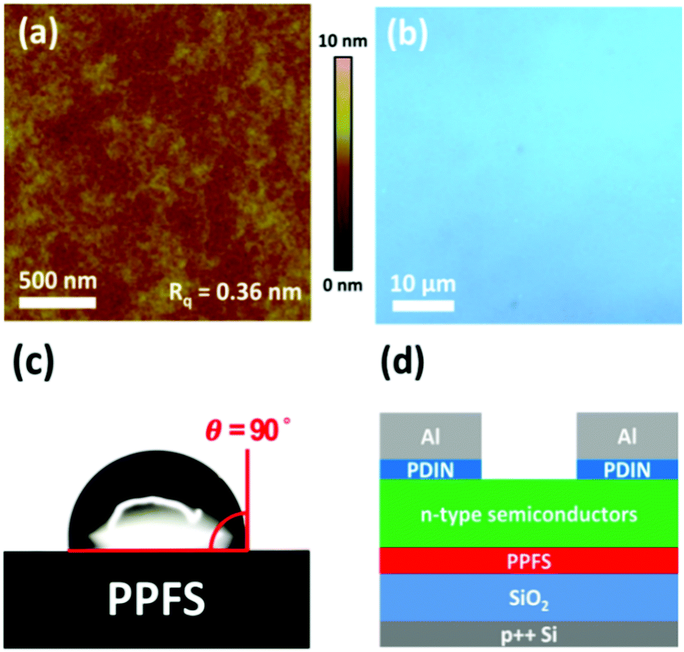 | ||
| Fig. 3 (a) 2 μm × 2 μm atomic force microscopy and (b) 50 μm × 50 μm optical microscopy images of the PPFS film surface. (c) Water contact angle on the PPFS-coated SiO2 surface. (d) Schematic diagram of a bottom-gate-top-contact (BGTC) OTFT. | ||
After the coating of the n-type semiconductor active layer, a perylene diimide derivative with an amino terminal substituent namely 2,9-bis(3-(dimethylamino)propyl)anthra[2,1,9-def:6,5,10-d′e′f′]diisoquinoline-1,3,8,10(2H,9H)-tetraone (PDIN) was employed as an electron injection layer. The chemical structure of PDIN is shown in Fig. S1 (ESI†).
Fig. 4(a)–(d) show the TFT output characteristics of the n-type transistors. All transistors exhibited well field-effect transistor behaviors in both the linear and saturation regimes. The PC71BM OTFT showed the best electron transport characteristic, with μsat = 5.4 × 10⁻³ cm2 V−1 s−1, a small threshold voltage of 7.7 V, and four orders of magnitude on/off current ratio. In the evaluation of mobilities, the effective dielectric constant of 3.7 from Table 1 was used. Generally, the TFTs with PDIN contacts showed no observable contact resistance and very good and clear saturation behavior. Their corresponding saturation mobilities (μsat), current on–off ratios and threshold voltages (VT) were evaluated using eqn (1) and can be found in Table 3. To assess the reliability of our TFT results, we compared our values with the highest reported mobilities from the literature.29–31 The results are also summarized in Table 3. The mobility values of PCBM, ITIC and ITIC-Th are similar. For N2200, the mobilities are almost 3 orders less. The difference of N2200 electron mobilities may have come from the different molecular weight of N2200 and TFT architecture employed (top-gate bottom-contact vs. bottom gate top contact). Our TFTs have reasonably low off-current (∼10–10 A). The intrinsic low carrier mobility of the active layer materials limits the on-current, hence the on–off ratio. Nevertheless, comparing the on–off ratios with reported literature values, our devices are still in an acceptable range (103–104 cm2 V−1 s−1).32–37
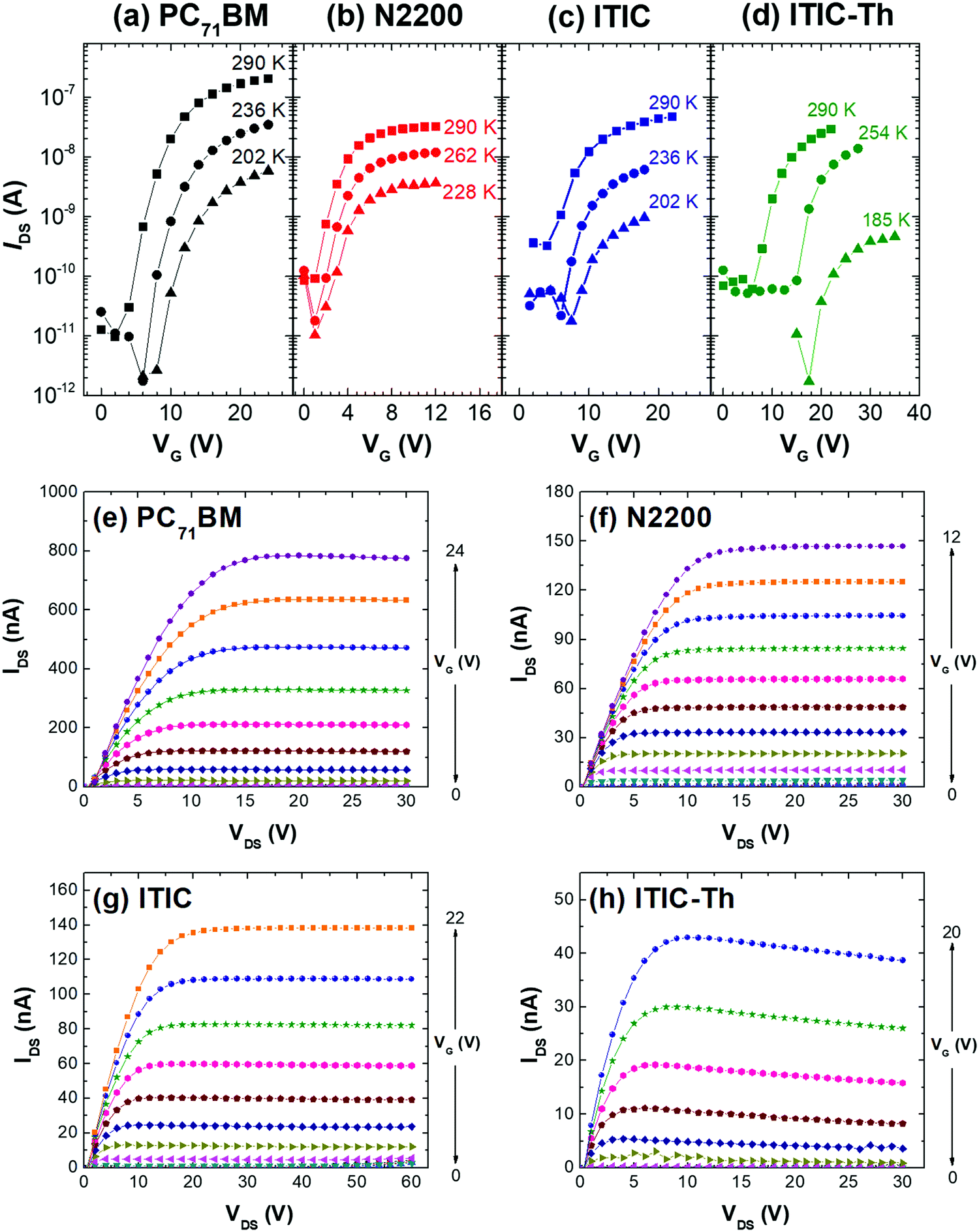 | ||
| Fig. 4 Transfer and output characteristics of OTFTs using (a and e) PC71BM; (b and f) N2200; (c and g) ITIC and (d and h) ITIC-Th as the active layers. | ||
| Active material | μ lin (cm2 V−1 s−1) | μ sat (cm2 V−1 s−1) | V T (V) | I on/off |
|---|---|---|---|---|
| PC71BM | 4.5 × 10⁻³ | 5.4 × 10⁻³ | 7.7 | 2.1 × 10⁴ |
| N2200 | 2.6 × 10⁻³ | 2.3 × 10⁻³ | 1.0 | 4.1 × 10² |
| ITIC | 7.6 × 10⁻⁴ | 8.7 × 10⁻⁴ | 4.9 | 6.9 × 10² |
| ITIC-Th | 9.8 × 10⁻⁴ | 5.3 × 10⁻⁴ | 8.8 | 2.9 × 10² |
For completeness, we also fabricated TFTs without the PDIN contact layers. The results are summarized in the ESI† (Fig. S6 and Table S1). All TFT mobilities are slightly reduced compared to those with PDIN contacts, demonstrating the beneficial roles of the PDIN layers. In addition, they show insignificant hysteresis (Fig. 5).
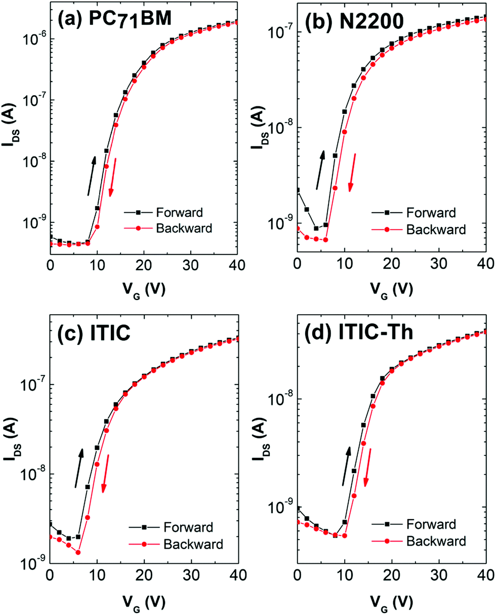 | ||
| Fig. 5 Hysteresis study of (a) PC71BM, (b) N2200, (c) ITIC and (d) ITIC-Th with transfer characteristic at VDS = 60 V and VG sweep rate of 1 V s−1. | ||
We also attempted to fabricate a PC71BM n-type OTFT employing two other fluorinated polymers, polyvinylidene difluoride (PVDF) (Fig. S1, ESI†) and CYTOPTM as gate dielectrics. When using PVDF, it showed lower saturation mobility (1.2 × 10⁻³ cm2 V−1 s−1) and much higher threshold voltage (27 V) (Fig. S7, ESI†). PC71BM showed poor wettability on CYTOPTM and cannot be used further for OTFT fabrication. The water contact angle on CYTOPTM was found to be as large as 107°, suggesting that CYTOPTM has a lower surface free energy, and should be incompatible for bottom gate structures in all-solution process OTFTs (Fig. S8, ESI†).
In organic electronics, PC71BM, N2200, ITIC, and ITIC-Th are probably the most widely used acceptors in organic photovoltaic cells.27,29 Their n-type transport behaviors are of clear importance for understanding their electronic properties. A PPFS gate dielectric layer can serve as an ideal substrate to assess electron transport in these acceptors. PPFS has two notable advantages. First it is non-polar, so the transport of electrons in the active layer will not be affected by the local dipoles from the gate dielectric/active layer interface. Second, the hydrophobic nature of PPFS excludes moisture which can severely hinder electron transport. For the four electron acceptors under investigation, their lowest unoccupied molecular orbitals (LUMOs) can be taken to have a Gaussian distribution with an energy spread of σ, which is also known as the energetic disorder according to the well-known Gaussian Disorder Model (GDM).38 In this model, charges hop in an energetic manifold with a Gaussian density of states. The width of the manifold is σ. Under such a condition, the charge carrier mobility is temperature (T) and electric field (F) dependent and the mobility can be expressed as:38–41
 | (1) |
Temperature dependent mobility measurements were carried out for all 4 electron acceptors, and their low field (linear) electron mobilities were extracted. From a plot of μ0vs. 1/T2, the data can be seen to follow the GDM very well in all cases as shown in Fig. 6. From the linear fittings (solid straight lines in Fig. 6), both transport parameters, μ∞ and σ, can be extracted for all four electron acceptors. The results are summarized in Table 4. It can be seen that all acceptors possess low and similar energetic disorders σ in the range of 66–71 meV, which are favorable for electron transport. The μ∞ values for PC71BM and N2200 acceptors, however, are about four times larger than those of ITIC and ITIC-Th. As μ∞ is related to the intermolecular stacking,43,44 the lower μ∞ values for the ITIC-based acceptors suggest that these non-fullerene small molecular acceptors must be further improved in their morphology in order to reach higher mobilities in OPV applications.
 | ||
| Fig. 6 Zero field mobilities vs. 1/T2 for the four electron acceptors. The lines are the linear fits to the data using eqn (1). | ||
| Active material | μ ∞ (cm2 V−1 s−1) | σ (meV) |
|---|---|---|
| PC71BM | 9.4 × 10⁻² | 66 |
| N2200 | 8.4 × 10⁻² | 71 |
| ITIC | 1.9 × 10⁻² | 68 |
| ITIC-Th | 2.3 × 10⁻² | 67 |
Experimental section
Materials
2,2′-Azobis(2-methylpropionitrile), methyl isobutyl ketone, isopropanol and chloroform were purchased from Sigma Aldrich. ITIC and ITIC-Th were purchased from 1-material. PC71BM, N2200 and 2,3,4,5,6-pentafluorostyrene were purchased from nano-C, Polyera and Apollo Scientific respectively. 2,2′-Azobis(2-methylpropionitrile) was recrystallized by a method previously reported prior to use.45 Other chemicals were used as received.Size exclusion chromatography (SEC) and differential scanning calorimetry (DSC)
SEC was performed at room temperature using an HP 1050 series HPLC with an ultraviolet detector at 254 nm using tetrahydrofuran (THF) as the eluent (HPLC column: Jordi Gel GBR Mixed Bed, 300 mm × 7.8 mm). The SEC results were calibrated with polystyrene standards with molecular weights of 1350 (polydispersity index (Đ) = 1.03), 28![[thin space (1/6-em)]](https://www.rsc.org/images/entities/char_2009.gif) 000 (Đ = 1.01), 87000 (Đ = 1.02) and 410000 (Đ = 1.03). DSC was performed using a PerkinElmer Pyris Diamond differential scanning calorimeter.
000 (Đ = 1.01), 87000 (Đ = 1.02) and 410000 (Đ = 1.03). DSC was performed using a PerkinElmer Pyris Diamond differential scanning calorimeter.
TFT fabrication and measurement
The silicon wafers were first cleaned with deionized water, acetone, and isopropanol for 20 min each. After 13 min of UV-ozone treatment, PPFS dissolved in methyl isobutyl ketone (10 mg mL−1) was spun on the substrates at 2000 rpm for 40 s, giving a 25 nm thick film. The PPFS-treated wafers were then annealed at 120 °C for 2 hours to dry out the solvent. PC71BM, N2200ITIC and ITIC-Th were dissolved in chloroform with a concentration of 10 mg mL−1 and spin-coated on PPFS at 2000 rpm for 1 min. The thickness of the semiconductors was around 60 nm. After that PDIN which was dissolved in 2,2,2-trifluoroethanol with a concentration of 1 mg mL−1 was spun on the active layer at 7500 rpm for 1 min. On top of semiconductors, 100 nm aluminum was thermally evaporated under high vacuum, forming a channel length of 50 μm. Measurements were done in a cryostat (Oxford Instruments, Optistat DN-V) under vacuum below 10−4 Torr and dark conditions at various temperatures. A Keithley 236 source measurement unit together with a Xantrex XT 120-0.5 as the DC gate voltage supply was used.Atomic force microscopy
AFM images were scanned using Veeco diMultimodeV with a NanoscopeV controller. The E-scanner with an Appnano ACTA silicon probe scanned in a tapping mode provided information on surface height within a size of 2 μm × 2 μm.Conclusions
In summary, we have identified high molecular weight poly(2,3,4,5,6-pentafluorostyrene) (PPFS) as an excellent gate dielectric material for the fabrication of all-solution processable bottom-gate top-contact TFTs. A facile and robust method was designed to prepare PPFS so that the PPFS can be dissolved in methyl isobutyl ketone but remains insoluble in common solvents in good yield and high purity. The resulting PPFS layer is highly hydrophobic while at the same time permitted the adhesion of organic layers on top of this layer prepared by spin-coating. Four commonly used electron acceptors, including PC71BM, N2200, ITIC, and ITIC-Th, were tested on the PPFS layer. Their TFTs possess well-behaved output curves, and their electron mobilities were evaluated and lie in the range between 10−4 and 10−3 cm2 V−1 s−1. Furthermore, the non-polar and hydrophobic nature of the PPFS surface allows us to probe the intrinsic transport behaviors of these acceptors. The results suggest that the ITIC-based acceptors need to be improved in terms of their morphologies in order to possess large electron mobilities for OPV applications.Conflicts of interest
There are no conflicts to declare.Acknowledgements
Support for this work from the Research Grant Council of Hong Kong under Grant #12201914 is gratefully acknowledged.References
- L. Torsi, M. Magliulo, K. Manoli and G. Palazzo, Organic Field-Effect Transistor Sensors: A Tutorial Review, Chem. Soc. Rev., 2013, 42(22), 8612–8628 RSC.
- C. Zhang, P. Chen and W. Hu, Organic Field-Effect Transistor-Based Gas Sensors, Chem. Soc. Rev., 2015, 2087–2107 RSC.
- Y. H. Lee, M. Jang, M. Y. Lee, O. Y. Kweon and J. H. Oh, Flexible Field-Effect Transistor-Type Sensors Based on Conjugated Molecules, Chem, 2017, 724–763 CAS.
- X. Wu and J. Huang, Array of Organic Field-Effect Transistor for Advanced Sensing, IEEE J. Emerg. Sel. Top. Circuits Syst., 2017, 7(1), 92–101 Search PubMed.
- H. Klauk, Organic Thin-Film Transistors, Chem. Soc. Rev., 2010, 2643–2666 RSC.
- H. Li, W. Shi, J. Song, H. J. Jang, J. Dailey, J. Yu and H. E. Katz, Chemical and Biomolecule Sensing with Organic Field-Effect Transistors, Chem. Rev., 2019, 3–35 CrossRef PubMed.
- P. Lin and F. Yan, Organic Thin-Film Transistors for Chemical and Biological Sensing, Adv. Mater., 2012, 34–51 CrossRef CAS PubMed.
- A. Dodabalapur, Organic and Polymer Transistors for Electronics, Mater. Today, 2006, 24–30 CrossRef CAS.
- O. Knopfmacher, M. L. Hammock, A. L. Appleton, G. Schwartz, J. Mei, T. Lei, J. Pei and Z. Bao, Highly Stable Organic Polymer Field-Effect Transistor Sensor for Selective Detection in the Marine Environment, Nat. Commun., 2014, 5, 2954 CrossRef PubMed.
- L. Kergoat, L. Herlogsson, D. Braga, B. Piro, M. C. Pham, X. Crispin, M. Berggren and G. Horowitz, A Water-Gate Organic Field-Effect Transistor, Adv. Mater., 2010, 22(23), 2565–2569 CrossRef CAS PubMed.
- F. A. Viola, A. Spanu, P. C. Ricci, A. Bonfiglio and P. Cosseddu, Ultrathin, Flexible and Multimodal Tactile Sensors Based on Organic Field-Effect Transistors, Sci. Rep., 2018, 8, 8073 CrossRef PubMed.
- T. Minami, T. Minamiki and S. Tokito, An Anion Sensor Based on an Organic Field Effect Transistor, Chem. Commun., 2015, 51(46), 9491–9494 RSC.
- J. Li, Z. Sun and F. Yan, Solution Processable Low-Voltage Organic Thin Film Transistors with High-k Relaxor Ferroelectric Polymer as Gate Insulator, Adv. Mater., 2012, 24(1), 88–93 CrossRef CAS PubMed.
- P. H. Wöbkenberg, J. Ball, F. B. Kooistra, J. C. Hummelen, D. M. De Leeuw, D. D. C. Bradley and T. D. Anthopoulos, Low-Voltage Organic Transistors Based on Solution Processed Semiconductors and Self-Assembled Monolayer Gate Dielectrics, Appl. Phys. Lett., 2008, 93, 013303 CrossRef.
- Y. Jiang, Y. Guo and Y. Liu, Engineering of Amorphous Polymeric Insulators for Organic Field-Effect Transistors, Adv. Electron. Mater., 2017, 3(11), 1700157 CrossRef.
- S. Li, W. Tang, X. Guo and Q. Zhang, Cross-Linked Polymer-Blend Gate Dielectrics through Thermal Click Chemistry, Chem. – Eur. J., 2015, 21, 17762 CrossRef CAS PubMed.
- J. Maitra and V. K. Shukla, Cross-linking in Hydrogels – A Review, Am. J. Poly. Sci., 2014, 4, 25–31 CAS.
- P. Sae-oui, C. Sirisinha, U. Thepsuwan and K. Hatthapanit, Roles of Silane Coupling Agents on Properties of Silica-Filled Polychloroprene, Eur. Polym. J., 2006, 42, 479–486 CrossRef CAS.
- J. Zhao, M. Milanova, M. M. C. G. Warmoeskerken and V. Dutschk, Surface Modification of TiO2 Nanoparticles with Silane Coupling Agents, Colloids Surf., A, 2012, 413, 273–279 CrossRef CAS.
- Y. Fu, Y. T. R. Lau, L. T. Weng, K. M. Ng and C. M. Chan, Detection of Surface Mobility of Poly(2,3,4,5,6-Pentafluorostyrene) Films by in Situ Variable-Temperature ToF-SIMS and Contact Angle Measurements, J. Colloid Interface Sci., 2014, 431, 180–186 CrossRef CAS PubMed.
- R. P. Wool, Polymer Entanglements, Macromolecules, 1993, 26(7), 1564–1569 CrossRef CAS.
- W. A. Pryor and T. L. Huang, The Kinetics of the Polymerization of Pentafluorostyrene, Macromolecules, 1969, 2(1), 70–77 CrossRef CAS.
- K. Jankova and S. Hvilsted, Preparation of Poly(2,3,4,5,6-Pentafluorostyrene) and Block Copolymers with Styrene by ATRP, Macromolecules, 2003, 36(5), 1753–1758 CrossRef CAS.
- J. Kim, J. Jang, K. Kim, H. Kim, S. H. Kim and C. E. Park, The Origin of Excellent Gate-Bias Stress Stability in Organic Field-Effect Transistors Employing Fluorinated-Polymer Gate Dielectrics, Adv. Mater., 2014, 26, 7241–7246 CrossRef CAS PubMed.
- Methyl Isobutyl Ketone, IARC Monogr. Eval. Carcinog. Risks to Humans, 2012, 101.
- Y. Lin, J. Wang, Z. Zhang, H. Bai, Y. Li, D. Zhu and X. Zhan, An Electron Acceptor Challenging Fullerenes for Efficient Polymer Solar Cells, Adv. Mater., 2015, 27, 1170–1174 CrossRef CAS PubMed; C. Yan, S. Barlow, Z. Wang, H. Yan, A. K. Y. Jen, S. R. Marder and X. Zhan, Non-Fullerene Acceptors for Organic Solar Cells, Natl. Rev. Mater., 2018, 3, 18003 CrossRef.
- Y. Lin, F. Zhao, Q. He, L. Huo, Y. Wu, T. C. Parker, W. Ma, Y. Sun, C. Wang, D. Zhu, A. J. Heeger, S. R. Marder and X. Zhan, High-Performance Electron Acceptor with Thienyl Side Chains for Organic Photovoltaics, J. Am. Chem. Soc., 2016, 138, 4955–4961 CrossRef CAS PubMed.
- H. Yan, Z. Chen, Y. Zheng, C. Newman, J. R. Quinn, F. Dötz, M. Kastler and A. Facchetti, A High-Mobility Electron-Transporting Polymer for Printed Transistors, Nature, 2009, 457, 679–686 CrossRef CAS PubMed.
- Y. Lin and X. Zhan, Non-Fullerene Acceptors for Organic Photovoltaics: An Emerging Horizon, Mater. Horiz., 2014, 1, 470–488 RSC.
- S. Gunes, H. Neugebauer and N. S. Sariciftci, Conjugated Polymer-Based Organic Solar Cells, Chem. Rev., 2007, 107, 1324–1338 CrossRef PubMed.
- F. Zhao, C. Wang and X. Zhan, Morphology Control in Organic Solar Cells, Adv. Energy Mater., 2018, 8, 1703147 CrossRef.
- C. H. Y. Ho, Q. Dong, H. Yin, W. W. K. Leung, Q. Yang, H. K. H. Lee, S. W. Tsang and S. K. So, Impact of Solvent Additive on Carrier Transport in Polymer: Fullerene Bulk Heterojunction Photovoltaic Cells, Adv. Mater. Interfaces, 2015, 2(12), 1500166 CrossRef.
- H. Yin, P. Bi, S. H. Cheung, W. L. Cheng, K. L. Chiu, C. H. Y. Ho, H. W. Li, S. W. Tsang, X. Hao and S. K. So, Balanced Electric Field Dependent Mobilities: A Key to Access High Fill Factors in Organic Bulk Heterojunction Solar Cells, Solar RRL, 2018, 2(4), 1700239 CrossRef.
- H. Yin, K. L. Chiu, C. H. Y. Ho, H. K. H. Lee, H. W. Li, Y. Cheng, S. W. Tsang and S. K. So, Bulk-heterojunction solar cells with enriched polymer contents, Org. Electron., 2017, 40, 1–7 CrossRef CAS.
- H. Yin, L. K. Ma, Y. Wang, J. Huang, H. Yu, J. Zhang, P. C. Y. Chow, W. Ma, S. K. So and H. Yan, Donor Polymer Can Assist Electron Transport in Bulk Heterojunction Blends with Small Energetic Offsets, Adv. Mater., 2019, 31(44), 1903998 CrossRef CAS PubMed.
- H. Yin, J. Yan, J. K. W. Ho, D. Liu, P. Bi, C. H. Y. Ho, X. Hao, J. Hou, G. Li and S. K. So, Observing Electron Transport and Percolation in Selected Bulk Heterojunctions Bearing Fullerene Derivatives, Non-Fullerene Small Molecules, and Polymeric Acceptors, Nano Energy, 2019, 64, 103950 CrossRef CAS.
- H. Yin, C. Yan, H. Hu, J. K. W. Ho, X. Zhan, G. Li and S. K. So, Recent Progress of All-Polymer Solar Cells–from Chemical Structure and Device Physics to Photovoltaic Performance, Mater. Sci. Eng., R, 2020, 140, 100542 CrossRef.
- H. Hu, W. Deng, M. Qin, H. Yin, T. Lau, P. W. K. Fong, Z. Ren, Q. Liang, L. Cui, H. Wu, X. Lu, W. Zhang, I. McCulloch and G. Li, Charge Carrier Transport and Nanomorphology Control for Efficient Non-Fullerene Organic Solar Cells, Mater. Today Energy, 2019, 12, 398–407 CrossRef.
- H. Yin, K. L. Chiu, P. Bi, G. Li, C. Yan, H. Tang, C. Zhang, Y. Xiao, H. Zhang, W. Yu, H. Hu, X. Lu, X. Hao and S. K. So, Enhanced Electron Transport and Heat Transfer Boost Light Stability of Ternary Organic Photovoltaic Cells Incorporating Non-Fullerene Small Molecule and Polymer Acceptors, Adv. Electron. Mater., 2019, 5(10), 1900497 CrossRef CAS.
- H. Yin, C. Zhang, H. Hu, S. Karuthedath, Y. Gao, H. Tang, C. Yan, P. W. K. Fong, Z. Zhang, Y. Gao, J. Yang, Z. Xiao, L. Ding, F. Laquai, S. K. So and G. Li, Highly Crystalline Near-Infrared Acceptor Enabling Simultaneous Efficiency and Photostability Boosting in High-Performance Ternary Organic Solar Cells, ACS Appl. Mater. Interfaces, 2019, 11(51), 48095–48102 CrossRef CAS PubMed.
- P. Bi, C. R. Hall, H. Yin, S. K. So, T. A. Smith, K. P. Ghiggino and X. Hao, Resolving The Mechanisms of Photocurrent Improvement in Ternary Organic Solar Cells, J. Phys. Chem. C, 2019, 123(30), 18294–18302 CrossRef CAS.
- W.-Y. Sit, S. H. Cheung, C. Y. H. Chan, K. K. Tsung, S. W. Tsang and S. K. So, Probing Bulk Transport, Interfacial Disorders, and Molecular Orientations of Amorphous Semiconductors in a Thin-Film Transistor Configuration, Adv. Electron. Mater., 2016, 2(3), 1500273 CrossRef.
- C. H. Y. Ho, Q. Dong, H. Yin, W. W. K. Leung, Q. Yang, H. K. H. Lee, S. W. Tsang and S. K. So, Impact of Solvent Additive on Carrier Transport in Polymer:Fullerene Bulk Heterojunction Photovoltaic Cells, Adv. Mater. Interfaces, 2015, 2, 1500166 CrossRef.
- H. Martens and P. Blom, Comparative Study of Hole Transport in Poly(p-Phenylene Vinylene) Derivatives, Phys. Rev. B: Condens. Matter Mater. Phys., 2000, 61(11), 7489–7493 CrossRef CAS.
- H. Kakwere, R. J. Payne, K. A. Jolliffe and S. Perrier, Self-Assembling Macromolecular Chimeras: Controlling Fibrillization of a??-Sheet Forming Peptide by Polymer Conjugation, Soft Matter, 2011, 7(8), 3754–3757 RSC.
- X. Sun, L. Zhang, C. A. Di, Y. Wen, Y. Guo, Y. Zhao, G. Yu and Y. Liu, Morphology Optimization for the Fabrication of High Mobility Thin-Film Transistors, Adv. Mater., 2011, 23(28), 3128–3133 CrossRef CAS PubMed.
- M. Kang, K. J. Baeg, D. Khim, Y. Y. Noh and D. Y. Kim, Printed, Flexible, Organic Nano-Floating-Gate Memory: Effects of Metal Nanoparticles and Blocking Dielectrics on Memory Characteristics, Adv. Funct. Mater., 2013, 23(28), 3503–3512 CrossRef CAS.
- Y. Fu, Y. T. R. Lau, L. T. Weng, K. M. Ng and C. M. Chan, Detection of Surface Mobility of Poly(2,3,4,5,6-Pentafluorostyrene) Films by in Situ Variable-Temperature ToF-SIMS and Contact Angle Measurements, J. Colloid Interface Sci., 2014, 431, 180–186 CrossRef CAS PubMed.
- K. Jankova and S. Hvilsted, Preparation of Poly(2,3,4,5,6-Pentafluorostyrene) and Block Copolymers with Styrene by ATRP, Macromolecules, 2003, 36(5), 1753–1758 CrossRef CAS.
Footnote |
| † Electronic supplementary information (ESI) available: Chemical structures, DSC, AFM, capacitance and water contact angles. See DOI: 10.1039/d0ma00175a |
| This journal is © The Royal Society of Chemistry 2020 |