
 Open Access Article
 This Open Access Article is licensed under a
 Creative Commons Attribution 3.0 Unported Licence
A two-fold engineering approach based on Bi2Te3 flakes towards efficient and stable inverted perovskite solar cells†
Dimitris
Tsikritzis
 a,
Konstantinos
Rogdakis
a,
Konstantinos
Chatzimanolis
a,
Miloš
Petrović
a,
Nikos
Tzoganakis
a,
Leyla
Najafi
bc,
Beatriz
Martín-García
bd,
Reinier
Oropesa-Nuñez
ce,
Sebastiano
Bellani
bc,
Antonio Esaù
Del Rio Castillo
bc,
Mirko
Prato
f,
Minas M.
Stylianakis
a,
Francesco
Bonaccorso
*bc and
Emmanuel
Kymakis
*a
a,
Konstantinos
Rogdakis
a,
Konstantinos
Chatzimanolis
a,
Miloš
Petrović
a,
Nikos
Tzoganakis
a,
Leyla
Najafi
bc,
Beatriz
Martín-García
bd,
Reinier
Oropesa-Nuñez
ce,
Sebastiano
Bellani
bc,
Antonio Esaù
Del Rio Castillo
bc,
Mirko
Prato
f,
Minas M.
Stylianakis
a,
Francesco
Bonaccorso
*bc and
Emmanuel
Kymakis
*a
aDepartment of Electrical & Computer Engineering, Hellenic Mediterranean University, Heraklion 71410, Crete, Greece. E-mail: kymakis@hmu.gr
bGraphene Labs, Istituto Italiano di Tecnologia, Via Morego 30, 16163 Genova, Italy
cBeDimensional Spa., Via Albisola 121, 16163 Genova, Italy
dCIC nanoGUNE, 20018 Donostia-San Sebastian, Basque, Spain
eDepartment of Material Science and Engineering, Uppsala University, Box 534, 75121 Uppsala, Sweden
fMaterials Characterization Facility, Istituto Italiano di Tecnologia, via Morego 30, 16163 Genova, Italy
First published on 11th May 2020
Abstract
Perovskite solar cells (PSCs) are currently the leading thin-film photovoltaic technology owing to their high power conversion efficiency (PCE), as well as their low-cost and facile manufacturing process. Two-dimensional (2D) materials have been reported to improve both the PCE and the stability of PSCs when incorporated across the device's layered configuration. Hereby, a two-fold engineering approach is implemented in inverted PSCs by using ultra-thin Bi2Te3 flakes, i.e.: (1) to dope the electron transport layer (ETL) and (2) to form a protective interlayer above the ETL. Thorough steady-state and time-resolved transport analyses reveal that our first engineering approach improves the electron extraction rate and thus the overall PCE (+6.6% vs. reference cells), as a result of the favourable energy level alignment between the perovskite, the ETL and the cathode. Moreover, the Bi2Te3 interlayer, through the second engineering approach, facilitates further the electron transport and in addition protects the underlying structure against chemical instability effects, leading to enhanced device performance and stability. By combining the two engineering approaches, our optimised PSCs reach a PCE up to 19.46% (+15.2% vs. reference cells) and retain more than 80% of their initial PCE, after the burn-in phase, over 1100 h under continous 1 sun illumination. These performances are among the highest reported in the literature for inverted PSCs.
Introduction
The incorporation of two-dimensional (2D) materials at different sections of perovskite solar cells (PSCs) represents an effective approach to enhance both the power conversion efficiency (PCE) and the lifetime stability of such photovoltaic technology.1–4 Meanwhile, the exceptional optoelectronic properties of 2D materials and their compatibility with large-scale, solution-processable methods (e.g., roll-to-roll printing techniques) lay the ground for the direct integration of low-cost and flexible photovoltaic devices in emerging smart and multifunctional technologies.5–11 The beneficial impact of graphene and related 2D materials in PSCs has been demonstrated both in mesoporous12–16 and inverted planar structures,17–19 as well as in their corresponding tandem systems.20 Beyond graphene and its derivatives, various 2D material families have been tested including transition metal dichalcogenides,21 MXenes,13,22 phosphorene23,24 and antimonene,25 just to name a few. The high degree of structural and optoelectronic tunability of 2D materials renders them an ideal choice to form functional layers in PSCs.26 For example, 2D material films have been proposed as replacements for conventional electron/hole transport layers (ETLs/HTLs)27,28 by taking advantage of their optimal charge transport properties,27,29 low fabrication cost10,30 and chemical inertness.31,32 They have been also used as interlayers between the ETL/HTL and the photoactive layers to promote the transport of the photogenerated charges towards the electrodes, while concurrently hindering interfacial charge recombination processes.33,34 Recently, 2D materials have been used as additives into the perovskite layer in order to increase the crystal grain size of the latter and to facilitate the extraction rate of the photogenerated charges towards the electrodes.35,36 Moreover, the integration of 2D materials in PSCs led to a strong enhancement of the device lifetime due to their morphology-derived protective properties against the diffusion of external agents (e.g., oxygen and moisture) and the metal ion migration, which are both causes of PSC performance degradation.37,38In the plethora of layered materials which can be exfoliated into 2D forms, Bi2Te3 belongs to a special material class, namely topological insulators,39 with exceptional surface state properties40,41 originating from their non-trivial topological order protected by time reversal symmetry.42 Indeed Bi2Te3 and other topological insulators behave as insulators in their interior, while their surface states, featuring a single Dirac cone in their band structure, are electrically conductive43 and insusceptible to carrier backscattering.44 In addition, both Te vacancies and the oxidation level determine the optoelectronic properties of Bi2Te3, which can be engineered to be either metallic18 or semiconducting,19 depending on its targeted role within the final application. Lastly, the peculiar surface state properties of Bi2Te3 can be fully exploited in low-dimensional structures that exhibit large surface area-to-volume ratios (e.g., 2D Bi2Te3 flakes).
Despite the fascinating properties of Bi2Te3, its potential in photovoltaic systems has not been fully rationalized yet, although a few studies reported the successful integration of Bi2Te3 in solar cells, including inorganic (CdTe) thin-film solar cells,45 dye-sensitized solar cells46 and PSCs.47,48 For example, metallic Bi2Te3 films, produced by thermal evaporation methods, have been used in inverted PSCs as a low-cost counter electrode material to replace expensive noble-metals (e.g., Ag).49 Beyond economic reasons, Bi2Te3-based counter electrodes can effectively suppress the electron back scattering, thus improving the electron collection. Meanwhile, it can also suppress the metal-induced decomposition of the perovskite layers, increasing the overall device stability.49 Alternatively, semiconducting Bi2Te3 films have been proposed as interlayers between the perovskite and the HTL in a normal n–i–p cell configuration with three functional roles: (1) to promote the hole extraction via material energy level matching; (2) to reduce the recombination of the photogenerated charges by suppressing the formation of charge trapping interfacial defects and (3) to increase the device stability by providing a barrier against the migration of iodide and silver ions, as well as the diffusion of moisture.48
In this work, Bi2Te3 flakes were produced through scalable liquid-phase exfoliation (LPE) of the corresponding crystals and incorporated into inverted PSCs with a dual functional role. Firstly, Bi2Te3 flakes were used as dopants of a [6,6]-phenyl-C71-butyric acid methyl ester (PC70BM)-based ETL. In detail, the dopant dose was tuned by controlling the relative volume of the Bi2Te3 flake dispersion (in CB) added in the initial PC70BM solution volume (between 0% and 3% v/v). The ETL doped with Bi2Te3 flakes favoured the extraction of the photogenerated electrons through the conductive pathways offered by the surface states of the topological insulator, leading to a PCE increase of 6.6% compared to reference cells (when 2% v/v doping was used). Secondly, an interlayer of Bi2Te3 flakes was deposited by consecutive spin coatings (SCs) below the cathode. The total number of SCs was varied from 1 to 3 in order to optimize the Bi2Te3 interlayer. Thanks to the 2D nature of Bi2Te3 flakes, the interlayer acted as a protective barrier increasing the overall device lifetime (+10% vs. reference), when grown at an optimal thickness corresponding to 2 SC processes. Finally, the optimized Bi2Te3-based PSCs combining both engineering approaches (i.e., the PSCs using Bi2Te3-doped PC70BM and the Bi2Te3 interlayer) exhibited a PCE of 19.46%, which corresponds to a 15.2% increase compared to the value measured for the Bi2Te3-free reference cell. Our detailed steady-state and time-resolved transport analyses correlated the PCE improvement primarily to an electron extraction rate enhancement and secondarily to the favourable alignment between the Lowest Unoccupied Molecular Orbital (LUMO) of the PC70BM and the work function (WF) of the Ag in the presence of the Bi2Te3 flakes. Moreover, compared to the reference cell, our optimized PSCs demonstrated extended stability, reporting an extrapolated Ts80 (defined as the time at which the device reaches 80% of its initial PCE after the burn-in phase) superior to 1100 h under continuous 1 sun illumination. The performances achieved by our Bi2Te3-based PSCs are among the highest reported in the literature for inverted PSCs.
Experimental section
Material production
Bi2Te3 flakes were produced through LPE of the corresponding bulk crystal. Experimentally, 300 mg of Bi2Te3 crystal powder (−325 mesh, 99.99% trace metals basis) was inserted in 50 mL of a mixture of anhydrous isopropanol (IPA) (99.5%, Sigma Aldrich) and acetonitrile (ACN) (99.8%, Sigma Aldrich) (1![[thin space (1/6-em)]](https://www.rsc.org/images/entities/char_2009.gif) :1 vol/vol). The resulting mixture was ultrasonicated in an ultrasonication bath (Branson® 5800 cleaner, Branson ultrasonics) for 6 h. Subsequently, a sedimentation-based separation (SBS) process was used to separate the exfoliated Bi2Te3 flakes from the unexfoliated material. More specifically, the sample was ultracentrifuged for 20 min at 935g (Sigma 3-16P centrifuge, rotor 19776). Finally, the Bi2Te3 flake dispersion was obtained by collecting 80% of the supernatant by pipetting.50 It is noteworthy that the final dispersion was formulated in low-boiling point solvents, which are compatible with eco-friendly, low-temperature and solution-processing deposition techniques. The handling of the material was carried out inside a N2-filled glovebox to minimize the oxidation occurring when the Bi2Te3 flakes are exposed to ambient environmental conditions. In order to dope the ETL (PC70BM) with Bi2Te3 flakes, a solvent exchange approach was used to replace the IPA:ACN mixture with the solvent used to dissolve PC70BM, i.e., anhydrous chlorobenzene (CB). A quantitative volume of the pristine Bi2Te3 flake dispersion in IPA:ACN was added to a pre-weighed empty vial. Subsequently, the sample was dried by evaporating the solvent under mild heating at 45 °C. Afterwards, the dried vial was weighed, and an amount of anhydrous CB was added to the Bi2Te3 sediment mass to obtain a Bi2Te3 flake dispersion in CB with a concentration of 1 mg mL−1. The so-produced dispersion was sonicated in an ultrasonication bath (Elmasonic S30H) for 60 min followed by ultracentrifugation for 15 min at 1679g (Hettich Zentrifugen, Universal 320, rotor 1401). A Gilson pipette (PIPETMAN L P100L, 10–100 μL) was then used to collect the supernatant (corresponding to ∼95% of the initial volume), which was used without any further treatment. Finally, the sediment was dried and weighed in order to precisely determine the concentration of the collected supernatant, yielding a final concentration of ∼62 μg mL−1.
:1 vol/vol). The resulting mixture was ultrasonicated in an ultrasonication bath (Branson® 5800 cleaner, Branson ultrasonics) for 6 h. Subsequently, a sedimentation-based separation (SBS) process was used to separate the exfoliated Bi2Te3 flakes from the unexfoliated material. More specifically, the sample was ultracentrifuged for 20 min at 935g (Sigma 3-16P centrifuge, rotor 19776). Finally, the Bi2Te3 flake dispersion was obtained by collecting 80% of the supernatant by pipetting.50 It is noteworthy that the final dispersion was formulated in low-boiling point solvents, which are compatible with eco-friendly, low-temperature and solution-processing deposition techniques. The handling of the material was carried out inside a N2-filled glovebox to minimize the oxidation occurring when the Bi2Te3 flakes are exposed to ambient environmental conditions. In order to dope the ETL (PC70BM) with Bi2Te3 flakes, a solvent exchange approach was used to replace the IPA:ACN mixture with the solvent used to dissolve PC70BM, i.e., anhydrous chlorobenzene (CB). A quantitative volume of the pristine Bi2Te3 flake dispersion in IPA:ACN was added to a pre-weighed empty vial. Subsequently, the sample was dried by evaporating the solvent under mild heating at 45 °C. Afterwards, the dried vial was weighed, and an amount of anhydrous CB was added to the Bi2Te3 sediment mass to obtain a Bi2Te3 flake dispersion in CB with a concentration of 1 mg mL−1. The so-produced dispersion was sonicated in an ultrasonication bath (Elmasonic S30H) for 60 min followed by ultracentrifugation for 15 min at 1679g (Hettich Zentrifugen, Universal 320, rotor 1401). A Gilson pipette (PIPETMAN L P100L, 10–100 μL) was then used to collect the supernatant (corresponding to ∼95% of the initial volume), which was used without any further treatment. Finally, the sediment was dried and weighed in order to precisely determine the concentration of the collected supernatant, yielding a final concentration of ∼62 μg mL−1.
Material characterization
Transmission electron microscopy (TEM) characterization of the Bi2Te3 flakes was performed using a JEM 1011 (JEOL) TEM (thermionic W filament), operating at 100 kV. The morphological and statistical analyses were performed by means of ImageJ software (NIH) and OriginPro 9.1 software (OriginLab), respectively. The samples for the TEM measurements were prepared by drop casting the as-produced Bi2Te3 flake dispersion onto ultrathin C-on-holey C-coated Cu grids under a N2 atmosphere. The samples were then rinsed with deionized water and subsequently dried overnight under a vacuum. The AFM images were acquired with an XE-100 AFM (Park System, Korea) by means of PPPNCHR cantilevers (Nanosensors, Switzerland) having a tip diameter inferior to 10 nm. The images were collected in intermittent contact (tapping) mode over an area of 5 × 5 μm2 (1024 × 1024 data points) using a drive frequency of ∼330 kHz and keeping the working set point above 70% of the free oscillation amplitude. The scan rate for the acquisition of the images was 0.2 Hz. Gwyddion 2.53 software (http://gwyddion.net/) was used for determining the height profiles, while the statistical analysis of the data was performed using OriginPro 2018 software. The samples were prepared by drop-casting the as-produced Bi2Te3 flake dispersion onto mica sheets (G250-1, Agar Scientific Ltd) under a N2 atmosphere. Then, the samples were heated up to 60 °C for 15 min to dry the samples and remove possible adsorbates. Raman spectroscopy measurements were performed using a Renishaw microRaman Invia 1000 with a 50× objective, an excitation wavelength of 633 nm and an incident power on the samples of 0.4 mW. The samples were prepared by drop casting the as-produced Bi2Te3 flake dispersion onto Si/SiO2 substrates under a N2 atmosphere and subsequently dried under a vacuum overnight. Optical absorption spectroscopy (OAS) measurements were performed on the as-produced Bi2Te3 flake dispersion using a Cary Varian 5000 UV-vis spectrometer. Ultraviolet photoelectron spectroscopy (UPS) analysis was performed to estimate the work function (WF) of the Bi2Te3 flakes using a Kratos Axis Ultra spectrometer and a He I (21.22 eV) discharge lamp. The WF was measured from the threshold energy for the emission of secondary electrons during He I excitation. A voltage bias of −9.0 V was applied to the sample in order to precisely determine the low kinetic energy cut-off. The samples were prepared by drop casting the as-produced Bi2Te3 flake dispersion onto Si substrates.Top-view and cross-sectional scanning electron microscopy (SEM) analysis of the devices was carried out using a FEI® Helios Nanolab 450S microscope provided with a dual-beam focused ion beam (FIB)/SEM. The microscope was operated at 5 kV and 0.2 nA for the top-view imaging, while the cross-sectional imaging was performed with the FIB on top of a metal contact using 30 kV and 0.8 nA for the exposure. Scanning electron microscopy coupled with energy dispersive X-ray spectroscopy (SEM-EDS) measurements of the devices were carried out using a FEI® Quanta 250 FEG microscope operating at 30 kV.
Device fabrication
Pre-patterned 2.5 × 1.5 cm2 ITO substrates (Naranjo substrates) with a sheet resistance of ∼20 Ω sq−1 were cleaned through a four-step process consisting of subsequent washings with 5% liquid soap solution, deionized water, acetone and isopropanol, and performing 10 min sonication for each step. After drying with N2 flow, the substrates were transferred to a N2-filled glovebox, where they underwent a UV-ozone treatment (15 min at 1.2 mW cm−2). Thin (∼10 nm) layers of poly[bis(4-phenyl)(2,4,6-trimethylphenyl)amine] (PTAA) (Solaris Mw = 20–70 kDa) were prepared by uniformly spreading 65 μL of a 2 mg mL−1 solution in toluene (Honeywell Research chemicals, ≥99.7%) on ITO substrates and spinning at an angular speed of 6000 rpm and an acceleration of 750 rpm s−1 for 30 s. Then, the so-obtained PTAA layers were annealed at 110 °C for 10 min and left to cool down for 5 min before the next step. The quadruple cation perovskite (Rb+, Cs+, MA+, FA+, with: MA = methylammonium; FA = formamidinium) was formulated by following previous protocols reported by Saliba et al.51 Initially, a (MA0.15FA0.85)Pb(I0.85Br0.15)3 perovskite solution (hereafter simply named MAFA) was prepared containing 0.2 M MABr (GreatCell Solar), 1.14 M FAI (GreatCell Solar), 0.2 M PbBr2 (TCI America) and 1.24 M PbI2 (TCI America) in 4:1 v/v anhydrous dimethylformamide (DMF) (99.8%, Sigma Aldrich):dimethyl sulfoxide (DMSO) (≥99.9%, Sigma Aldrich). Stock solutions of 1.5 M CsI (99.999% trace metal basis, Sigma Aldrich) in DMSO and 1.5 M RbI (99.8% metals basis, Sigma Aldrich) in DMF:DMSO (4:1 vol/vol) were prepared and heated at 150 °C until the powders were completely dissolved. Afterwards, the stock solutions were left to cool down for 40 min.
The (RbPbI3)0.04(CsPbI3)0.05[(FAPbI3)0.85(MAPbBr3)0.15]0.91 perovskite (hereafter simply named RbCsMAFA) solution was prepared by adding 5 vol% of CsI stock solution and 4 vol% of RbI stock solution to the MAFA precursor, and the solution was left under stirring for 12 h. The perovskite layer was deposited by dynamically spin coating 45 μL of the RbCsMAFA solution on the PTAA film at an angular speed of 6000 rpm for 45 s. Ten seconds prior to the end of the spinning process, the samples were washed with 200 μL of anhydrous CB (99.8%, Sigma Aldrich) used as an antisolvent. Subsequently, the samples were immediately annealed for 45 min on a preheated hotplate at 100 °C. The XRD pattern of the perovskite layer is presented in Fig. S1 (ESI†). The XRD peak around 14.25° corresponds to the RbCsMAFA perovskite phase, while no peaks related to PbI2 nor a yellow-phase peak are evident.
The PC70BM (99%, Solenne) layers were deposited onto the perovskite by spinning 45 μL of a 20 mg mL−1 PC70BM solution in anhydrous CB (99.8%, Sigma Aldrich), stirred for at least 12 h at 70 °C, at an angular speed of 1000 rpm and an acceleration of 333 rpm s−1 for 60 s. In order to dope the PC70BM with the Bi2Te3 flakes, the 62 μg mL−1 Bi2Te3 flake dispersion in anhydrous CB was added to the initial PC70BM solution upon stirring for 3 h at 70 °C. The doping of the PC70BM solution with the Bi2Te3 flake dispersion in CB was varied between 0% and 3% v/v. For the devices incorporating a Bi2Te3 interlayer above the PC70BM, the Bi2Te3 flakes were deposited onto PC70BM through consecutive SCs (up to three) of the corresponding dispersion in IPA:ACN. Afterwards, 45 μL of 0.5 mg mL−1 bathocuproine (BCP) (96%, Sigma Aldrich) in IPA (99.5% extra dry, ACROS Organics) was spin coated on the PC70BM layer (Bi2Te3-doped or not) or on the Bi2Te3 interlayer (in the case of samples incorporating the interlayer) at an angular speed of 4000 rpm and an acceleration of 333 rpm s−1 for 45 s. Finally, a 100 nm-thick Ag top electrode was deposited by thermal evaporation at a base pressure of 10−6 mbar.
Device characterization
The PSCs were tested under an inert atmosphere using an ABB solar simulator (Oriel) equipped with a 450 W xenon lamp and an AM1.5 G filter. The intensity was calibrated at 100 mW cm−2 by a KG5-window Si reference cell. The J–V curves were recorded at a constant scan rate of 20 mV s−1 using a multiplexor test board system (Ossila), and no device preconditioning was applied before the measurements. A black metallic aperture mask was used during each measurement to fix the active area of the fabricated devices close to 0.04 cm2 and to reduce the influence of the scattered light. The external quantum efficiency (EQE) spectra were recorded using a QE-T system from Enlitech. A chopping frequency of 65 Hz was used. The calibration of the light intensity was performed using a quartz-window Si solar cell. The integrated current density was calculated by integrating the product between the spectral response of the test cell and the AM1.5G spectrum, correcting the result by multiplying it by the spectral mismatch factor. The topography of the samples was evaluated through AFM by means of an XE7 AFM (Park Systems) operating in non-contact mode, as described in Material characterization.Optoelectrical characterization was performed with a transient module of a commercially available measurement platform, ARKEO (Cicci Research s.r.l.). Transient photovoltage (TPV) experiments were performed in small perturbation mode by confining the intensity of the light pulse to less than 10% of the background voltage. Thus, the equilibrium of the field induced by the background bias remained undisturbed. By doing so, the voltage decay of the measured devices follows a first order behaviour and directly reflects the lifetime of the charge carriers. Transient photocurrent (TPC) experiments were performed in both large and small perturbation regimes. Large perturbations were induced over 200 μs under a 0.8 duty cycle, while small perturbations were loaded with a 0.001 cycle and passed through an external circuit of 50 Ω resistance. Both the signals of open circuit voltage (for TPV) and short circuit current (for TPC) were monitored after passing them through voltage and impedance amplifiers. In order to observe the photoinduced charge extraction through linearly increasing voltage (photo-CELIV) measurements, a 470 nm fast LED source driven by a 100 mA current and exhibiting a Lambertian radiation pattern was used. The relaxation pulse width was set to 20 μs, charged by a 50000 V s−1 ramp, following a 13 μs delay after the injection pulse. The collected signals were processed through a transimpedance amplifier and passed through a 100 MHz bandwidth digitizer running in single shot mode.
The lifetime behaviour of the solar cells was monitored using an ISOS testing laboratory from InfitivityPV in ISOS-L2 operation mode. The devices were first encapsulated with a piece of glass and a UV-curable epoxy as an adhesive (Ossila E132). Then, the devices were placed inside the test chamber and exposed to continuous illumination. The apparatus was equipped with a solar simulator employing a metal halide light source simulating the AM1.5G spectrum in the range 300–900 nm. The light intensity was calibrated at 100 mW cm−2 using a Si reference cell. The humidity in the test chamber was below 15%, while the temperature was over 65 °C.
Results and discussion
Production and characterization of Bi2Te3 flakes
The Bi2Te3 flakes were produced through the LPE of the corresponding bulk crystal in IPA:ACN followed by a SBS process to remove the unexfoliated material. It is noteworthy that the use of IPA:ACN as the exfoliating solvent circumvents any issue related to: (a) the use of toxic and/or high boiling point solvents (e.g., 1-cyclohexenyl pyrrolidine (CHP) or N-methyl-2-pyrrolidone (NMP), which have been previously used to exfoliate Bi2Te3),52,53 (b) material handling with special precautions (e.g., the use of a controlled atmosphere or fume hood) and (c) high temperature (≥100 °C) processing for solvent removal. In addition, the choice of the IPA:ACN mixture is advantageous compared to the use of single IPA or ACN. In fact, as shown in Fig. S2 (ESI†), the LPE in IPA leads to unstable Bi2Te3 flake dispersions, while the LPE in ACN results in stable dispersions only at very low material concentration (<1 mg L−1, weight estimated by weighing the residual mass after the evaporation of the solvent). On the contrary, the LPE in IPA:ACN (1:1) results in stable flake dispersions even after centrifugation. We tentatively attribute the stabilization of the Bi2Te3 flakes in LPE in IPA:ACN (1:1) to a possible matching of the Hansen solubility parameters of the solvent with the HSPs of Bi2Te3.
The morphology of the Bi2Te3 flakes was characterized by TEM and AFM to determine their lateral size and thickness distributions, respectively. Fig. 1a shows a TEM image of representative Bi2Te3 flakes, which show irregular and wrinkled geometries. It is noteworthy that a single-layer of Bi2Te3 consists of five monoatomic planes of Te–Bi–Te–Bi–Te, which result in the so-called quintuple structure with a thickness of ∼1 nm.54,55 Therefore, the flakes shown in the AFM image of Fig. 1b refer to few-layer (or few-quintuple) Bi2Te3 flakes. Statistical TEM analysis shows that the flake lateral size follows a log-normal distribution with a mode value of 33 nm (Fig. 1c). Besides, the statistical AFM analysis shows that the flake thickness is mainly distributed between 1 and 13 nm, following a log-normal fit peaking at ∼3 nm (Fig. 1d). The structural properties of the Bi2Te3 flakes were evaluated through Raman spectroscopy measurements. Belonging to the space group R![[3 with combining macron]](https://www.rsc.org/images/entities/char_0033_0304.gif) m (D53d),56 the rhombohedral crystal structure of bulk Bi2Te3 exhibits 15 lattice vibration modes, namely 3 acoustic modes (A2u + Eu) and 12 optical modes (2A1g + 2Eg + 2A1u + 2Eu). Because of the inversion symmetry of the Bi2Te3 space group, the optical modes are exclusively Raman- or IR-active.57,58 In particular, the Raman-active modes are two-fold degenerate in-plane modes (E1g and Eg2) and two-fold degenerate out-of-plane modes (A11g and A21g). However, additional Raman modes, i.e., A11u and A21u (odd parity modes), show up in low-dimensional structures, including single-/few-layer flakes and thin films, due to the breaking of the crystal symmetry along the c-axis.59,60Fig. 1e shows the comparison between the Raman spectra of the bulk Bi2Te3 (native crystals) and the Bi2Te3 flakes. An excitation power on the sample as low as 0.4 mW was used to avoid local heating and/or oxidation effects of the Bi2Te3 materials.54 The bulk Bi2Te3 shows two main peaks at 103.7 cm−1 and 135.0 cm−1 attributed to E2g and A21g, respectively. In the Bi2Te3 flakes, A21g retains the same position, while E2g is slightly blueshifted (by 1.3 cm−1), in agreement with previous studies.61,62 In addition, A21u is also evidenced, confirming the successful exfoliation of the material.
m (D53d),56 the rhombohedral crystal structure of bulk Bi2Te3 exhibits 15 lattice vibration modes, namely 3 acoustic modes (A2u + Eu) and 12 optical modes (2A1g + 2Eg + 2A1u + 2Eu). Because of the inversion symmetry of the Bi2Te3 space group, the optical modes are exclusively Raman- or IR-active.57,58 In particular, the Raman-active modes are two-fold degenerate in-plane modes (E1g and Eg2) and two-fold degenerate out-of-plane modes (A11g and A21g). However, additional Raman modes, i.e., A11u and A21u (odd parity modes), show up in low-dimensional structures, including single-/few-layer flakes and thin films, due to the breaking of the crystal symmetry along the c-axis.59,60Fig. 1e shows the comparison between the Raman spectra of the bulk Bi2Te3 (native crystals) and the Bi2Te3 flakes. An excitation power on the sample as low as 0.4 mW was used to avoid local heating and/or oxidation effects of the Bi2Te3 materials.54 The bulk Bi2Te3 shows two main peaks at 103.7 cm−1 and 135.0 cm−1 attributed to E2g and A21g, respectively. In the Bi2Te3 flakes, A21g retains the same position, while E2g is slightly blueshifted (by 1.3 cm−1), in agreement with previous studies.61,62 In addition, A21u is also evidenced, confirming the successful exfoliation of the material.
 | ||
| Fig. 1 (a) Representative TEM image of Bi2Te3 flakes. (b) Representative AFM image of Bi2Te3 flakes. Height profiles of the indicated sections are also shown. (c) Lateral size and (d) thickness statistical analyses for Bi2Te3 flakes. (e) Raman spectra of Bi2Te3 bulk crystals and flakes. (f) Secondary electron threshold region of the He–I UPS spectrum of the Bi2Te3 flakes. (g) The He–I UPS spectrum region near the EF of the Bi2Te3 flakes. | ||
Ultraviolet photoelectron spectroscopy (UPS) measurements were performed to determine the Fermi level energy (EF), i.e., the work function (WF), and the valence band maximum (VBM) energy (EVBM) of the Bi2Te3 flakes. As shown in Fig. 1f, the secondary electron cut-off (threshold) energies of the He I (21.22 eV) UPS spectra of the Bi2Te3 bulk and flakes are both ∼17.0 eV. These values correspond to a WF of 4.2 eV. Such low values can be likely attributed to n-type doping, which originates in the presence of chalcogen vacancies, as found for several chalcogenides.14 Moreover, the presence of parasitic oxides, which form on the native Bi2Te3 powder after ambient exposure, can also lower the WF of the Bi2Te3 flakes.63Fig. 1g shows the UPS spectrum region near EF. These data evidence a non-negligible signal, decreasing to zero in the low binding energy region, corresponding to the position of the Fermi level. This behaviour is typical of metal-like materials, and likely arises from the metallic surface of Bi2Te3. Optical absorption spectroscopy (OAS) measurements of the Bi2Te3 flakes show a weak broad band in the UV-visible-NIR range (Fig. S3a, ESI†), in agreement with previous studies on Bi2Te3 used for broadband non-linear optical processes.64,65 In addition, the Tauc plot analysis presented in Fig. S3b (ESI†) reveals the negligible band gap of the surface state of the Bi2Te3 flakes.
Structural and morphological characterization of PSCs
A schematic illustration of an inverted PSC is shown in Fig. 2a, consisting of a glass/ITO/PTAA/perovskite/PC70BM/BCP/Ag material stack. The positions 1 and 2 in which Bi2Te3 flakes have been incorporated as ETL dopants and interlayer films, respectively, are also depicted in Fig. 2a. Based on the aforementioned spectroscopic characterization, a sketch of the materials’ energy diagram is graphically presented in Fig. 2b, revealing that the WF of the Bi2Te3 flakes lies between the LUMO of the PC70BM (∼4 eV)66 and the WF of the Ag (∼4.3 eV).67 This finding, in combination with the metallic character of the material surface states, propelled our efforts towards the use of Bi2Te3 flakes in PSCs to fulfil a dual function: (1) to dope the PC70BM ETL in order to accelerate the electron transport through conductive pathways offered by the metallic surface states of the flakes while suppressing the electron backscattering and the associated recombination at the perovskite/ETL interface; and (2) to form an ultra-thin interlayer between the ETL and the Ag to further align the energy levels of the overall structure and to suppress various chemical instability effects by blocking the migration of iodide and silver ions, as well as the diffusion of oxygen and moisture towards the PC70BM and the perovskite.68–71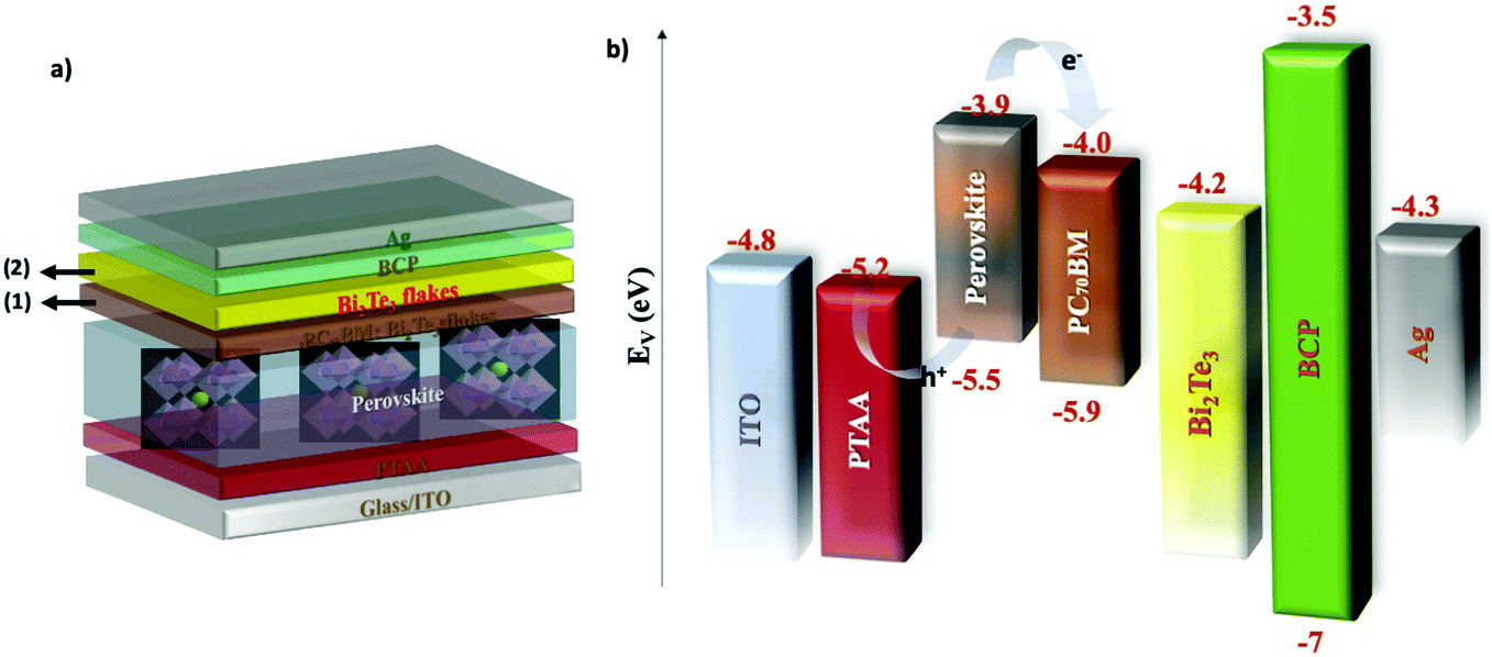 | ||
| Fig. 2 (a) Schematic illustration (not to scale) of a typical inverted p–i–n perovskite device consisting of the following material stack: glass/ITO/PTAA/perovskite/PC70BM/BCP/Ag. A two-fold engineering approach is implemented by doping the ETL, PC70BM (position 1), with Bi2Te3 flakes (flake dispersion in CB) and by forming an interlayer on top of the ETL (position 2) using multiple spin coatings of Bi2Te3 flakes (pristine flake dispersion in IPA:ACN). (b) A graphical presentation of the material stack energy levels. | ||
Hereafter, the cells using pristine PC70BM are named PSC-Ref. The cells using doped PC70BM are named PSC-Dop2 and PSC-Dop3 for Bi2Te3 flake dispersion doping of the PC70BM solution of 2% and 3% v/v, respectively. The cells incorporating the Bi2Te3 interlayer are named PSC-Int1, PSC-Int2 and PSC-Int3 having an interlayer respectively formed by 1 SC, 2 SCs and 3 SCs of the Bi2Te3 flake dispersion onto PC70BM. Finally, the cells incorporating both engineering approaches are named PSC-Com1, PSC-Com2 and PSC-Com3, having an interlayer formed by 1 SC, 2 SCs and 3 SCs, respectively, while all incorporating 2% v/v PC70BM doping.
Representative top-view and cross-section SEM images of the PSC-Ref are presented in Fig. 3a and b respectively. In particular, Fig. 3a shows the perovskite surface, evidencing crystal grain sizes of approximately 250 nm. Fig. 3b depicts a typical cross-section of a complete reference device, nicely showing its layered structure. Top-view and cross-section SEM images of PSC-Com2 are shown in Fig. 3c and d, respectively. Notably, since most of the flakes have thicknesses around 3 nm or below (see TEM and AFM data in Fig. 1), only the thicker Bi2Te3 flakes can be detected by the SEM imaging shown in Fig. 3c. However, SEM-EDX analysis (Fig. S4, ESI†) and AFM measurements (Fig. S5, ESI†) confirmed the presence of Bi2Te3 flakes on the PC70BM surface, as well as inside the doped PC70BM (Fig. S6a, ESI†). The Bi2Te3 interlayer positioned on the PC70BM surface passivates shunt pathways by covering both cracks and pinholes (for details see the extended discussion regarding the J–V analysis in the next section). Moreover, the Bi2Te3 flake doping does not affect the morphology of the PC70BM, which is similar to the one reported in previous work.19 Finally, as shown by the cross-sectional SEM imaging (Fig. 3d), the insertion of the Bi2Te3 interlayer does not affect the device morphology, indicating that the solvent (CB) used to disperse the Bi2Te3 flakes is compatible with both the PC70BM and the perovskite layer. A perovskite layer thickness of approximately 400 nm is determined for both device types.
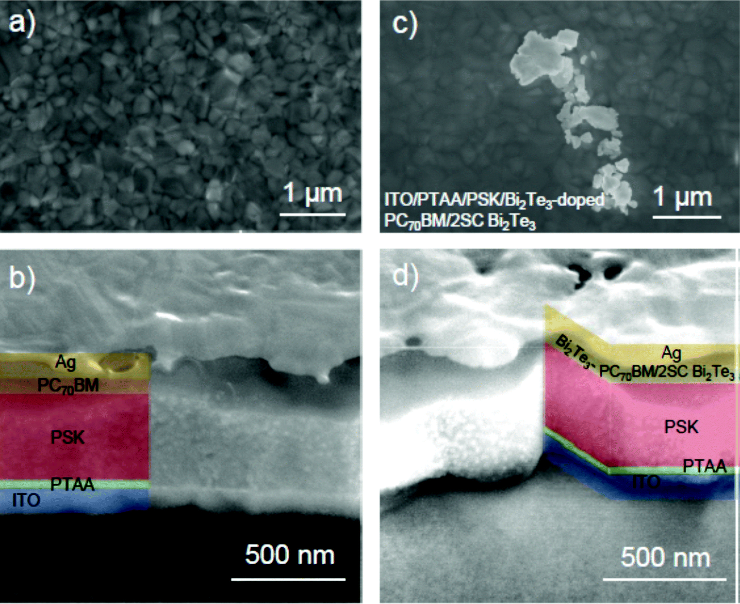 | ||
| Fig. 3 Representative top view and cross-section SEM images of PSC-Ref (panels (a) and (b)) and PSC-Com2 (panels (c) and (d)). (a) Top view of the perovskite surface prior to PC70BM deposition in PSC-Ref. (b) Cross-section SEM image of PSC-Ref. (c) Top view of the interlayer surface in PSC-Com2. (d) Cross-section SEM image of PSC-Com2. False colouring was used for the different layers of the structure: ITO/PTAA/perovskite (PSK)/PC70BM/Ag. For clarity the top view SEM images were collected in areas outside of the contacts and in the case of the reference before the PC70BM coating. | ||
Steady state photovoltaic characterization of PSC devices
The photovoltaic performance of the PSCs was initially evaluated by incorporating different levels of Bi2Te3 doping in the PC70BM ETL. As shown in Fig. 4a, the optimal photovoltaic performance was achieved for 2% v/v doping, namely PSC-Dop2. In detail, the incorporation of Bi2Te3 flakes increased the PCE of the champion devices from 16.89% (PSC-Ref) to 18.0%, corresponding to a ∼6.6% enhancement (see Table 1). However, by further increasing the amount of doping to 3% v/v (PSC-Dop3), the PCE decreased to 17.4%. Nevertheless, this value is still superior to the reference cell.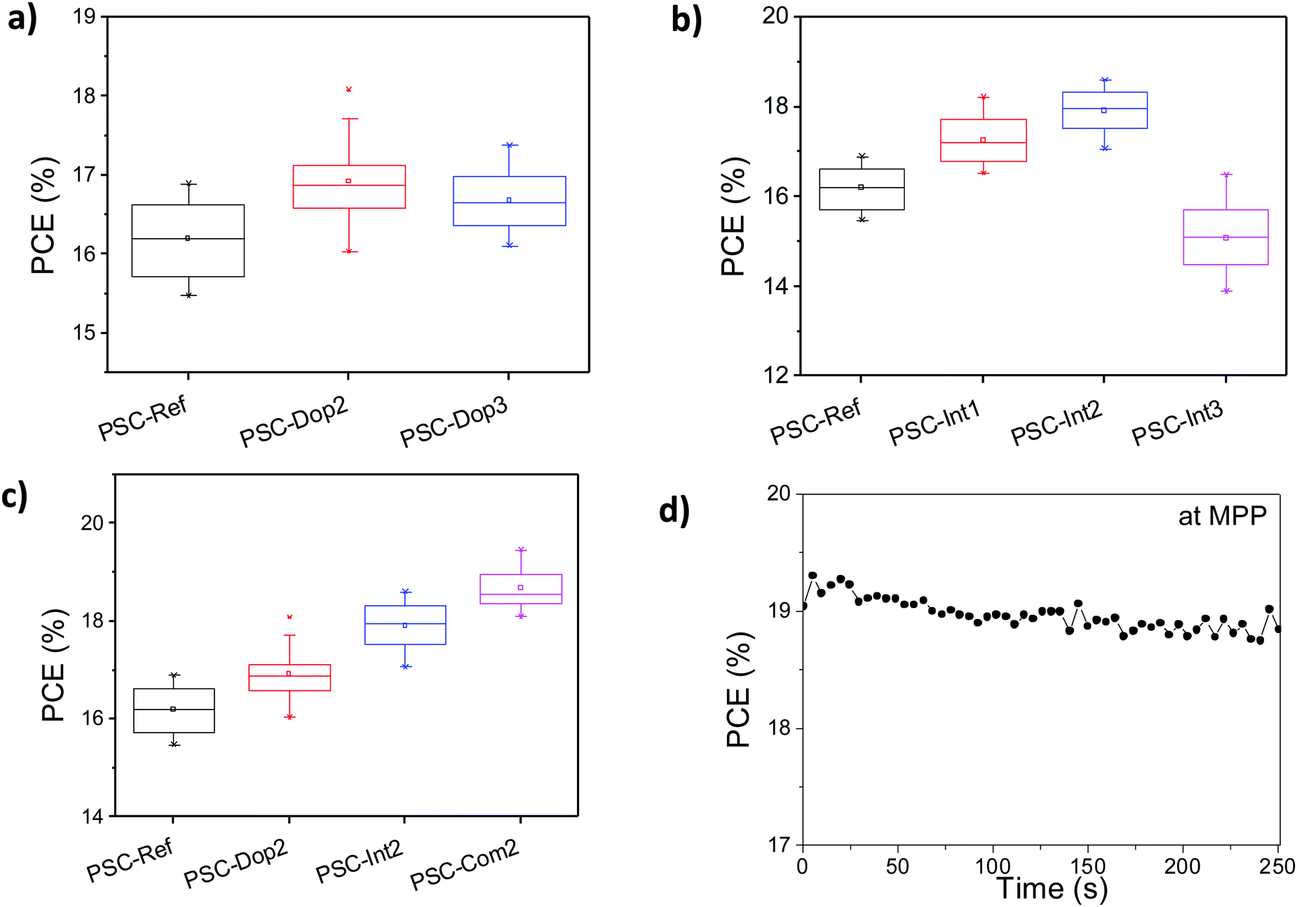 | ||
| Fig. 4 Device performance statistics of each engineering approach implemented separately or combined for various material conditions. (a) Device performance statistics of PSC-Ref (black), PSC-Dop2 (red) and PSC-Dop3 (blue). (b) Device performance statistics of PSC-Ref (black), PSC-Int1 (red), PSC-Int2 (blue) and PSC-Int3 (purple). The number of SCs was 1, 2 and 3, respectively. (c) Device performance statistics of PSC-Dop2 (red), PSC-Int2 (blue), and PSC-Com2 (purple). (d) Maximum power point tracking plot of PSC-Com2 for 250 s showing enhanced stability of the steady state PCE. | ||
| Device | PCE (%) | V oc (V) | FF | J sc (mA cm2) | R sh (Ohm cm−2) | R s (Ohm cm−2) | ||||||
|---|---|---|---|---|---|---|---|---|---|---|---|---|
| PSC-Ref | 16.86 | 16.78 | 1.071 | 1.074 | 0.739 | 0.732 | 21.49 | 21.34 | 225 | 763 | 4.56 | 4.50 |
| PSC-Dop2 | 18.01 | 17.84 | 1.115 | 1.115 | 0.757 | 0.735 | 21.42 | 21.27 | 262 | 935 | 4.61 | 4.67 |
| PSC-Int2 | 18.60 | 18.57 | 1.10 | 1.10 | 0.763 | 0.766 | 22.18 | 22.04 | 277 | 337 | 4.27 | 4.26 |
| PSC-Com2 | 19.46 | 19.28 | 1.096 | 1.096 | 0.788 | 0.783 | 22.52 | 22.46 | 696 | 1390 | 3.87 | 3.87 |
| FS | RS | FS | RS | FS | RS | FS | RS | FS | RS | FS | RS | |
A similar investigation was performed by tuning the number of consecutive SCs (from 0 up to 3) of the Bi2Te3 flake dispersion in IPA:ACN on top of the undoped PC70BM (Fig. 4b). The maximum photovoltaic performance was achieved after 2 consecutive SCs (PSC-Int2), resulting in a PCE as high as 18.6% (+10% vs. PSC-Ref). The further increase of the number of SCs to 3 (PSC-Int3) significantly reduced the photovoltaic performance, resulting in a PCE close to 15%. This behaviour is likely due to the enhanced electron scattering rate as the interlayer thickness increases,38,49 as well as to the possible negative effect of the excessive exposure of the underlying layers to IPA:ACN solvent (see SEM analysis in Fig. S6b and c, ESI†). Although the simplicity of spin coating deposition is effective for preliminary lab-scale studies, the use of automated methods to deposit 2D material based inks on a large scale, e.g., spray coating, could overcome any issue related to the spin coating deposition of Bi2Te3 flakes and further increase the current device performance.
Upon identifying separately the optimal conditions for each engineering approach, we then combined both the above discussed strategies into a single PSC (PSC-Com cells). This led to PSC devices exhibiting PCE values up to 19.46% (PSC-Com2 in Fig. 4c), corresponding to a significant +15.2% enhancement compared to the values measured for PSC-Ref. In addition, Fig. 4c also reports the device performance statistics for PSC-Dop2 and PSC-Int2, i.e., the cells obtained through the single engineering approach at optimum conditions, together with those for PSC-Ref. Moreover, the J–V curves of the champion devices of PSC-Dop2, PSC-Int2 and PSC-Com2 are presented in Fig. 5a, in comparison with the one measured for the PSC-Ref champion. Table 1 summarizes the main device photovoltaic parameters extracted from the J–V curves, i.e., the PCE, the Voc, the Jsc and the fill factor (FF). All devices exhibited negligible hysteresis as proved by Fig. S7 (ESI†), where forward and reverse J–V scans are presented, and by Table 1, where all device characteristics are listed. Moreover, the steady-state PCE behaviour of the devices was excellent as shown in Fig. 4d, where the maximum power point tracking plot of the PSC-Com2 PCE for 250 s is depicted (below 1% difference).
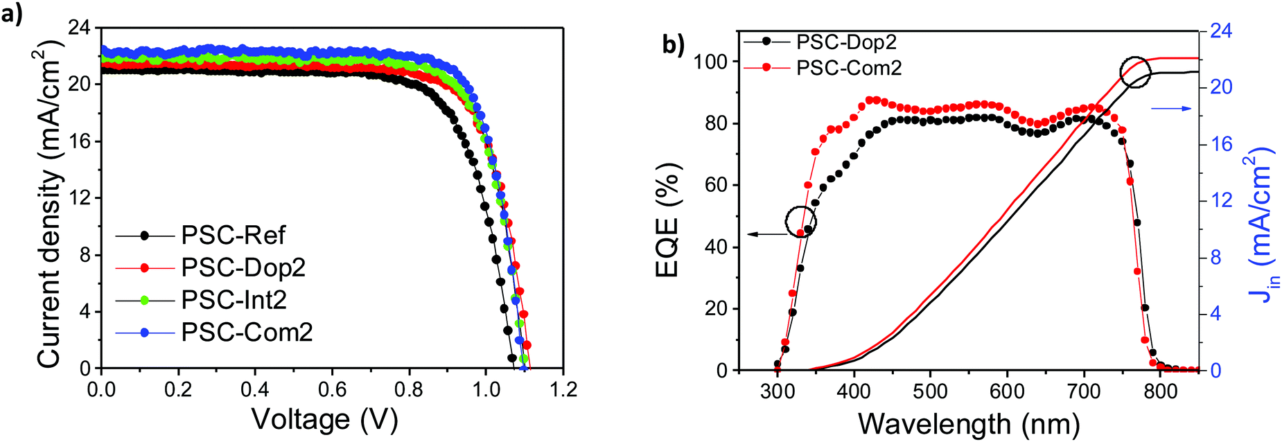 | ||
| Fig. 5 J–V characteristics at 1 sun illumination of each engineering approach and the EQE spectrum of a representative device. (a) J–V curves of PSC-Ref (black), PSC-Dop2 (red), PSC-Int2 (green), and PSC-Com2 (blue). (b) Representative EQE of PSC-Int2 and PSC-Com2. The integrated current density of the device's spectral response with the AM1.5G photon flux spectrum is depicted on the right axis. | ||
Fig. 5b displays the EQE spectrum of representative PSC-Int2 and PSC-Com2 devices. The EQE curves show a wide photoresponse in a spectral region from 300 to 830 nm, which is consistent with the absorption spectrum of the perovskite film.51 From the high-wavelength edge of the EQE spectrum, the band gap of the perovskite is estimated to be ∼1.6 eV. The integrated current densities for PSC-Int2 and PSC-Com2 are 21.01 and 22 mA cm−2, respectively, which deviate by less than 3% compared to the Jsc values measured in the J–V curve (Fig. 5a).
Photoluminescence (PL) measurements were also performed to support the role of the Bi2Te3 flakes in improving the performance of the PSCs. It is noteworthy that PL analysis represents an effective tool to qualitatively detect changes of carrier extraction rates at the various interfaces of PSCs.19,50,51 As shown in Fig. S8 (ESI†), our PL measurements corroborate the beneficial role of Bi2Te3 flakes acting either as an ETL dopant or as an interlayer in inverted PSCs. Indeed, although significant quenching of the PL intensity occurs after the deposition of the PC70BM layer on top of the perovskite (inset of Fig. S8, ESI†), the maximum PL quenching is observed in PSC-Com2. Therefore, these data clearly indicate that PSC-Com2 shows optimal charge extraction, in agreement with its highest photovoltaic performance among those measured for the investigated PSCs.
In summary, with the incorporation of Bi2Te3 flakes either as PC70BM dopants or as an interlayer, the photovoltaic performance can be significantly improved, suggesting an active role of the flakes to enhance the electron extraction dynamics. In particular, the Bi2Te3-based PSCs exhibited higher Voc, Jsc and FF values compared to the reference cell as a direct consequence of: (1) the favourable energetic alignment between the LUMO of the PC70BM and the WF of the Ag in the presence of the Bi2Te3 flakes, and (2) the enhanced carrier extraction induced by conductive paths within the PC70BM layer originating from the surface states of the Bi2Te3 flakes.72
Transient photovoltage characterization of PSCs
Transient photovoltage and TPC measurements were performed to further support the physical mechanism of the reported performance enhancement when the Bi2Te3 flakes were incorporated into the PSCs. Fig. 6a shows the comparison between the photovoltage decay curves of PSC-Int2, PSC-Com2 and PSC-Ref. Small perturbation TPV decays followed a single exponential trend, which can result from either charge carrier annihilation or three-body recombination. Since the excitons in perovskites dissociate after 2 ps upon generation and our measurements cover a μs-scale, we can safely disregard the potential exciton contribution. Hence, the measured decay curves are a consequence of electron–hole recombination, and the transient tail can directly yield the carrier lifetimes. The data indicate that the devices incorporating Bi2Te3 flakes exhibit a Voc decay slower than the one of the reference device. In particular, TPV results show that the Bi2Te3 flakes reduce the charge recombination rate and increase the charge carrier lifetime (Fig. 6b), which is consistent with the highest Voc of Bi2Te3-based devices measured through the J–V characterization (see Fig. 5a and Table 1). Furthermore, the addition of the Bi2Te3 flakes does not significantly affect the distribution of shallow defect states, as seen from the voltage rise times shown in the inset of Fig. S9 (ESI†) (panels a to d), clearly demonstrating a negligible change between the reference and the Bi2Te3-based PSCs. On the other hand, the PSC-Int2 and PSC-Com2 devices are less sensitive to capacitive contributions (low bias conditions in Fig. S9, ESI†). This is due to the spatially divided distribution of charge carriers and shunt pathways, which means that the Bi2Te3-based PCSs are less affected by electrically injected/background carriers. Transient photocurrent experiments in charge extraction mode demonstrated that the use of Bi2Te3 flakes increases the overall extracted charge density, especially in the PSC-Com2 device (blue data in Fig. 6c). This data suggests that the metallic character of the Bi2Te3 flakes improves the charge extraction efficiency. The measurements performed in the high perturbation regime (0.8 duty cycle) show the absence of deep trap states in all the tested samples (see ESI† TPC data in Fig. S10). By doping the PC70BM with the Bi2Te3 flakes, the charge transport was slightly slowed down, as evidenced by the calculated transit times (Fig. 6d), obtained under low perturbation conditions. However, this is compensated in the optimal device case (PSC-Com2 device), which showed a higher extraction rate compared to the reference device. The extrapolated charge carrier transfer times are on the order of 10−7 s in all the investigated devices. These values are about ten times higher than the bimolecular recombination lifetime measured by TPV (tens of μs). Therefore, we can reasonably assume that the charge recombination and extraction processes are non-competitive, which is consistent with the high PCE achieved by our PSCs.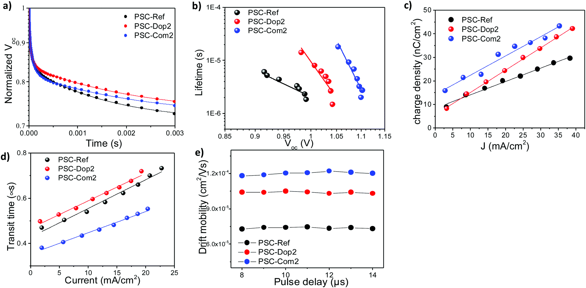 | ||
| Fig. 6 Estimation of the carrier lifetime, device extracted charge density and transit time, as well as the effective carrier mobility, based on transient measurements. (a) Normalized Voc decay of PSC-Ref (black), PSC-Dop2 (red) and PSC-Com2 (blue). The lines represent fittings with an exponential decay function. (b) Extracted corresponding lifetimes from TPV decay measurements at different bias conditions. (c) Charge density and (d) transit time extracted from TPC measurements. The lines in panels (b–d) represent linear fittings. (e) Drift mobility estimation from the photo-CELIV technique. | ||
The drift mobility of electrons/holes was probed using charge extraction by linearly increasing voltage (photo-CELIV) under various light pulse delay points. In detail, the drift mobility was derived from the extracted charge represented by the part of the transient superimposed over the displacement current level (Fig. S11, ESI†). Taking into account the fact that perovskites are not highly disordered materials, according to the equation proposed by Lorrmann et al. the mobility can be derived as:73

Lifetime stability measurements of PSCs
The stability of the PSCs is also a crucial performance parameter for addressing typical commercial standards in photovoltaic technologies. Several reports have identified oxygen and moisture as external degradation agents along with the diffusion of metal species from the top electrode towards the perovskite layer and the escape of organic molecules from the perovskite crystal.68,69 Hereby, the evaluation of the lifetime of the investigated PSCs was performed by implementing the ISOS-L2 protocol, in which the samples are tested under continuous 1 sun illumination at a temperature above 65 °C. As shown in Fig. 7a, the PCE of PSC-Ref exhibited a drop of its initial PCE by 50% after 15 h (T50), and below 20% after 100 h. PSC-Int1 reported a moderate stability performance, showing a lifetime T50 of ca. 70 h. Notably, PSC-Int2 significantly improved the device stability, displaying a T70 superior to 600 h. The stability of PSC-Int2 can be explained by the optimal coverage of the PC70BM with the Bi2Te3 flake interlayer optimized in its thickness. It has been already reported that the PC70BM is the main path for the migration of the metal species towards the perovskite.74,75 We attribute the exceptional stability of PSC-Int2 to the Bi2Te3 interlayer, which passivates the PC70BM pin-holes and its imperfections. The Bi2Te3 interlayer acts as a barrier for the Ag ion migration towards the perovskite, and it also suppresses the escape rate of both cations and anions from the perovskite (mainly MA).72 On the other hand, the PSC-Int3 device exhibited enhanced stability compared to the reference, retaining 40% of its initial PCE after 400 h. However, its stability was lower than the PSC-Int2 device. This can be attributed to the washing out of the previously formed films when the number of consecutive SCs exceeds two, and/or the negative impact of the solvent of the Bi2Te3 flake dispersion over the underlying PC70BM and perovskite layers.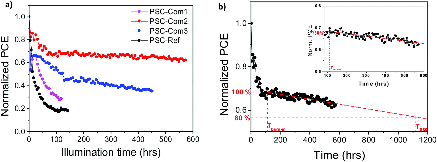 | ||
| Fig. 7 (a) Long term ISOS-L2 stability measurements of PSC-Ref (black), PSC-Com1 (purple), PSC-Com2 (red) and PSC-Com3 (blue). (b) Further analysis of the long term stability measurement of PSC-Com2. All the devices were encapsulated. The red line is a linear fit of the experimental points in the stabilized region extrapolated to 1200 h. Tburn-in marks the end of the burn-in phase and Ts80 denotes the time at which the initial PCE has dropped by 20% in the stabilized region. The inset shows the linear region of the lifetime measurements. | ||
A typical lifetime stability measurement of the best performing PSCs-Int2 reveals a burn-in phase lasting for about 100 h. During this phase, the device retained 70% of its initial PCE. Thereafter, a stabilized behaviour is followed by a slow linear drop. In accordance with the updated ISOS protocols that specifically address the testing protocol for PCSs,76 the time at the end of the burn-in phase can be noted as Tburn-in, while the time at which the PCE has dropped by 20% compared to this value is referred to as Ts80. A linear fit was performed in the temporal region corresponding to a stable PSC behaviour, enabling the estimation of the degradation rate. The degradation slope was found to be −0.017% PCE h−1. Conversely, following this approach we estimated Ts80 to be approximately 1100 h under continuous 1 sun illumination.
Conclusions
Ultrathin flakes of Bi2Te3 were produced through the LPE method to be incorporated via solution-processing techniques in two distinct positions across inverted planar PSCs. In particular, the Bi2Te3 flakes were evaluated as dopants of the PC70BM and as an interlayer between the PC70BM and the Ag. The combination of these two engineering approaches led to an increase of both the device efficiency and stability. The optimal doping of PC70BM with Bi2Te3 flakes was found to be 2% v/v, which resulted in a PCE of 18.0%. This value corresponds to an increase of 6.6% compared to the values measured for the reference device. An optimal interlayer was achieved by performing 2 SCs of the Bi2Te3 flake dispersion onto the PC70BM, leading to a PCE of 18.6%. This value corresponds to a 10% improvement, while this protective interlayer notably enhanced the stability and lifetime of the devices under ISOS-L2 protocols. By combining these two engineering approaches, PCE values of champion devices (PSC-Com2) were reported up to 19.46%, corresponding to an improvement of 15.2% compared to the reference device. Furthermore, the PSC-Com2 device retained 80% of its initial PCE, after the burn in phase, for more than 1100 h, resulting in one of the highest stability performances reported for inverted PSCs to date. Transient transport measurements, and structural and optical characterization supported the observation that this combined engineering approach increases the carrier lifetimes, the extracted charge density and the carrier effective mobilities.Conflicts of interest
There are no conflicts to declare.Acknowledgements
The work has been supported by European Union's Horizon 2020 research and innovation program under grant agreements No. 785219 – GrapheneCore2 and 881603 – GrapheneCore3. We thank Electron Microscopy facility – Istituto Italiano di Tecnologia for the support in TEM data acquisition.Notes and references
- A. S. R. Bati, M. Batmunkh and J. G. Shapter, Adv. Energy Mater., 2019, 1902253 Search PubMed.
- S. Das, D. Pandey, J. Thomas and T. Roy, Adv. Mater., 2019, 31, 1802722 CrossRef PubMed.
- G. Kakavelakis, E. Kymakis and K. Petridis, Adv. Mater. Interfaces, 2018, 5, 1800339 CrossRef.
- M. Petrović, K. Rogdakis and E. Kymakis, J. Phys.: Energy, 2019, 1, 044001 Search PubMed.
- C. Li, Q. Cao, F. Wang, Y. Xiao, Y. Li, J.-J. Delaunay and H. Zhu, Chem. Soc. Rev., 2018, 47, 4981–5037 RSC.
- F. Yi, H. Ren, J. Shan, X. Sun, D. Wei and Z. Liu, Chem. Soc. Rev., 2018, 47, 3152–3188 RSC.
- S. Lee, Q. Shi and C. Lee, APL Mater., 2019, 7, 031302 CrossRef.
- T. R. Ray, J. Choi, A. J. Bandodkar, S. Krishnan, P. Gutruf, L. Tian, R. Ghaffari and J. A. Rogers, Chem. Rev., 2019, 119, 5461–5533 CrossRef CAS PubMed.
- F. Bonaccorso, A. Bartolotta, J. N. Coleman and C. Backes, Adv. Mater., 2016, 28, 6136–6166 CrossRef CAS PubMed.
- C. Backes, et al. , 2D Mater., 2020, 7, 022001 CrossRef.
- S. Bellani, E. Petroni, A. E. Del Rio Castillo, N. Curreli, B. Martín-García, R. Oropesa-Nuñez, M. Prato and F. Bonaccorso, Adv. Funct. Mater., 2019, 29, 1807659 CrossRef.
- X. Zhao, S. Liu, H. Zhang, S.-Y. Chang, W. Huang, B. Zhu, Y. Shen, C. Shen, D. Wang, Y. Yang and M. Wang, Adv. Funct. Mater., 2019, 29, 1805168 CrossRef.
- L. Yang, Y. Dall’Agnese, K. Hantanasirisakul, C. E. Shuck, K. Maleski, M. Alhabeb, G. Chen, Y. Gao, Y. Sanehira, A. K. Jena, L. Shen, C. Dall’Agnese, X.-F. Wang, Y. Gogotsi and T. Miyasaka, J. Mater. Chem. A, 2019, 7, 5635–5642 RSC.
- L. Najafi, B. Taheri, B. Martín-García, S. Bellani, D. Di Girolamo, A. Agresti, R. Oropesa-Nuñez, S. Pescetelli, L. Vesce, E. Calabrò, M. Prato, A. E. Del Rio Castillo, A. Di Carlo and F. Bonaccorso, ACS Nano, 2018, 12, 10736–10754 CrossRef CAS PubMed.
- P. O’Keeffe, D. Catone, A. Paladini, F. Toschi, S. Turchini, L. Avaldi, F. Martelli, A. Agresti, S. Pescetelli, A. E. Del Rio Castillo, F. Bonaccorso and A. Di Carlo, Nano Lett., 2019, 19, 684–691 CrossRef PubMed.
- B. Taheri, N. Yaghoobi Nia, A. Agresti, S. Pescetelli, C. Ciceroni, A. E. Del Rio Castillo, L. Cinà, S. Bellani, F. Bonaccorso and A. Di Carlo, 2D Mater., 2018, 5, 045034 CrossRef CAS.
- P. Huang, Q. Chen, K. Zhang, L. Yuan, Y. Zhou, B. Song and Y. Li, J. Mater. Chem. A, 2019, 7, 6213–6219 RSC.
- G. Tang, P. You, Q. Tai, A. Yang, J. Cao, F. Zheng, Z. Zhou, J. Zhao, P. K. L. Chan and F. Yan, Adv. Mater., 2019, 31, 1807689 CrossRef PubMed.
- G. Kakavelakis, I. Paradisanos, B. Paci, A. Generosi, M. Papachatzakis, T. Maksudov, L. Najafi, A. E. Del Rio Castillo, G. Kioseoglou, E. Stratakis, F. Bonaccorso and E. Kymakis, Adv. Energy Mater., 2018, 8, 1702287 CrossRef.
- E. Lamanna, F. Matteocci, E. Calabrò, L. Serenelli, E. Salza, L. Martini, F. Menchini, M. Izzi, A. Agresti, S. Pescetelli, S. Bellani, A. E. Del Río Castillo, F. Bonaccorso, M. Tucci and A. D. Carlo, Joule, 2020, 4, 865 CrossRef CAS.
- A. Agresti, S. Pescetelli, A. L. Palma, B. Martín-García, L. Najafi, S. Bellani, I. Moreels, M. Prato, F. Bonaccorso and A. Di Carlo, ACS Energy Lett., 2019, 4, 1862–1871 CrossRef CAS.
- A. Agresti, A. Pazniak, S. Pescetelli, A. Di Vito, D. Rossi, A. Pecchia, M. Auf der Maur, A. Liedl, R. Larciprete, D. V. Kuznetsov, D. Saranin and A. Di Carlo, Nat. Mater., 2019, 18, 1228–1234 CrossRef CAS PubMed.
- M. Batmunkh, K. Vimalanathan, C. Wu, A. S. R. Bati, L. Yu, S. A. Tawfik, M. J. Ford, T. J. Macdonald, C. L. Raston, S. Priya, C. T. Gibson and J. G. Shapter, Small Methods, 2019, 3, 1800521 CrossRef.
- W. Chen, K. Li, Y. Wang, X. Feng, Z. Liao, Q. Su, X. Lin and Z. He, J. Phys. Chem. Lett., 2017, 8, 591–598 CrossRef CAS PubMed.
- F. Zhang, J. He, Y. Xiang, K. Zheng, B. Xue, S. Ye, X. Peng, Y. Hao, J. Lian, P. Zeng, J. Qu and J. Song, Adv. Mater., 2018, 30, 1803244 CrossRef PubMed.
- S. Das, D. Pandey, J. Thomas and T. Roy, Adv. Mater., 2019, 31, 1802722 CrossRef PubMed.
- X. Zhao, S. Liu, H. Zhang, S.-Y. Chang, W. Huang, B. Zhu, Y. Shen, C. Shen, D. Wang, Y. Yang and M. Wang, Adv. Funct. Mater., 2019, 29, 1805168 CrossRef.
- E. Singh, K. S. Kim, G. Y. Yeom and H. S. Nalwa, ACS Appl. Mater. Interfaces, 2017, 9, 3223–3245 CrossRef CAS PubMed.
- S. Kohnehpoushi, P. Nazari, B. A. Nejand and M. Eskandari, Nanotechnology, 2018, 29, 205201 CrossRef PubMed.
- A. E. Del Rio Castillo, V. Pellegrini, A. Ansaldo, F. Ricciardella, H. Sun, L. Marasco, J. Buha, Z. Dang, L. Gagliani, E. Lago, N. Curreli, S. Gentiluomo, F. Palazon, M. Prato, R. Oropesa-Nuñez, P. S. Toth, E. Mantero, M. Crugliano, A. Gamucci, A. Tomadin, M. Polini and F. Bonaccorso, Mater. Horiz., 2018, 5, 890–904 RSC.
- Y. Guo, S. Zhou, Y. Bai and J. Zhao, ACS Appl. Mater. Interfaces, 2017, 9, 12013–12020 CrossRef CAS PubMed.
- S. Chen, L. Brown, M. Levendorf, W. Cai, S.-Y. Ju, J. Edgeworth, X. Li, C. W. Magnuson, A. Velamakanni, R. D. Piner, J. Kang, J. Park and R. S. Ruoff, ACS Nano, 2011, 5, 1321–1327 CrossRef CAS PubMed.
- Y. Choi, S. Jung, N. K. Oh, J. Lee, J. Seo, U. Kim, D. Koo and H. Park, ChemNanoMat, 2019, 5, 1050–1058 CrossRef CAS.
- J. He, F. Zhang, Y. Xiang, J. Lian, X. Wang, Y. Zhang, X. Peng, P. Zeng, J. Qu and J. Song, J. Power Sources, 2019, 435, 226819 CrossRef CAS.
- X. Zhang, G. Ji, D. Xiong, Z. Su, B. Zhao, K. Shen, Y. Yang and X. Gao, RSC Adv., 2018, 8, 987–993 RSC.
- Z. Guo, L. Gao, Z. Xu, S. Teo, C. Zhang, Y. Kamata, S. Hayase and T. Ma, Small, 2018, 14, 1802738 CrossRef PubMed.
- N. Arora, M. I. Dar, A. Hinderhofer, N. Pellet, F. Schreiber, S. M. Zakeeruddin and M. Grätzel, Science, 2017, 358, 768–771 CrossRef CAS PubMed.
- S. Wu, R. Chen, S. Zhang, B. H. Babu, Y. Yue, H. Zhu, Z. Yang, C. Chen, W. Chen, Y. Huang, S. Fang, T. Liu, L. Han and W. Chen, Nat. Commun., 2019, 10, 1161 CrossRef PubMed.
- J. E. Moore, Nature, 2010, 464, 194–198 CrossRef CAS PubMed.
- D. N. Basov, R. D. Averitt and D. Hsieh, Nat. Mater., 2017, 16, 1077–1088 CrossRef CAS PubMed.
- Y.-Y. Li, G. Wang, X.-G. Zhu, M.-H. Liu, C. Ye, X. Chen, Y.-Y. Wang, K. He, L.-L. Wang, X.-C. Ma, H.-J. Zhang, X. Dai, Z. Fang, X.-C. Xie, Y. Liu, X.-L. Qi, J.-F. Jia, S.-C. Zhang and Q.-K. Xue, Adv. Mater., 2010, 22, 4002–4007 CrossRef CAS PubMed.
- X. Chen, Z.-X. Liu and X.-G. Wen, Phys. Rev. B: Condens. Matter Mater. Phys., 2011, 84, 235141 CrossRef.
- H. Zhang, C.-X. Liu, X.-L. Qi, X. Dai, Z. Fang and S.-C. Zhang, Nat. Phys., 2009, 5, 438–442 Search PubMed.
- T. Cheng, H. Lang, Z. Li, Z. Liu and Z. Liu, Phys. Chem. Chem. Phys., 2017, 19, 23942–23950 RSC.
- V. Raman, D. Punnoose, P. Baraneedharan, S. S. Rao, C. V. V. M. Gopi, V. S. S. Brahadeeswaran and H.-J. Kim, RSC Adv., 2017, 7, 6735–6742 RSC.
- T. Chen, G. H. Guai, C. Gong, W. Hu, J. Zhu, H. Yang, Q. Yan and C. M. Li, Energy Environ. Sci., 2012, 5, 6294–6298 RSC.
- M. Wang, Q. Fu, L. Yan, W. Pi, G. Wang, Z. Zheng and W. Luo, ACS Appl. Mater. Interfaces, 2019, 11, 47868–47877 CrossRef CAS PubMed.
- L. Fu, Y. Nie, B. Li, N. Li, B. Cao and L. Yin, Sol. RRL, 2019, 3, 1900233 CrossRef CAS.
- M. Wang, Q. Fu, L. Yan, W. Pi, G. Wang, Z. Zheng and W. Luo, ACS Appl. Mater. Interfaces, 2019, 11, 47868–47877 CrossRef CAS PubMed.
- G. Kakavelakis, A. E. Del Rio Castillo, V. Pellegrini, A. Ansaldo, P. Tzourmpakis, R. Brescia, M. Prato, E. Stratakis, E. Kymakis and F. Bonaccorso, ACS Nano, 2017, 11, 3517–3531 CrossRef CAS PubMed.
- M. Saliba, T. Matsui, K. Domanski, J. Y. Seo, A. Ummadisingu, S. M. Zakeeruddin, J. P. Correa-Baena, W. R. Tress, A. Abate, A. Hagfeldt and M. Grätzel, Science, 2016, 354, 206–209 CrossRef CAS PubMed.
- E. Carroll, D. Buckley, N. V. V. Mogili, D. McNulty, M. S. Moreno, C. Glynn, G. Collins, J. D. Holmes, K. M. Razeeb and C. O’Dwyer, Chem. Mater., 2017, 29, 7390–7400 CrossRef CAS.
- G. Jiang, J. Yi, L. Miao, P. Tang, H. Huang, C. Zhao and S. Wen, Sci. Rep., 2018, 8, 2355 CrossRef PubMed.
- D. Teweldebrhan, V. Goyal and A. A. Balandin, Nano Lett., 2010, 10, 1209–1218 CrossRef CAS PubMed.
- D. Kong, W. Dang, J. J. Cha, H. Li, S. Meister, H. Peng, Z. Liu and Y. Cui, Nano Lett., 2010, 10, 2245–2250 CrossRef CAS PubMed.
- K. M. F. Shahil, M. Z. Hossain, D. Teweldebrhan and A. A. Balandin, Appl. Phys. Lett., 2010, 96, 153103 CrossRef.
- V. Russo, A. Bailini, M. Zamboni, M. Passoni, C. Conti, C. S. Casari, A. Li Bassi and C. E. Bottani, J. Raman Spectrosc., 2008, 39, 205–210 CrossRef CAS.
- Y. Zhao, R. W. Hughes, Z. Su, W. Zhou and D. H. Gregory, Angew. Chem., Int. Ed., 2011, 50, 10397–10401 CrossRef CAS PubMed.
- K. M. F. Shahil, M. Z. Hossain, V. Goyal and A. A. Balandin, J. Appl. Phys., 2012, 111, 054305 CrossRef.
- L. Chen, Q. Zhao and X. Ruan, Mater. Lett., 2012, 82, 112–115 CrossRef CAS.
- X. Qi, W. Ma, X. Zhang and C. Zhang, Appl. Surf. Sci., 2018, 457, 41–48 CrossRef CAS.
- L. Ren, X. Qi, Y. Liu, G. Hao, Z. Huang, X. Zou, L. Yang, J. Li and J. Zhong, J. Mater. Chem., 2012, 22, 4921 RSC.
- S. Liu, X. F. Lu, J. Xiao, X. Wang and X. W. Lou, Angew. Chem., Int. Ed., 2019, 58, 13828–13833 CrossRef CAS PubMed.
- L. Miao, J. Yi, Q. Wang, D. Feng, H. He, S. Lu, C. Zhao, H. Zhang and S. Wen, Opt. Mater. Express, 2016, 6, 2244 CrossRef CAS.
- L. Sun, Z. Lin, J. Peng, J. Weng, Y. Huang and Z. Luo, Sci. Rep., 2015, 4, 4794 CrossRef PubMed.
- Y. He and Y. Li, Phys. Chem. Chem. Phys., 2011, 13, 1970–1983 RSC.
- M. Uda, A. Nakamura, T. Yamamoto and Y. Fujimoto, J. Electron Spectrosc. Relat. Phenom., 1998, 88–91, 643–648 CrossRef CAS.
- C. C. Boyd, R. Cheacharoen, T. Leijtens and M. D. McGehee, Chem. Rev., 2019, 119, 3418–3451 CrossRef CAS PubMed.
- Y. Zhao, W. Zhou, H. Tan, R. Fu, Q. Li, F. Lin, D. Yu, G. Walters, E. H. Sargent and Q. Zhao, J. Phys. Chem. C, 2017, 121, 14517–14523 CrossRef CAS.
- E. Bi, H. Chen, F. Xie, Y. Wu, W. Chen, Y. Su, A. Islam, M. Grätzel, X. Yang and L. Han, Nat. Commun., 2017, 8, 15330 CrossRef CAS PubMed.
- Y. Wang, T. Wu, J. Barbaud, W. Kong, D. Cui, H. Chen, X. Yang and L. Han, Science, 2019, 365, 687–691 CrossRef CAS PubMed.
- C. C. Boyd, R. Cheacharoen, K. A. Bush, R. Prasanna, T. Leijtens and M. D. McGehee, ACS Energy Lett., 2018, 3, 1772–1778 CrossRef CAS.
- J. Lorrmann, B. H. Badada, O. Inganäs, V. Dyakonov and C. Deibel, J. Appl. Phys., 2010, 108, 113705 CrossRef.
- J. Min, Z. G. Zhang, Y. Hou, C. O. R. Quiroz, T. Przybilla, C. Bronnbauer, F. Guo, K. Forberich, H. Azimi, T. Ameri, E. Spiecker, Y. Li and C. J. Brabec, Chem. Mater., 2015, 27, 227–234 CrossRef CAS.
- S. S. Mali, H. Kim, H. H. Kim, S. E. Shim and C. K. Hong, Mater. Today, 2018, 21, 483–500 CrossRef CAS.
- M. V. Khenkin, et al. , Nat. Energy, 2020, 5, 35–49 CrossRef.
Footnote |
| † Electronic supplementary information (ESI) available: UV-vis-NIR absorption measurement of the Bi2Te3 flakes and Tauc analysis, SEM/EDX analysis and AFM topography images of the doped PCMB and PCBM surface with/without 2D material incorporation, and PL data as well as raw TPV, TPC and photo-Celiv data. See DOI: 10.1039/d0ma00162g |
| This journal is © The Royal Society of Chemistry 2020 |