
 Open Access Article
 This Open Access Article is licensed under a
 Creative Commons Attribution 3.0 Unported Licence
Anisotropic optical properties of GeS investigated by optical absorption and photoreflectance†
Agata
Tołłoczko
 *,
Robert
Oliva
,
Tomasz
Woźniak
,
Jan
Kopaczek
,
Paweł
Scharoch
and
Robert
Kudrawiec
*,
Robert
Oliva
,
Tomasz
Woźniak
,
Jan
Kopaczek
,
Paweł
Scharoch
and
Robert
Kudrawiec
Department of Semiconductor Materials Engineering, Faculty of Fundamental Problems of Technology, Wroclaw University of Science and Technology, Wybrzeże Wyspiańskiego 27, 50-370 Wrocław, Poland. E-mail: agata.tolloczko@pwr.edu.pl
First published on 14th August 2020
Abstract
We present a comprehensive study of bulk GeS optical properties and their anisotropy, by investigation of the fundamental band gap of the material and the energetically higher direct transitions. Optical absorption and photoreflectance measurements allowed us to establish the indirect gap of GeS at E0 = 1.56 eV at room temperature, and closely-lying direct transitions at E1 = 1.59 eV and E2 = 1.64 eV. Polarization-resolved measurements revealed that E1 is polarized along the armchair crystallographic direction and E2 is polarized along the zigzag direction. Finally, the experimental results are discussed in terms of first-principles calculations, which allowed us to assign all the optically active transitions in the Z–Γ–Y region of the Brillouin zone.
I. Introduction
The discovery of unique fundamental properties in graphene boosted enormous research in other two-dimensional layered materials that can be exfoliated and stacked to form monolayers and heterostructures with large technological interest.1 Intensive research on 2D materials, such as transition metal dichalcogenides (TMDs), revealed remarkable electronic and optical properties. These include superconducting phenomena, large quantum efficiencies, large excitonic binding energies, or valley- and spin-degrees of freedom even in their bulk form.2–4 All these exotic properties can be exploited in a wide range of optoelectronic and electronic applications, including transistors, photovoltaics, spintronics or nanoscale light-emitting devices.5–8 Despite the associated vast technological interest, TMDs exhibit some fundamental constraints such as limited electron mobilities (below that of silicon)9 or reduced band gap (typically below 2 eV),10 which could hinder their implementation in many optoelectronic devices. In this regard, black phosphorous (BP) has shown superior high carrier mobilities and its monolayer form (i.e. phosphorene) exhibits a sizeable gap, thus combining the most desirable features of TMDs and graphene.9,11,12 However, one of the main disadvantages of phosphorene is its instability in air conditions,13,14 a limitation that could be absent in less studied analogous compounds such as group-IV monochalcogenides.15 Hence, exploring alternative two-dimensional families such as group-IV monochalcogenides is highly desirable in order to fully exploit the benefits of layered compounds.Group-IV monochalcogenides or MX (where M = Ge, Sn or Pb and X = S, Se or Te) are gaining increasing interest due to their potential to complement the optoelectronic properties present in conventional 2D materials. Their particular low-symmetry orthorhombic crystal structure (analogous to that of BP) confers MX strong in-plane anisotropy of optical, electronic and mechanical properties, similarly to phosphorene, but with superior stability in their monolayer form. Moreover, the family of MX exhibits increased carrier mobilities, potentially larger than 3000 cm2 V−1 s−1 for the GeS monolayer.16 Among group-IV monochalcogenides, GeS is considered promising for photovoltaics and for light detection owing to its high optical absorption, band gap value (around 1.6 eV), good photosensitivity and conductive properties.17–21
However, the optical properties of GeS, which are crucial to design novel optoelectronic devices, are not yet fully understood. Previous temperature- and polarization-resolved optical absorption measurements showed two distinctive absorption edges linearly polarized along the armchair and zigzag directions, and they were assigned to either direct transitions,22 indirect forbidden transitions,23 or direct transitions away from the center of the Brillouin zone.24 The use of modulated spectroscopy methods such as photoreflectance,25 or thermoreflectance26,27 allowed researchers to identify the direct transitions around the band gap and establish energetically higher direct optical transitions. However, an unambiguous assignation of the optically active transitions is not provided to date because of: (i) a lack of experimental data and (ii) difficulties in first principles methods such as those based on DFT accurately predicting the dispersion of the electronic band structure and gap values. Indeed, it has been shown that the calculated band structure of GeS is very sensitive to the choice of lattice parameters, exchange–correlation energy functionals, van der Waals corrections or electron–phonon coupling.28–35 In order to obtain a complete picture of the electronic band structure of GeS, it is desirable to perform a comprehensive investigation on the polarization and temperature dependence of the direct and indirect optical transitions and interpret these results within state-of-the-art first principles calculations.
In the present work polarization- and temperature-dependent optical absorption and photoreflectance (PR) measurements combined with first-principles calculations based on DFT are performed to characterize the optical properties of bulk GeS and to assign the optically-active transitions. Polarization- and temperature-resolved PR measurements are used to accurately determine the energy, the polarization direction and the temperature-dependence of the first two direct optical transitions (namely E1 and E2). Additional absorption measurements are used to investigate the indirect transition (E0) and its temperature dependence. All these results are interpreted in terms of DFT calculations, which allowed us to successfully assign all the optically active transitions in the Z–Γ–Y directions of the Brillouin zone.
II. Methods
a. Computational details
Density functional theory (DFT) calculations have been performed with the use of the Vienna Ab initio Simulation Package (VASP).36 Fully relativistic projector-augmented wave (PAW) datasets within the Perdew–Burke–Ernzerhof (PBE) parametrization of the generalized gradient approximation (GGA) to the exchange–correlation functional were used to represent the atomic cores.37,38 Optimization of the lattice constants and the atomic positions was performed using a semi-epmirical van der Waals correction of Tkatchenko and Scheffler.39 The geometrical parameters were optimized until all the interatomic forces and the isotropic stress were lower than 10−3 eV Angstrom−1 and 0.05 kbar, respectively. Since the PBE functional is well-known to underestimate the band gap, the electronic band structure was calculated with the use of the Tran and Blaha exchange–correlation potential, which consists of the modified Becke–Johnson exchange potential combined with the LDA correlation (mBJ-TB09).40 This complex calculation scheme was necessary to obtain reasonable results of predicted structural parameters and electronic band gaps. After careful convergence tests a plane wave basis cutoff of 550 eV and a 4 × 11 × 9 Γ-centered k-point grid were applied. Additionally, electronic band structure calculations with the commonly used HSE06 hybrid functional41 were performed for comparison.The layered crystal structure of GeS belongs to the D2h16 space group, consisting of eight atoms in the primitive unit cell. Such an orthorhombic form (also called α-GeS) has been proven to be dynamically and thermally stable at room temperature.42–45 The optimized lattice parameters used for the band structure calculations were: a = 10.461 Å, b = 3.666 Å and c = 4.359 Å, which have a relative error below 1.5% when compared to the average of all experimental values reported so far.46–50 The experimental values correspond to measurements performed at room temperature; however, the relative changes of the lattice constants due to thermal expansion are lower than 1% in the temperature range from 0 to 300 K,48 which is below the computational uncertainty. The effects of such small variation on the electronic band structure can be neglected. A representation of the crystal structure is shown in Fig. 1 together with the Brillouin zone.
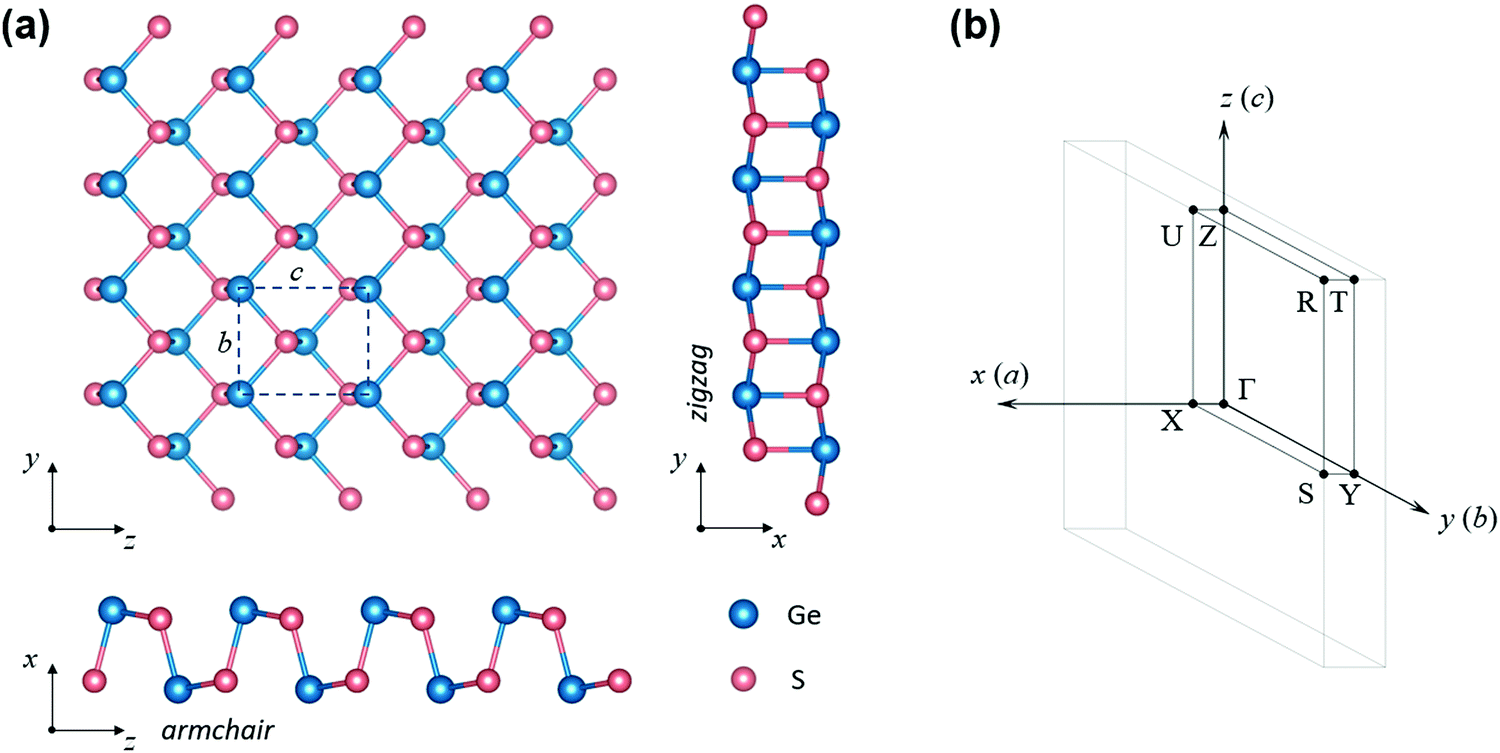 | ||
| Fig. 1 (a) Top and side views of the GeS crystal structure for a single layer. The armchair and zigzag directions are shown in relation to the crystal orientation and lattice parameters. (b) Brillouin zone and high-symmetry k-points. | ||
b. Experimental details
Samples placed inside a cryostat were investigated by optical absorption and photoreflectance (PR) measurements in the 20–300 K temperature range. The samples were illuminated with a halogen lamp and the reflected light was dispersed with a 0.55 m focal length single grating monochromator. The signal was detected with a Si photodiode and measured by the lock-in technique. For PR experiments, the reflectivity was modulated by a chopped (280 Hz) laser beam of a wavelength of 405 nm and power of 100 mW.GeS samples were grown by chemical vapor deposition at the HQ Graphene company. The purity of these samples is >99.995% as revealed from X-ray diffraction and energy-dispersive X-ray spectroscopy.51 For the PR method no special sample preparation is required. The measurements were performed on an as-grown bulk sample of ∼50 μm thickness and ∼2 mm in-plane dimensions. For polarization-resolved absorption measurements a smaller GeS flake was selected and thinned by mechanical exfoliation to a thickness of ∼8 μm, in order to obtain a higher intensity of transmitted light.
III. Results and discussion
a. GeS optical properties
Bulk GeS is a quasi-direct gap semiconductor with an indirect band gap of 1.56 eV at room temperature. This can be seen in Fig. 2, where PR and optical absorption spectra acquired at 20 K (Fig. 2(a)) and room temperature (Fig. 2(b)) are shown. Since PR is only sensitive to direct transitions, optical absorption is used to detect the indirect transition. Combining both techniques allows us to unambiguously discern the indirect nature of the GeS band gap, and establish the energies of the direct transitions. From the figure, the indirect gap, labeled E0, is slightly below the direct transitions revealed by the PR measurements, labeled E1 and E2. These results are in good agreement with previous reflectance,52 optical absorption24 and thermoreflectance26 measurements, which led to similar conclusions.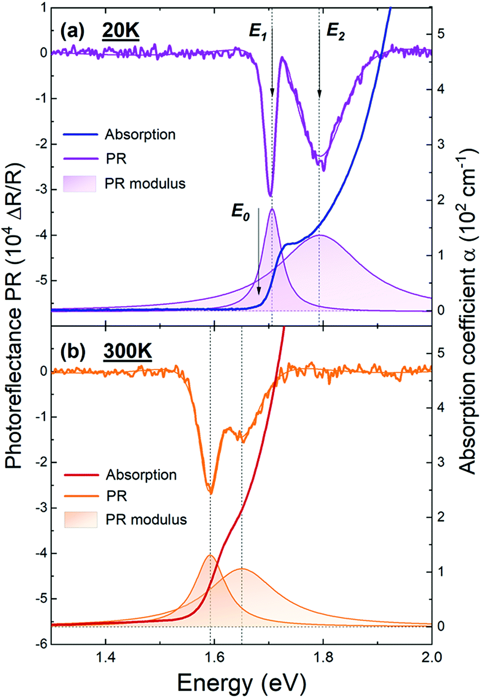 | ||
| Fig. 2 Photoreflectance and optical absorption spectra of GeS measured at 20 K (a) and ambient temperature (b). Eqn (1) fit to the PR spectra is also included, and the moduli of each of these two transitions are plotted at the bottom. | ||
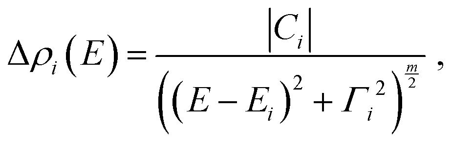
In order to extract the direct transition energies, the PR spectra in Fig. 2 are fitted (solid lines in the figure) with the Aspnes formula,53
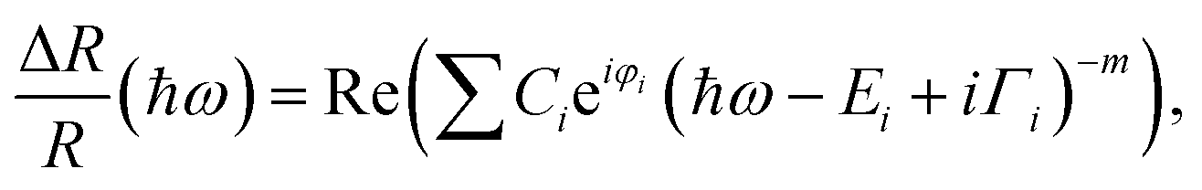 | (1) |
 | (2) |
The line shape of the absorption edge (see Fig. 2) consists of two distinctive features, corresponding to the indirect (E0) and direct transitions (E1). At low temperatures (Fig. 2(a)), these features form a plateau, which smooths out at ambient temperature (Fig. 2(b)) due to increased broadening of the transition energetic profile. Because of the overlapping of these two absorption features, it is not possible to determine the transition energies. However, owing to the strongly anisotropic character of these transitions, each one can be individually investigated by means of polarization-resolved measurements.22–24
b. Anisotropic properties of GeS
From the results presented in the previous section it can be seen that bulk GeS exhibits three optically active and closely-lying transitions, the fundamental indirect transition E0, and the two direct transitions E1 and E2. According to the literature, in GeS these transitions are highly anisotropic, but different interpretations were provided for their assignation. For instance, polarization-resolved optical absorption measurements revealed two features characteristic of two polarizations along the main in-plane crystallographic directions. In ref. 22 the authors identified the armchair and the zigzag polarized transitions as direct-allowed and direct-forbidden, respectively. On the contrary, in ref. 23 both transitions were considered as indirect forbidden. Recently, based on polarization-resolved absorption measurements combined with DFT calculations, the observed transitions were assigned away from the Γ point, along the Γ–Z and Γ–Y directions. The authors predict a partially dipole-allowed direct transition at lower energies (≈1.26 eV), at Γ.24 The optical properties of GeS were investigated also by means of polarization-resolved thermoreflectance.27 In the reported spectra two orthogonally polarized direct transitions were identified and assigned around the Γ point of the Brillouin zone.Because of the discrepancies present in the literature, a detailed study of the anisotropic properties of each transition has been conducted, by means of polarization-resolved PR and optical absorption measurements. The obtained results confirm that E1 and E2 are direct transitions, polarized along the armchair and zigzag directions, respectively, and E0 is the fundamental indirect transition. This can be seen in Fig. 3, where polarization-resolved PR (panel (a)) and absorption (panel (c)) spectra obtained at 20 K and at room temperature are presented. From the figure, it is clear that the lowest direct transition E1 is polarized in the armchair direction (0°) and the higher transition E2 is polarized along the zigzag direction (90°). The latter transition is absent in the absorption spectra due to the dominating contribution from energetically lower transitions. All the PR spectra are fitted with eqn (1), and the calculated modulus areas, Ai, are plotted as a function of polarization angle in a polar plot (Fig. 3(b)) at 20 K and room temperature. The angular dependence of Ai is fitted (solid lines) by using a modified Malus law,
f(φ) = f‖![[thin space (1/6-em)]](https://www.rsc.org/images/entities/char_2009.gif) cos2(φ − φ0) + f⊥sin2(φ − φ0), cos2(φ − φ0) + f⊥sin2(φ − φ0), | (3) |
 | (4) |
 | ||
| Fig. 3 (a) Polarization-resolved photoreflectance spectra acquired at 20 K (upper panel) and 300 K (lower panel), (b) polar plot of the oscillator strength A of transition E1 (green circles) and E2 (orange rhombus) and (c) polarization-resolved optical absorption spectra acquired at 20 K. | ||
From Fig. 3(b) it can be seen that transitions E1 and E2 are strongly polarized at low temperature (P = 97% and 87% respectively), but at ambient temperature the PR resonance attributed to the E2 transition exhibits a lower polarization degree of P = 68%. Such a decrease of the polarization degree can be associated with the contribution of the band-to-band component of the E1 transition, which is polarized along the armchair direction and is expected in similar spectral range to the E2 transition, due to the large exciton binding energy. In our analysis of the PR spectra, band-to-band transitions are neglected since they are significantly weaker than excitonic ones, but with the rise of temperature the relative intensity of band-to-band transitions increases, allowing observation of both mechanisms simultaneously.54
c. Temperature dependence of the direct and indirect transitions
The temperature-dependence of the optical properties of GeS has been scarcely investigated. Elkorashy23 reported temperature-dependent optical absorption measurements from 92 to 300 K and reported the temperature coefficients of the fundamental gap. Other studies only provide a comparison of measurements at low and at room temperature.22,26,27 In this section we present a comprehensive study of the temperature dependence of the indirect fundamental transition (E0) and the two direct transitions (E1 and E2). For this purpose we performed PR and absorption measurements in the temperature range from 20 to 300 K, with both polarized and unpolarized light.The PR spectra measured at different temperatures are shown in Fig. 4. The unpolarized spectra (Fig. 4(a)) exhibit two strong PR features, indicating the presence of two optically active direct transitions in this energy range. These transitions can be individually observed using light polarized along the in-plane crystallographic directions (Fig. 4(b)). The transition energies at each temperature were determined by fitting the spectra with eqn (1).
 | ||
| Fig. 4 (a) Unpolarized PR spectra and (b) PR spectra measured with polarization in the armchair and the zigzag directions, acquired at different temperatures. The smooth solid lines in panel (a) are the results of fitting the experimental data with eqn (1). | ||
Optical absorption spectra measured at different temperatures are shown in Fig. 5 with unpolarized (panel (a)), and linearly polarized (panels (b) and (c)) light. As can be seen in the unpolarized absorption, a characteristic step-like profile appears at low temperatures. This evidences the contribution of two transitions, labeled E0 and E1 in the figure. Since the E1 transition is strongly polarized in the armchair direction, measurements using zigzag polarization were performed to minimize the E1 signal and enable the investigation of the E0 transition. The spectra acquired for armchair polarization (Fig. 5(b)) exhibit a sharp rise of the absorption coefficient. The square root dependence of the absorption edge indicates that the E1 transition is direct. The measurements performed with zigzag polarized light (Fig. 5(c)) reveal a quadratic dependence of the absorption edge, confirming the indirect nature of transition E0. The energies of transitions E1 and E0 were extracted from the extrapolation of the α2 and α1/2 plots to zero, for the armchair and zigzag directions, respectively.
 | ||
| Fig. 5 (a) Unpolarized absorption spectra acquired at different temperatures. Features of the direct and indirect transitions are labeled. (b) Squared absorption coefficient versus energy acquired at different temperatures and with the armchair polarization direction. Direct energies are obtained from linear extrapolation. (c) Square root of the absorption coefficient versus energy acquired at different temperatures with the zigzag polarization direction. Indirect energies are obtained from linear extrapolation. | ||
Theoretical absorption coefficient spectra calculated from the real and imaginary part of the dielectric function are shown in Fig. S3 of the ESI.† The sharp rise of the armchair component occurs at an energy of ∼1.7 eV, which is in agreement with the experimentally observed direct transition E1. The calculations only reveal the absorption edge originating from direct transitions, and for this reason there is no contribution from the fundamental indirect band gap E0. Our calculations are in good agreement with those reported by Tan et al.24
The temperature dependences of all optical transition energies are plotted in Fig. 6 as obtained from PR (diamond symbols) and optical absorption (circles) measurements. The excellent agreement of the E1 energy versus temperature (green symbols) acquired from optical absorption and PR experiments polarized along the armchair direction ensures that both features are due to the same direct optical transition, and that the experimental uncertainty is smaller than 5 meV. As can be seen in the figure, GeS remains an indirect gap semiconductor throughout the whole temperature range, with a closely-lying direct transition. Finally, it is worth noting that while the transitions E0 and E1 exhibit a similar temperature dependence, the E2 transition features a significantly larger decrease of energy with temperature.
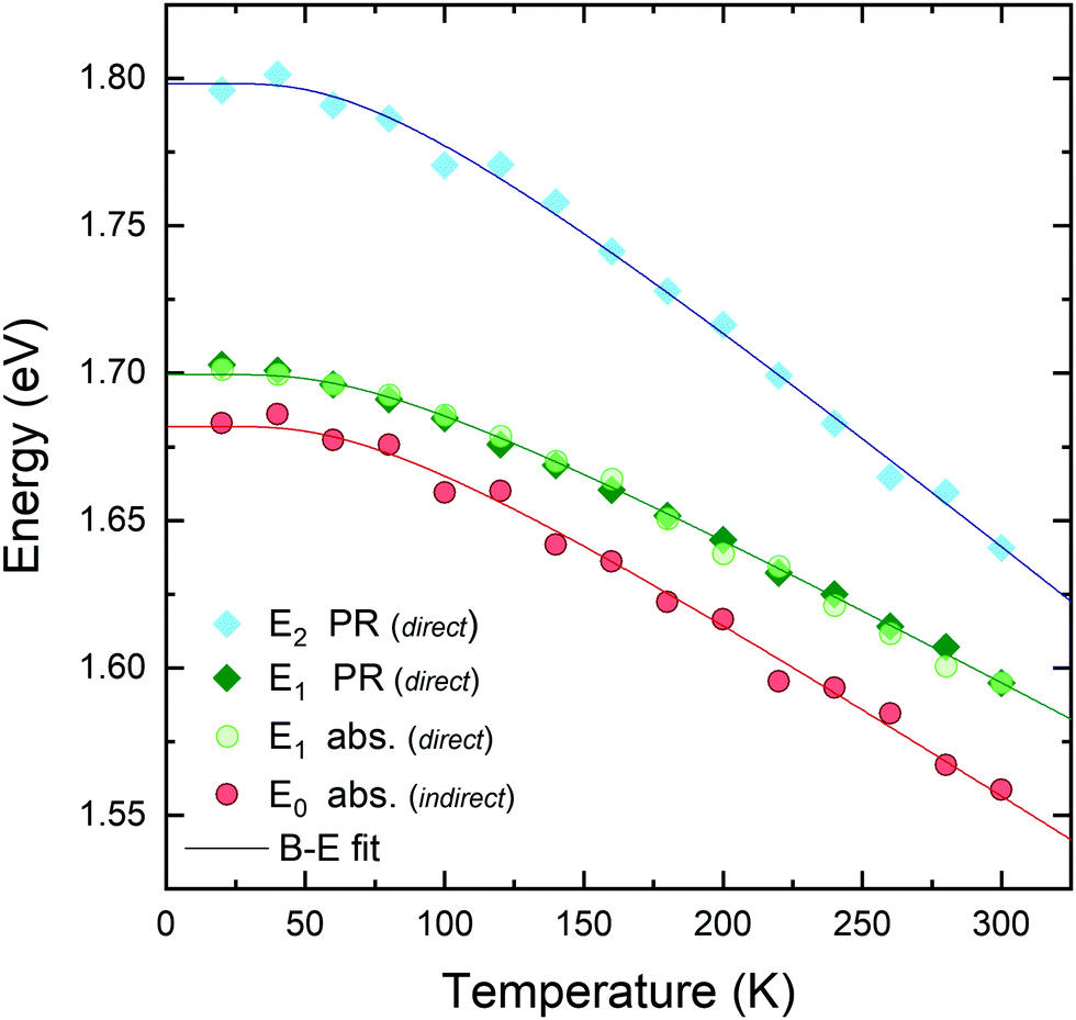 | ||
| Fig. 6 Temperature dependence of the energies of the direct and indirect transitions as measured by PR (diamond symbols) and optical absorption (circular symbols). A semi empirical B–E function (eqn (6)) has been fitted to each transition (solid lines). | ||
The temperature dependence of each optical transition has been approximated by both a commonly used semi-empirical Varshni relation and a relation derived from Bose–Einstein statistics. The Varshni formula is given by eqn (5)
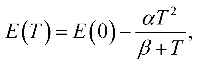 | (5) |
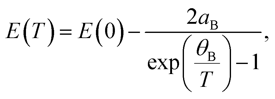 | (6) |
| Transition | Varshni | Bose–Einstein | ||||
|---|---|---|---|---|---|---|
| E(0) (eV) | α (10−4 eV K−1) | β (K) | E(0) (eV) | a B (meV) | θ B (K) | |
| E 0 | 1.689(3) | 6.73(93) | 160(65) | 1.685(1) | 51.3(1.2) | 178(30) |
| E 1 | 1.705(1) | 5.69(23) | 168(19) | 1.701(1) | 42.5(2.9) | 177(10) |
| E 2 | 1.802(3) | 11.10(20) | 312(107) | 1.797(1) | 93.3(1.4) | 235(25) |
From Table 1 it can be seen that the fundamental gap of GeS at 0 K is 1.685 eV (from the B–E fit), 16 meV lower than the first direct optical transition. While the aB and θB parameters extracted from the fit are almost identical between the E0 and E1 transitions, their values are significantly different for transition E2, which exhibits a stronger dependence on temperature. This suggests that E2 originates from a different region of the Brillouin zone, away from the Γ point.
d. Electronic band structure
Several DFT calculations of the GeS band structure have been reported so far. Previous calculations assigned the conduction band minimum (CBM) at the Γ point or in the Γ–Z direction33 and the valence band maximum (VBM) at Γ56 or at a k-point either in the Γ–Z33,35,57,58 or Γ–Y direction.31 These differences can be attributed to the particular choice of the exchange–correlation functional and lattice parameters. In order to properly describe the optoelectronic properties of GeS it is important to accurately evaluate the electronic band structure within the limitations of state-of-the-art DFT methods.The calculations presented here were performed with the use of the mBJ-TB09 potential and show a similar picture of the electronic band structure to that reported by Malone et al. from LDA-DFT and GW methods.29 As shown in Fig. 7, GeS is an indirect semiconductor whose CBM is located at the Δ point (i.e. at 2/3 of the Γ–Y path), and the VBM at different points along the Γ–Z direction. Such an arrangement of the band extrema in the high-symmetry directions is confirmed by calculations on a dense k-point grid in the Γ–Z–T–Y plane, as shown in Fig. S2 of the ESI.† It is worth noting that the upper valence band (shown in red in Fig. 7(b)) exhibits a very flat dispersion in the armchair direction (Γ–Z), and band crossing takes place in the zigzag direction (Γ–Y). These results are in perfect agreement with previously reported ARPES measurements, which report a VBM also at Γ–Z and close to Z.59,60 Interestingly, GeSe exhibits a similar electronic dispersion but with a reduced band gap due to the increased chalcogen size.61 Some of the possible direct and indirect transitions in the Z–Γ–Y region are schematically labelled in Fig. 7(b). Note that the band-nesting transitions are labeled as III and VI, and this kind of transition has been reported in other families of layered materials such as transition metal dichalcogenides.62,63 The electronic band structure calculated with the HSE06 hybrid functional is presented in Fig. S1 of the ESI.† This method yields similar energies of the valence band maxima in the armchair direction; however, it underestimates the energy of the maximum at the Δ point in the zigzag direction. The conduction band is upshifted by HSE06, with the most significant shift in the Δ–Y region, resulting in the CBM location at the Γ point.
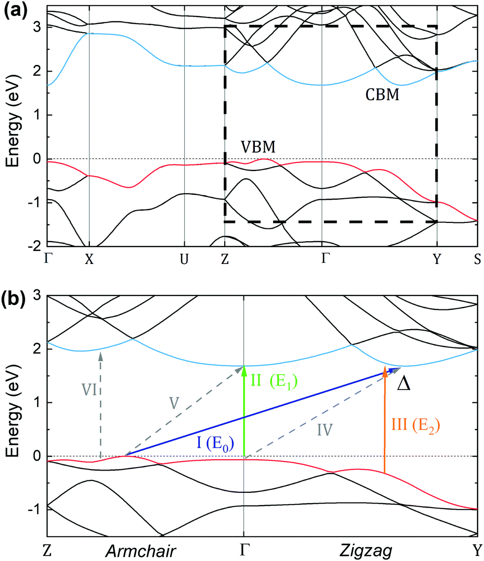 | ||
| Fig. 7 (a) Electronic band structure calculated with the mBJ-TB09 potential along the main high-symmetry directions in the Brillouin zone. (b) Electronic band structure along the Z–Γ–Y path, which corresponds to the armchair and the zigzag directions. The possible direct and indirect electronic transitions are labeled. | ||
An assignation for the E0, E1 and E2 optical transitions is provided in panel (b) of Fig. 7. The indirect transition E0 has been assigned to take place from the local maxima in the VB in the Γ–Z direction to the Δ point of the CB (shown as a blue arrow labeled I). The first sharp direct optical transition, E1, has been assigned to take place at Γ (shown as a green arrow labeled II). The second direct optical transition, E2, which exhibits a broad resonance profile (Γ2 ∼ 95 meV from the fit with eqn (1)) is assigned to the band nesting around Δ (shown as an orange arrow labelled III), where the conduction and valence bands are parallel. The assignation has been made taking into consideration three factors: (i) calculated and experimental energies, (ii) the polarization direction of each transition and (iii) the resonance broadening profile.
A comparison of theoretical and experimental values of these parameters is shown in Table 2. The transition energies calculated with the HSE06 functional are included in Table S1 of the ESI.† The agreement with experiment for transitions E0 and E1 is remarkable. Despite the fact that the standard DFT methods are known to underestimate the band gaps, the exchange–correlation functional employed here has been reported to be as accurate as hybrid functionals and GW methods.40 However, the calculated energy of transition E2 is significantly overestimated by ∼240 meV. The discrepancy between the experimental and the calculated energy (Eexp, and Ecalc, respectively) could be partially explained by the presence of a strongly bound exciton (Ecalc = Eexp + Eb) and an underestimation of the VB relative energy around Δ, which is a common feature in many DFT calculations for GeS.24,35 Due to the particular choice of computation method in our calculations excitonic effects are neglected. More work is desirable to establish the excitonic binding energies in GeS, both experimental ant theoretical.
| Transition | Assignation | Energy (eV) | Polarization, P (%) | ||
|---|---|---|---|---|---|
| Experiment | Calculation | Experiment | Calculation | ||
| a Optical absorption measurement. b Photoreflectance measurement. c mBJ-TB09 calculations. | |||||
| E 0 | Γ–Z → Δ | 1.685a | 1.607c | — | — |
| E 1 | Γ | 1.701b | 1.628c | Armchair, 97(2)% | Armchair, 100% |
| E 2 | Δ | 1.797b | 2.039c | Zigzag, 87(4)% | Zigzag, 100% |
In order to confirm the validity of the assignation proposed here, Table 2 shows also a comparison between the calculated and the experimental polarization directions for each transition. The calculated degree of polarization has been taken by using a formula analogous to eqn (4), P (%) = 100 × (|Pα|‖2 − |Pα|⊥2)/|Pα|‖2, where |Pα|‖2 and |Pα|⊥2 are the calculated matrix elements in the parallel and the perpendicular direction of the polarization direction, respectively. It is worth noting that the matrix elements calculated with the present methods have been shown to properly reproduce the relative PL intensity of TMDCs.64 Hence, these values are expected to describe well the anisotropic properties of GeS. From the table, excellent agreement is found between the theoretical and experimental polarization directions and polarization degree, which further supports the assignation proposed here.
IV. Conclusions
Summarizing, in the present work we showed that photoreflectance and optical absorption are complementary methods suitable for the investigation of the optical properties of van der Waals crystals. Optical absorption measurements revealed that the fundamental band gap of multilayer GeS is indirect with an energy of 1.685 eV and 1.56 eV at low and room temperature, respectively. Photoreflectance measurements allowed us to investigate two direct optical transitions, the first one at 1.70 eV (1.59 eV) at low (room) temperature, very close to the fundamental indirect gap, and the second one at 1.80 eV (1.64 eV) at low (room) temperature. The anisotropic properties of GeS were investigated by polarization-resolved measurements. It has been found that the direct optical transitions are highly anisotropic and can be individually selected by applying light linearly polarized along one of the main in-plane crystallographic directions. The temperature dependence of the fundamental band gap and energetically higher transitions was also studied, in order to determine the temperature coefficients of the transitions and support their identification. Finally, an assignation of each observed optical transition to a certain Brillouin zone point is provided, based on DFT calculations of the electronic band structure.Conflicts of interest
There are no conflicts to declare.Acknowledgements
This work was supported by the National Science Centre (NCN) Poland OPUS 11 no. 2016/21/B/ST3/00482. R. O. acknowledges the support from POLONEZ 3 no. 2016/23/P/ST3/04278. This project is carried out under POLONEZ program, which has received funding from the European Union's Horizon 2020 Research and Innovation program under the Marie Sklodowska-Curie grant agreement no. 665778. T. W. acknowledges support within the “Diamond Grant” (0026/DIA/2016/45) from the Polish Ministry of Science and Higher Education. DFT calculations were performed in the Wroclaw Centre for Networking and Supercomputing.References
- K. S. Novoselov, A. Mishchenko, A. Carvalho and A. H. C. Neto, Science, 2016, 353, aac9439 CrossRef CAS PubMed.
- A. V. Kolobov and J. Tominaga, Two-Dimensional Transition-Metal Dichalcogenides, Springer International Publishing, 2016 Search PubMed.
- M. Samadi, N. Sarikhani, M. Zirak, H. Zhang, H.-L. Zhang and A. Z. Moshfegh, Nanoscale Horiz., 2018, 3, 90–204 RSC.
- R. Oliva, T. Wozniak, F. Dybala, J. Kopaczek, P. Scharoch and R. Kudrawiec, Mater. Res. Lett., 2020, 8(2), 75–81 CrossRef CAS.
- D. Jariwala, V. K. Sangwan, L. J. Lauhon, T. J. Marks and M. C. Hersam, ACS Nano, 2014, 8, 1102–1120 CrossRef CAS PubMed.
- K. F. Mak and J. Shan, Nat. Photonics, 2016, 10, 216–226 CrossRef CAS.
- R. Ganatra and Q. Zhang, ACS Nano, 2014, 8, 4074–4099 CrossRef CAS PubMed.
- F. H. L. Koppens, T. Mueller, P. Avouris, A. C. Ferrari, M. S. Vitiello and M. Polini, Nat. Nanotechnol., 2014, 9, 780–793 CrossRef CAS PubMed.
- A. Castellanos-Gomez, J. Phys. Chem. Lett., 2015, 6, 4280–4291 CrossRef CAS PubMed.
- S. J. Zelewski and R. Kudrawiec, Sci. Rep., 2017, 7, 15365 CrossRef PubMed.
- A. Khandelwal, K. Mani, M. H. Karigerasi and I. Lahiri, Mater. Sci. Eng., B, 2017, 221, 17–34 CrossRef CAS.
- J. Qiao, X. Kong, Z.-X. Hu, F. Yang and W. Ji, Nat. Commun., 2014, 5, 4475 CrossRef CAS PubMed.
- M. Kim, H. Kim, S. Park, J. S. Kim, H. J. Choi, S. Im, H. Lee, T. Kim and Y. Yi, Angew. Chem., Int. Ed., 2019, 58, 3754–3758 CrossRef CAS PubMed.
- Q. Li, Q. Zhou, L. Shi, Q. Chen and J. Wang, J. Mater. Chem. A, 2019, 7, 4291–4312 RSC.
- L. C. Gomes, A. Carvalho and A. H. Castro Neto, Phys. Rev. B, 2016, 94, 054103 CrossRef.
- F. Li, X. Liu, Y. Wang and Y. Li, J. Mater. Chem. C, 2016, 4, 2155–2159 RSC.
- R. Ulaganathan, Y. Y. Lu, C. J. Kuo, S. Tamalampudi, R. Sankar, K. M. Boopathi, A. Anand, K. Yadav, R. Mathew, C. R. Liu, F. Chou and Y. T. Chen, Nanoscale, 2016, 8, 2284–2292 RSC.
- P. Zhao, H. Yang, J. Li, H. Jin, W. Wei, L. Yu, B. Huang and Y. Dai, J. Mater. Chem. A, 2017, 5, 24145–24152 RSC.
- C. Li, L. Huang, G. P. Snigdha, Y. Yu and L. Cao, ACS Nano, 2012, 6, 8868–8877 CrossRef CAS PubMed.
- M. Yang, S. Cao, Q. You, L.-B. Shi and P. Qian, Phys. E, 2020, 118, 113877 CrossRef CAS.
- A. M. Elkorashy, J. Phys.: Condens. Matter, 1990, 2, 6195–6205 CrossRef CAS.
- J. D. Wiley, A. Breitschwerdt and E. Schönherr, Solid State Commun., 1975, 17, 355–359 CrossRef CAS.
- A. M. Elkorashy, J. Phys. C: Solid State Phys., 1988, 21, 2595–2607 CrossRef CAS.
- D. Tan, H. E. Lim, F. Wang, N. B. Mohamed, S. Mouri, W. Zhang, Y. Miyauchi, M. Ohfuchi and K. Matsuda, Nano Res., 2017, 10, 546–555 CrossRef CAS.
- S. J. Zelewski and R. Kudrawiec, Sci. Rep., 2017, 7, 15365 CrossRef PubMed.
- C.-H. Ho and J.-X. Li, Adv. Opt. Mater., 2017, 5, 1600814 CrossRef.
- H.-C. Hsueh, J.-X. Li and C.-H. Ho, Adv. Opt. Mater., 2018, 6, 1701194 CrossRef.
- A. K. Singh and R. G. Hennig, Appl. Phys. Lett., 2014, 105, 042103 CrossRef.
- B. D. Malone and E. Kaxiras, Phys. Rev. B: Condens. Matter Mater. Phys., 2013, 87, 245312 CrossRef.
- L. C. Gomes, P. E. Trevisanutto, A. Carvalho, A. S. Rodin and A. H. Castro Neto, Phys. Rev. B, 2016, 94, 155428 CrossRef.
- B. R. Tuttle, S. M. Alhassan and S. T. Pantelides, Phys. Rev. B: Condens. Matter Mater. Phys., 2015, 92, 235405 CrossRef.
- L. Makinistian and E. A. Albanesi, Phys. Rev. B: Condens. Matter Mater. Phys., 2006, 74, 045206 CrossRef.
- L. Makinistian and E. A. Albanesi, Comput. Mater. Sci., 2011, 50, 2872–2879 CrossRef CAS.
- A. Rathor, V. Sharma, N. L. Heda, Y. Sharma and B. L. Ahuja, Radiat. Phys. Chem., 2008, 77, 391–400 CrossRef CAS.
- C. E. P. Villegas, A. R. Rocha and A. Marini, Phys. Rev. B, 2016, 94, 134306 CrossRef.
- G. Kresse and J. Furthmüller, Phys. Rev. B: Condens. Matter Mater. Phys., 1996, 54, 11169–11186 CrossRef CAS PubMed.
- G. Kresse and D. Joubert, Phys. Rev. B: Condens. Matter Mater. Phys., 1999, 59, 1758–1775 CrossRef CAS.
- J. P. Perdew, K. Burke and M. Ernzerhof, Phys. Rev. Lett., 1996, 77, 3865–3868 CrossRef CAS PubMed.
- A. Tkatchenko and M. Scheffler, Phys. Rev. Lett., 2009, 102, 073005 CrossRef PubMed.
- F. Tran and P. Blaha, Phys. Rev. Lett., 2009, 102, 226401 CrossRef PubMed.
- A. V. Krukau, O. A. Vydrov, A. F. Izmaylov and G. E. Scuseria, J. Chem. Phys., 2006, 125, 224106 CrossRef PubMed.
- H. Bilz and W. Kress, Phonon Dispersion Relations in Insulators, Springer-Verlag, Berlin Heidelberg, 1979 Search PubMed.
- O. Madelung, U. Rössler and M. Schulz, Germanium sulfide (GeS) phonon dispersion curves: Datasheet from Landolt-Börnstein – Group III Condensed Matter, Non-Tetrahedrally Bonded Elements and Binary Compounds I, Springer Materials, Springer-Verlag, Berlin Heidelberg, 1998 Search PubMed.
- H. Wiedemeier and P. A. Siemers, Z. Anorg. Allg. Chem., 1977, 431, 299–304 CrossRef CAS.
- J. Liu and S. T. Pantelides, Appl. Phys. Express, 2018, 11, 101301 CrossRef.
- W. H. Zachariasen, Phys. Rev., 1932, 40, 917–922 CrossRef CAS.
- G. Bissert and K.-F. Hesse, Acta Crystallogr., Sect. B: Struct. Crystallogr. Cryst. Chem., 1978, 34, 1322–1323 CrossRef.
- H. Wiedemeier and H. G. von Schnering, Z. Kristallogr., 1978, 148(3–4), 295–303 CrossRef CAS.
- R. W. G. Wyckoff, Cryst. Struct., 1963, 1, 85–237 Search PubMed.
- H. C. Hsueh, M. C. Warren, H. Vass, G. J. Ackland, S. J. Clark and J. Crain, Phys. Rev. B: Condens. Matter Mater. Phys., 1996, 53, 14806–14817 CrossRef CAS PubMed.
- GeS – Germanium sulfide, http://www.hqgraphene.com/GeS.php, (accessed July 6, 2020).
- Z. Li, Y. Yang, X. Wang, W. Shi, D.-J. Xue and J.-S. Hu, ACS Appl. Mater. Interfaces, 2019, 11, 24247–24253 CrossRef CAS PubMed.
- D. E. Aspnes, Surf. Sci., 1973, 37, 418–442 CrossRef CAS.
- M. Jarema, M. Gładysiewicz, Ł. Janicki, E. Zdanowicz, H. Turski, G. Muzioł, C. Skierbiszewski and R. Kudrawiec, J. Appl. Phys., 2020, 127, 035702 CrossRef CAS.
- L. Viña, S. Logothetidis and M. Cardona, Phys. Rev. B: Condens. Matter Mater. Phys., 1984, 30, 1979–1991 CrossRef.
- mp-2242, GeS (orthorhombic, Pnma, 62), https://materialsproject.org/materials/mp-2242, accessed November 27, 2019.
- Topological Materials Database, https://www.topologicalquantumchemistry.org/#/detail/1256, accessed November 27, 2019.
- L. C. Gomes and A. Carvalho, Phys. Rev. B: Condens. Matter Mater. Phys., 2015, 92, 085406 CrossRef.
- T. Grandke and L. Ley, Phys. Rev. B: Solid State, 1977, 16, 832–842 CrossRef CAS.
- V. Cháb and I. Bartoš, Phys. Status Solidi B, 1984, 121, 301–306 CrossRef.
- P. Mishra, H. Lohani, A. K. Kundu, R. Patel, G. K. Solanki, K. S. R. Menon and B. R. Sekhar, Semicond. Sci. Technol., 2015, 30, 075001 CrossRef.
- A. Carvalho, R. M. Ribeiro and A. H. Castro Neto, Phys. Rev. B: Condens. Matter Mater. Phys., 2013, 88, 115205 CrossRef.
- J. Kopaczek, M. P. Polak, P. Scharoch, K. Wu, B. Chen, S. Tongay and R. Kudrawiec, J. Appl. Phys., 2016, 119, 235705 CrossRef.
- T. Woźniak, P. E. Faria Junior, G. Seifert, A. Chaves and J. Kunstmann, Phys. Rev. B, 2020, 101, 235408 CrossRef.
Footnote |
| † Electronic supplementary information (ESI) available. See DOI: 10.1039/d0ma00146e |
| This journal is © The Royal Society of Chemistry 2020 |