DOI:
10.1039/D0MA00133C
(Paper)
Mater. Adv., 2020,
1, 658-665
Novel cost-effective acceptor:P3HT based organic solar cells exhibiting the highest ever reported industrial readiness factor†
Received
25th March 2020
, Accepted 1st June 2020
First published on 2nd June 2020
Abstract
Solution-based organic solar cells (OSCs) offer great potential prospects within low-cost electricity production. High-performance materials are traditionally low bandgap polymers requiring a multitude of synthetic steps, limiting the scalability of the materials. A very scalable polymer is poly(3-hexylthiophene) (P3HT) which has recently reached a power conversion efficiency (PCE) of 6.4% with a non-fullerene acceptor (NFA) O-IDTBR, herein we present four novel simplified NFA analogues to O-IDTBR for reducing the synthetic complexity. The best performing material combination reached an average efficiency of 5.39%, which led to an industrial readiness factor (i-FOM) of 0.26 which is more than a 30% increase compared to that for P3HT:O-IDTBR. Due to the promise of this material combination, upscaling to large area/ITO-free slot-die coating was conducted reaching an optimized PCE of 3.58%.
Introduction
For Organic solar cells (OSCs) to become economically viable, an important element to consider would be the production cost of the end product, i.e. electricity.1–4 This is mainly influenced by the cost of manufacture, power conversion efficiency (PCE), stability of the produced OSCs, and installation & maintenance (which will not be further evaluated, herein).2 The cost of manufacture has two main inputs: materials and processing. It is well-known that processing has to be conducted using techniques which are roll-to-roll compatible, as high-throughput is a necessity for reducing the processing cost, such techniques include slot-die coating, flexographic printing, screen printing, and to some extent thin-film vacuum deposition methods.5–9 In contrast, the cost of materials is a more debatable subject as a trade-off between cost of materials and the PCE of the produced OSCs are generally present. As record performances have only been achieved with highly complex molecules requiring a multitude of synthetic steps and limiting the overall yield, thereby increasing the material costs.10–13 Whereas P3HT is generally considered as the ideal donor (D) candidate for upscaling of OSCs with its simple synthesis, high hole mobility and high stability towards photo-oxidation. However, OSCs prepared with such simple low-cost materials as P3HT:PCBM commonly exhibit performance limitations, due to reduced photon absorption and large energy loss. These performance limitations have been overcome/improved by the implementation of non-fullerene acceptors (NFA)14,15 for devices paired with P3HT with VOC as high as 1.22 V16 and the extended absorption from ∼650 nm to ∼850 nm, leading to PCEs surpassing 6% when O-IDTBR17 and P3HT:SF(DPPB)418–21 were chosen. While somewhat simplified electron acceptors such as DFPCBR still reaches efficiencies of 5.25%.22 The highest efficiency achieved for P3HT based devices were reported recently by Xu et al. therein they presented an impressive device efficiency of up to 8.25%,23 however, this efficiency was only achieved through time-dependent ink modifications which definitely reduces the scalability of the ink system. Therefore, P3HT:O-IDTBR is still viewed as the most likely candidate for upscaling, even though the material system achieved an impressive PCE, later studies of the industrial figure of merit or industrial readiness (i-FOM) revealed that this material combination only scored 0.17 whereas 0.7 has been hypothesized as the required value.11 The i-FOM score is deducted from the relationship among device efficiency, stability, and synthetic complexity, revealing that simpler molecules with a reduced synthetic complexity could reduce the gap to the required i-FOM.
Herein we present two approaches for simplifying O-IDTBR to improve the obtained i-FOM value. Initially the benzothiadiazole was omitted to a avoid large number of synthetic steps, thereby reducing the synthetic complexity, moreover the electron donating core was substituted with less fused moieties to either adopt cost-effective starting materials or reduce their synthetic complexity24 even further and also to evaluate the effect of a core degree of fusing. The molecules presented herein are 4,9-dihydro-4,4,9,9-tetraoctyl-s-indaceno[1,2-b:5,6-b′]-dithiophene-dicarbaldehyde, 6-(5-formylthiophen-2-yl)-4,4-dioctyl-4H-indeno[1,2-b]thiophene-2-carbaldehyde, 5,5,10,10-tetraoctyl-5,10-dihydrothieno[2′,3′:3,4]cyclopenta[1,2-g]thieno[3,2-c]isochromene-2,8-dicarbaldehyde and 5,5′-(2,5-bis((2-ethylhexyl)oxy)-1,4-phenylene)bis(thiophene-2-carbaldehyde) flanked by 3-ethylrhodanine. The novel acceptors were initially characterized through NMR, MALDI-TOF, UV-Vis absorption and cyclic voltammetry. Their photovoltaic properties were firstly tested and optimized on small area spin-coated OSCs with P3HT as the donor polymer, after which the most promising material was transferred to large-area ITO-free slot-die coated OSCs.
Results
Physical properties
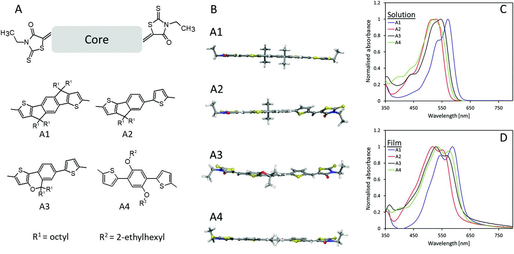
The chemical structure of the four novel electron acceptors (A1–A4) can be seen in Fig. 1A. The core molecules were synthesized according to literature25–28 after which Knoevenagel condensation between 3-ethylrhodanine and the dialdehyde functionalized core molecules were utilized to obtain the designed electron acceptors with a yield of 71.6%, 50.0%, 37.8%, and 60.1% for A1, A2, A3, and A4, respectively, further synthetic details can be seen in supporting information as well as molecular characterization (NMR Fig. S7 and MS Fig. S8, ESI†). The planarity of the prepared molecules was investigated through density functional theory (DFT) as seen in Fig. 1B, A1 was calculated to be essentially planar whereas both A2 and A3 appears less planar due to their non-fused core, e.g., for A2, the non-fused half of the molecule has a steric twist disrupting planarity and conjugation. The introduction of the ether bond into the fused part of the core molecule seems to create an additional steric twist within A3, resulting in a slight twisting of the fused part of the molecule. The calculations for A4 also displayed a dominantly planar molecule with just the slightest steric twisting. The increased planarity of A1 promotes an increase in conjugation length which in turn manifested in a red-shift of the absorption onset of 33 nm when compared to A2 (Fig. 1C and Table 1). Moreover, A1 also displays an enhanced J-aggregation strength (a relative enhancement in the primary absorption peak (first peak/plateau from the right in the absorption spectra) compared to the secondary absorption peak) which is associated with a reduced voltage loss.29–31 The film absorption (Fig. 1D) for all four materials exhibit red-shifts in their onset in a range of 29–42 nm, however, whereas A1 and A4 presents a λMax red-shift of 16 nm, A2 and A3 have slight blue-shifts in λMax of 13 and 17 nm, respectively, which implies a hinderance in π–π stacking likely due to the steric twists within the molecules.32,33 The absorbance spectra of blended films in a P3HT![[thin space (1/6-em)]](https://www.rsc.org/images/entities/char_2009.gif) :acceptor of 1:1 can be found in Fig. S1 ESI.†
:acceptor of 1:1 can be found in Fig. S1 ESI.†
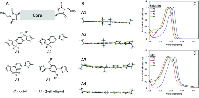 |
| | Fig. 1 (A) Chemical structures of A1, A2, A3, and A4; (B) optimized conformation of A1–A4 as calculated by DFT (B3LYP/6-31G*) with methyl groups replacing alkyl chains for clarity; (C) absorbance spectra of A1–A4 in chloroform solution; (D) absorbance spectra of A1–A4 films cast from chloroform solution. | |
Table 1 Optical and electrical characteristics of A1, A2, A3, and A4, namely absorption onset and maximum absorption for both CHCl3 solution and film, optical band gap (Eoptg), cyclic voltammetry determined band gap (EECg) and HOMO and LUMO levels positioning
|
|
Absorbance onset solution [nm] |
λ
Max solution [nm] |
Absorbance onset film [nm] |
λ
Max film [nm] |
E
optga film [eV] |
E
ECgb [eV] |
HOMO levelc [eV] |
LUMO leveld [eV] |
|
Estimated from the absorption onset in film: Eoptg = 1240/λonset.
E
ECg = EOX − ERED.
E
HOMO = −[EOX + (4.8 − EFC/FC+)].
E
LUMO = −[ERED + (4.8 − EFC/FC+)].
|
|
A1
|
608 |
1.74 |
637 |
587 |
1.95 |
2.06 |
−5.61 |
−3.55 |
|
A2
|
575 |
2.15 |
605 |
517 |
2.05 |
2.16 |
−5.57 |
−3.41 |
|
A3
|
592 |
2.00 |
627 |
529 |
1.98 |
1.99 |
−5.58 |
−3.59 |
|
A4
|
587 |
2.14 |
629 |
535 |
1.97 |
2.14 |
−5.71 |
−3.57 |
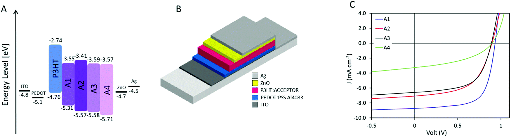
Cyclic voltammetry (CV) (ESI,† Fig. S2) of the thin films shows that A1–A3 have very similar highest occupied molecular orbital (HOMO) values around −5.6 eV whereas A4 possess a slightly lower one with −5.7 eV. As for the lowest unoccupied molecular orbital (LUMO), A1, A3, and A4 present very similar values in the range of −3.55 eV to −3.59 eV while A2 displaying a slightly higher one of −3.41 eV. The LUMO level of P3HT was measured as comparison to be −2.74 eV which would allow for sufficient energetic offset for optimum energy transfer between the donor and the acceptor(s). These acceptors are therefore all suitable for the preparation of OSCs pairing with P3HT as a donor.
Photovoltaic properties
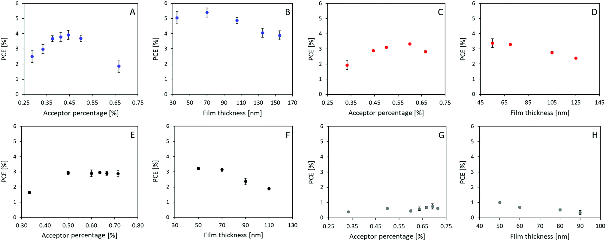
Solar cells were prepared with P3HT as the donor and A1–A4 as the acceptor, respectively, due to their matching energy levels (Fig. 2A) and low synthetic complexity. Devices were prepared in a normal geometry with a device stack of glass/ITO/PEDOT:PSS Al4083/Active layer/ZnO/Ag as displayed in Fig. 2B, similar to previously reported.34 All material combinations were optimized for annealing conditions (see ESI†), D:A ratio (Fig. 3A, C, E and G), and active layer film thickness (Fig. 3B, D, F and H), the specific photovoltaic characteristics can be found in ESI,† Fig. S3–S6 for A1–A4, respectively. The optimized J–V curve for the four material combinations can be found in Fig. 2C with the corresponding photovoltaic characteristics summarized in Table 2.
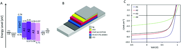 |
| | Fig. 2 (A) Energy level diagram for the prepared devices. (B) Schematic presentation of the prepared device structure, being normal architecture with a layer structure of glass/ITO/PEDOT:PSS Al4083/active layer/ZnO/Ag. (C) J–V characteristics of the hero device for the four novel acceptors. | |
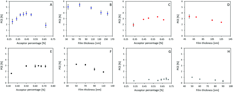 |
| | Fig. 3 Device fabrication parameter optimization, namely D:A ratio (acceptor percentage) and active layer thickness (film thickness) presented for P3HT:A1 in A and B, P3HT:A2 in C and D, P3HT:A3 in E and F, and P3HT:A4 in G and H. | |
Table 2 Tabular summarization of the photovoltaic characteristics of the optimized devices for each active layer combination, these averages are based on 8 devices with an area of 3.8 mm2
|
|
Ratio P3HT:acceptor |
Thickness [nm] |
V
OC [V] |
J
SC [mA cm−2] |
FF [%] |
PCE [%] |
|
A1
|
1:0.80 |
70 |
0.93 ± 0.01 |
8.69 ± 0.07 |
66.03 ± 0.7 |
5.39 ± 0.08 |
|
A2
|
1:1.50 |
55 |
0.89 ± 0.01 |
6.97 ± 0.10 |
53.90 ± 0.4 |
3.33 ± 0.03 |
|
A3
|
1:1.75 |
50 |
0.88 ± 0.01 |
6.49 ± 0.08 |
56.46 ± 3.4 |
3.21 ± 0.25 |
|
A4
|
1:2.25 |
50 |
0.83 ± 0.03 |
3.23 ± 0.04 |
37.20 ± 2.9 |
1.00 ± 0.12 |
The optimum D:A ratios were, with efficiencies of 3.92%, 3.33%, 2.96% and 0.75%, found to be 1:0.8, 1:1.5, 1:1.75, and 1:2.25 for P3HT:A1, A2, A3, and A4, respectively (as seen in Fig. 3A, C, E, and G). Interestingly, such optimized ratio switches unfavourably towards higher quantity of acceptor as the core becomes less fused and thereby obtains more degrees of freedom. Thinner films were generally found to be favourable, with only P3HT:A1 devices being improved upon increasing the film thickness from around 55 nm to 70 nm. The average optimized performances were found to be 5.39%, 3.37%, 3.21% and 1.00% for devices from P3HT:A1, A2, A3, and A4, respectively, as seen in Fig. 3B, D, F and H. The discovered limitations in film thicknesses could be ascribed to low charge carrier mobilities which inhere were determined through space charge limited current (SCLC) measurements of electron only (glass/ITO/ZnO/active layer/PFN/Ag) and hole only (glass/ITO/PEDOT:PSS Al4083/active layer/MoOx/Ag) devices, the obtained results are summarized in Table 3. As seen all active layers exhibit the values ranging from 7.82 × 10⁻⁵ cm2 (V c)−1 to 1.33 × 10⁻⁴ cm2 (V c)−1 for their reasonably similar hole mobilities, which correlates well with all devices utilizing P3HT as electron donor/hole transport material. The electron mobility is, however, significantly influenced by the choice of acceptor as it varies with more than one order of magnitude with P3HT:A1 reaching an electron mobility of 5.79 × 10⁻⁵ cm2 (V c)−1 whereas P3HT:A2, A3, and A4 exhibit their electron mobilities of ∼5 × 10⁻⁶ cm2 (V c)−1 clearly explaining the requirement for very thin films. It is evident that P3HT:A2–A4 films have a vastly imbalanced carrier transport with ratios of hole- to electron-mobility was found to be between 15 and 33. This suggests the main contributor to the reduced device FF could be imbalanced carrier transport. As for the observed variations in JSC, multiple factors may be contributing such as number of formed excitons, exciton dissociation, and free carrier extraction. The number of excitons would be directly correlated with the light harvesting under controlled film thickness which potentially could explain the differences among devices of P3HT:A1–A3 with varied Jsc of 6.49–8.69 mA cm−2 (as P3HT:A1 displays a red-shift in light absorbance and allows for increased film thickness (Fig. 1C and 3)). Exciton dissociation is generally influenced by energy level offsets and the phase-separation between the active layer materials. The energy level offsets are almost identical for the four material combinations presented herein and sufficient to ensure efficient dissociation (LUMO offsets significantly larger than the hypothesized 0.3 eV). It is therefore more likely that the JSC for these devices, especially P3HT:A4, is hindered by a non-optimal phase-separation allowing excitons to be recombined prior to dissociation. Free carrier extraction has been discussed above with P3HT:A2–A4 exhibiting a vastly imbalanced carrier mobility.
Table 3 Hole and electron mobility determined from SCLC experiments with hole and electron only devices with a structure of glass/ITO/PEDOT:PSS Al4083/active layer/MoOx/Ag and glass/ITO/ZnO/active layer/PFN/Ag, respectively. Charge carrier mobility balance was determined dividing the hole mobility with the electron mobility
| Acceptor |
Hole mobility (cm2 (V c)−1) |
Electron mobility (cm2 (V c)−1) |
Charge carrier mobility balance |
|
A1
|
1.04 × 10⁻⁴ ± 2.19 × 10⁻⁵ |
5.79 × 10⁻⁵ ± 8.80 × 10⁻⁶ |
1.8 |
|
A2
|
9.85 × 10⁻⁵ ± 2.07 × 10⁻⁵ |
6.51 × 10⁻⁶ ± 3.42 × 10⁻⁶ |
15.1 |
|
A3
|
7.82 × 10⁻⁵ ± 1.11 × 10⁻⁵ |
3.40 × 10⁻⁶ ± 7.23 × 10⁻⁷ |
23.0 |
|
A4
|
1.33 × 10⁻⁴ ± 3.43 × 10⁻⁵ |
4.01 × 10⁻⁶ ± 2.99 × 10⁻⁶ |
33.2 |
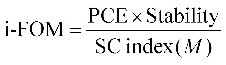
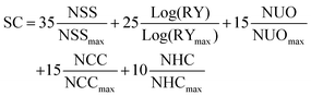
In order to do a proper quantification of the difference between A1 and O-IDTBR (and other novel materials), the previously published standardized i-FOM was applied for A1 and compared with that for O-IDTBR.11 The i-FOM is given by a relationship amongst device efficiency, stability after 200 h of light exposure, and synthetic complexity (SC) as presented in eqn (1).
| |  | (1) |
The equation for calculating i-FOM, based on the device PCE, device light stability after 200 h of light exposure, and the SC index (
M).
The SC of A1 was calculated as presented in eqn (2), it was described in literature based on the normalized number of synthetic steps (NSS), the normalized overall reciprocal yield (RY), the normalized number of operation units for purification (NUO), the normalized number of column chromatography for purification (NCC) and the normalized number of hazardous chemicals (NHC).10
| |  | (2) |
The equation for calculating SC with the values for NSS
max = 22, RY
max = 86.9, NUO
max = 39, NCC
max = 13, and NHC
max = 44 were taken from literature.
10
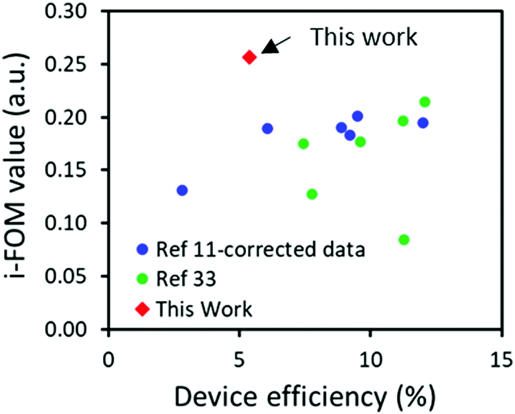
As presented in Table 4, a SC value of 36.7 was obtained for A1 which is a significant decrease of around 33% compared with that of 54.9 previously presented for O-IDTBR. This decrease in SC are to be expected as A1 is a form of simplification on O-IDTBR thereby reducing NSS, whilst the remaining synthetic steps are analogous due to the similarities of the molecules, therefore the increase in NHC from 16 in O-IDTBR to 29 in A1 caused wonderment. The NHC number presented for A1 herein was obtained on the basis of the guidelines put up in Po et al.,10 including purification solvents. The reduced SC value of A1 becomes even more pronounced compared to that of O-IDTBR when combined with P3HT, as the optimum D:A ratio for P3HT:A1 was found to be 1:0.8 compared to 1:1 for P3HT:O-IDTBR.17 Since P3HT has a SC score of 7.7, the combination of P3HT:A1 resulted in an SC index of 20.6 compared to 31.3 for P3HT:O-IDTBR. Such SC index combined with a PCE of 5.39 and an assumed stability of 0.98 (based on the device stability of P3HT:O-IDTBR) results in an i-FOM value of 0.26 which is not only significantly higher than that of 0.19 obtained for P3HT:O-IDTBR, but also the highest i-FOM value ever reported, as seen in Fig. 4.11,35 Such a high i-FOM value clearly demonstrates a strong potential of A1 as a stepping stone towards finding an industrial viable donor:acceptor pair for upscaling OSCs. The i-FOM may be increased even further by replacing the fused core with a non-fused core as demonstrated by Chen and coworkers.36
Table 4 Top section for calculations of the synthetic complexity (SC) on the basic of normalized number of synthetic steps (NSS), normalized reciprocal yield (RY), normalized number of operation units for purification (NUO), normalized number of column chromatography for purification (NCC) and normalized number of hazardous chemicals (NHC). Bottom section for calculation of the i-FOM based on SCacceptor, SCdonor, donor:acceptor ratio, PCE, and stability after 200 h of light exposure
| Synthetic complexity |
Norm_NSS |
Norm_RY |
Norm_NUO |
Norm_NCC |
Norm_NHC |
SC |
|
Assumed stability based on P3HT:O-IDTBR.
|
|
A1
|
0.32 |
0.28 |
0.41 |
0.38 |
0.66 |
36.7 |
| O-IDTBR |
0.5 |
0.70 |
0.62 |
0.46 |
0.36 |
54.9 |
| i-FOM calculation |
Ratio |
SCP3HT |
SC index (M) [%] |
PCE [%] |
Stability |
i-FOM |
|
A1
|
1:0.8 |
7.7 |
20.6 |
5.39 |
0.98a |
0.26 |
| O-IDTBR |
1:1 |
7.7 |
31.3 |
6.05 |
0.98 |
0.19 |
 |
| | Fig. 4 A comparison of the industrial readiness factors (i-FOM) against previously published ones as a function of device efficiency. | |
Upscaling of P3HT:A1 to large area slot-die coated ITO-free organic solar cells.
As the active layer material combination of P3HT:A1 with an i-FOM value of 0.26 displays a great potential for being at least a stepping stone towards industrial relevance. Large area ITO-free OSCs with an area of 0.88 cm2 were fabricated and optimized through slot-die coating (except for the Ag and Al electrodes which were flexographically printed and thermally evaporated, respectively) with the layer stack of PET/Ag/PEDOT:PSS/P3HT:A1/ZnO/Al in normal geometry as seen in Fig. 5A. In an attempt to make the transfer from small-area spin-coated device to the large-area coated and printed devices less complicated, direct transfer of the D:A ratio of 1:0.8 and annealing conditions 140 °C for 4 min was adapted. An active layer thickness of 70 nm was deemed too thin in comparison with the previously reported thinnest one in normal geometry large-area OSCs of 150 nm8. And chloroform, being a very low evaporation temperature solvent, is generally not viewed as an optimal solvent for large-area OSCs fabrication, therefore a solvent mixture of chlorobenzene and chloroform (CB:CF) 90:10 was chosen.37 As an initial investigation, the type of additive was determined by preparing devices with 5% additive of either chloronaphthalene (CN), 1,2,3,4-tetrahydronaphthalene (THN), 4-bromoanisole (BrA), 1,8-diiodooctane (DIO), or ortho-dichlorobenzene (o-DCB). THN, BrA, and o-DCB have previously been utilized with P3HT:O-IDTBR with great success.38,39 However, from the obtained results herein (Fig. 5B), it can be seen that only DIO or o-DCB with PCE of 1.1% enhances the device efficiency above the CB:CF base solvent mixture. As the material combination have proven to be highly thickness dependent, a series of device with active layer thicknesses ranging from 70–220 nm were prepared. As illustrated in Fig. 5C, 100 nm is found to be the optimized active layer thickness with slight decrease in efficiency of approximately 10% for the a bit thinner one (70 nm), and with a plateau of 70% of the optimum for devices with active layer above 150 nm. The underlying reasons for the relatively low device performance were investigated through a thermal annealing test as can be seen in Table S4 in the ESI,† 140 °C appears to be too high a temperature as the device efficiency only decreases with extended annealing time. Therefore, the annealing temperature was lowered to 120 °C for both pre- and post-annealing of the prepared devices for the following experiments. The ink composition was optimized firstly through varying the o-DCB concentration, giving a peak efficiency of 3.58% at 20% o-DCB with low molecular weight P3HT (20 kDa). While high molecular weight P3HT (60 kDa) only allows a hero efficiency of 2.68% as seen in Fig. 5D. Secondly through variation of chloroform content in the inks as displayed in Fig. 5E, a chloroform concentration of 20% appears to be optimum with a slight device efficiency increase from 10% to 20% before decreasing again at 30% chloroform in the ink mixture. From Fig. 5E it is also clearly evident that devices with ethanol based ZnO have superior performance over acetone based ones, likely do to with solubilities as A1 exhibits slight soluble in acetone, leading to a depletion of A1 in the top part of the active layer and a mixed ETL due to the deposition of acetone based ZnO.
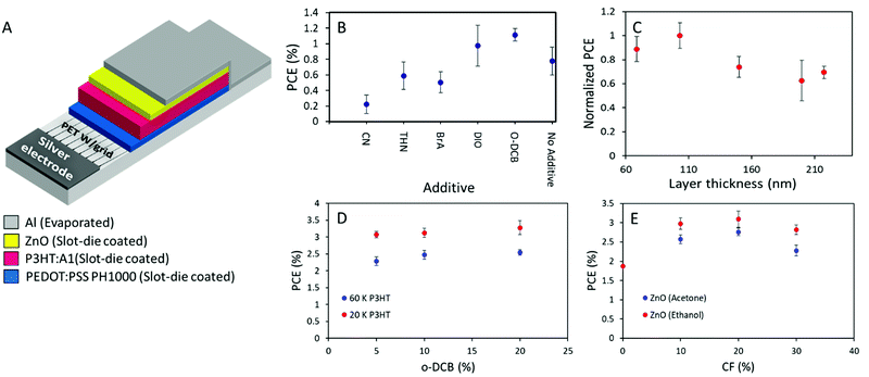 |
| | Fig. 5 (A) Schematic presentation of the printed layer-stack for normal geometry flexible OSCs. (B) Device efficiencies as a function of additive with a concentration of 5% (chloronaphthalene (CN), 1,2,3,4-tetrahydronaphthalene (THN), 4-bromoanisole (BrA), 1,8-diiodooctane (DIO), ortho-dichlorobenzene (o-DCB)). (C) Normalized device efficiency as a function of active layer thickness. (D) PCE of prepared devices with two different P3HT with Mw of 20 kDa and 60 kDa, respectively, as a function of o-DCB concentration. (E) Device PCEs as a function of chloroform concentration with ZnO deposited from either acetone or ethanol. | |
In recent literatures, a multitude of minor deposition variations have proven highly efficient for the sake of enhancing the efficiency of slot-die coated OSCs devices. Initially, Na et al. presented an impressive efficiency optimization from approximately 2.5% to around 8% through controlling the substrate and slot-die coating-head temperatures during active layer deposition.40 Implementing this approach did, however, not have a positive influence on our prepared devices, as we observed a decrease in device performance from around 2.5% to 1.2% with increased substrate temperature from 60 to 80 °C, and a further temperature increase to 100 °C did not appear to change the performance further, as seen in Fig. 6A. Meng et al. published another approach, in which they significantly decreased the concentration of the ink, illustrating that the obtained morphology can much better emulate spin-coating with a PCE around 9.5%.41 Meanwhile this approach did not result in improved device efficiencies for the system presented herein, as seen in Fig. 6B, no differences were observed in the device efficiency when diluting the active layer ink from 12.6 mg mL−1 to 6.3 mg mL−1.
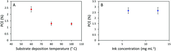 |
| | Fig. 6 (A) Device PCE development as a function of substrate deposition temperature. (B) Device efficiency as a function of ink concentration with concentrations of 6.3 mg mL−1 and 12.6 mg mL−1. | |
Conclusion
In this work, we present four novel small molecule non-fullerene acceptors with four different core-molecules (4,9-dihydro-4,4,9,9-tetraoctyl-s-indaceno[1,2-b:5,6-b′]-dithiophene-dicarbaldehyde, 6-(5-formylthiophen-2-yl)-4,4-dioctyl-4H-indeno[1,2-b]thiophene-2-carbaldehyde, 5,5,10,10-tetraoctyl-5,10-dihydrothieno[2′,3′:3,4]cyclopenta[1,2-g]thieno[3,2-c]isochromene-2,8-dicarbaldehyde and 5,5′-(2,5-bis((2-ethylhexyl)oxy)-1,4-phenylene)bis(thiophene-2-carbaldehyde)) flanked by 3-ethylrhodanine. These molecules were designed as synthetically simplified alternatives to O-IDTBR as acceptors for the best cost-effective donor polymer P3HT. As a consequence of the simplified structure of A1–A4, their optical absorbance has a greater overlap with P3HT than previously reported O-IDTBR. The optical band gaps of the acceptor presented herein are between 1.95 eV and 2.05 eV, due to their difference in core rigidity allowing A2 to twist thereby disrupting the molecular packing. A1–A4 exhibited HOMO-levels between −5.71 eV and −5.57 eV and LUMO-levels between −3.41 eV and −3.59 eV, which are suitable for pairing with P3HT. The optimized P3HT:A1–A4 devices yielded efficiencies of 5.39, 3.33, 3.21, and 1.00% for A1, A2, A3, and A4, respectively, with optimum ratios pushed towards higher amount of acceptor with less fused cores. The simplified structure of A1 combined with the device efficiency of 5.39% resulted in an i-FOM (industrial readiness measure) value of 0.26 which is more than a 30% increase over that of O-IDTBR and the highest ever reported i-FOM value. The P3HT:A1 combination was upscaled to large-area ITO-free slot-die coated OSCs, reaching an optimized efficiency up to 3.58%.
Conflicts of interest
There are no conflicts to declare.
Acknowledgements
TRA and ATW contributed equally to this work. TRA would like to greatly acknowledge the financial support from National Natural Science Foundation of China (No. 51850410580). QT thanks support from China Scholarship Council (CSC), Grants from Natural Science Foundation of Hunan Province (Grant No. 2015JJ2042, 2018JJ3098) and the Scientific Research Fund of Hunan Provincial Education Department (No. 18A344). Support from Sino-Danish Center for Education and Research is fully acknowledged by DY.
References
- S. E. Shaheen, D. S. Ginley and G. E. Jabbour, MRS Bull., 2005, 30, 10–19 CrossRef CAS.
- C. J. Mulligan, C. Bilen, X. Zhou, W. J. Belcher and P. C. Dastoor, Sol. Energy Mater. Sol. Cells, 2015, 133, 26–31 CrossRef CAS.
- C. J. Brabec, Sol. Energy Mater. Sol. Cells, 2004, 83, 273–292 CrossRef CAS.
- B. Azzopardi, C. J. M. Emmott, A. Urbina, F. C. Krebs, J. Mutale and J. Nelson, Energy Environ. Sci., 2011, 4, 3741 RSC.
- F. C. Krebs, Sol. Energy Mater. Sol. Cells, 2009, 93, 394–412 CrossRef CAS.
- F. C. Krebs, Sol. Energy Mater. Sol. Cells, 2009, 93, 465–475 CrossRef CAS.
- F. C. Krebs, S. A. Gevorgyan and J. Alstrup, J. Mater. Chem., 2009, 19, 5442–5451 RSC.
- T. R. Andersen, F. Almyahi, N. A. Cooling, D. Elkington, L. Wiggins, A. Fahy, K. Feron, B. Vaughan, M. J. Griffith, A. J. Mozer, C. Sae-kung, G. G. Wallace, W. J. Belcher and P. C. Dastoor, J. Mater. Chem. A, 2016, 4, 15986–15996 RSC.
- T. R. Andersen, N. A. Cooling, F. Almyahi, A. S. Hart, N. C. Nicolaidis, K. Feron, M. Noori, B. Vaughan, M. J. Griffith, W. J. Belcher and P. C. Dastoor, Sol. Energy Mater. Sol. Cells, 2016, 149, 103–109 CrossRef CAS.
- R. Po, G. Bianchi, C. Carbonera and A. Pellegrino, Macromolecules, 2015, 48, 453–461 CrossRef CAS.
- N. Li, I. McCulloch and C. J. Brabec, Energy Environ. Sci., 2018, 11, 1355–1361 RSC.
- J. Min, Y. N. Luponosov, C. Cui, B. Kan, H. Chen, X. Wan, Y. Chen, S. A. Ponomarenko, Y. Li and C. J. Brabec, Adv. Energy Mater., 2017, 7, 1700465 CrossRef.
- J. Yuan, Y. Zhang, L. Zhou, G. Zhang, H.-L. Yip, T.-K. Lau, X. Lu, C. Zhu, H. Peng, P. A. Johnson, M. Leclerc, Y. Cao, J. Ulanski, Y. Li and Y. Zou, Joule, 2019, 3, 1140–1151 CrossRef CAS.
- Y. Lin, J. Wang, Z.-G. Zhang, H. Bai, Y. Li, D. Zhu and X. Zhan, Adv. Mater., 2015, 27, 1170–1174 CrossRef CAS PubMed.
- S. Li, L. Ye, W. Zhao, X. Liu, J. Zhu, H. Ade and J. Hou, Adv. Mater., 2017, 29, 1704051 CrossRef PubMed.
- B. Xiao, A. Tang, J. Yang, Z. Wei and E. Zhou, ACS Macro Lett., 2017, 6, 410–414 CrossRef CAS.
- S. Holliday, R. S. Ashraf, A. Wadsworth, D. Baran, S. A. Yousaf, C. B. Nielsen, C.-H. Tan, S. D. Dimitrov, Z. Shang, N. Gasparini, M. Alamoudi, F. Laquai, C. J. Brabec, A. Salleo, J. R. Durrant and I. McCulloch, Nat. Commun., 2016, 7, 11585 CrossRef CAS PubMed.
- S. Li, W. Liu, M. Shi, J. Mai, T.-K. Lau, J. Wan, X. Lu, C.-Z. Li and H. Chen, Energy Environ. Sci., 2016, 9, 604–610 RSC.
- W. Liu, S. Li, J. Huang, S. Yang, J. Chen, L. Zuo, M. Shi, X. Zhan, C.-Z. Li and H. Chen, Adv. Mater., 2016, 28, 9729–9734 CrossRef CAS PubMed.
- J. I. Khan, R. S. Ashraf, M. A. Alamoudi, M. N. Nabi, H. N. Mohammed, A. Wadsworth, Y. Firdaus, W. Zhang, T. D. Anthopoulos, I. McCulloch and F. Laquai, Sol. RRL, 2019, 3, 1900023 CrossRef.
- A. Wadsworth, Z. Hamid, M. Bidwell, R. S. Ashraf, J. I. Khan, D. H. Anjum, C. Cendra, J. Yan, E. Rezasoltani, A. A. Y. Guilbert, M. Azzouzi, N. Gasparini, J. H. Bannock, D. Baran, H. Wu, J. C. de Mello, C. J. Brabec, A. Salleo, J. Nelson, F. Laquai and I. McCulloch, Adv. Energy Mater., 2018, 8, 1801001 CrossRef.
- N. Wang, W. Yang, S. Li, M. Shi, T.-K. Lau, X. Lu, R. Shikler, C.-Z. Li and H. Chen, Chin. Chem. Lett., 2019, 30, 1277–1281 CrossRef CAS.
- X. Xu, G. Zhang, L. Yu, R. Li and Q. Peng, Adv. Mater., 2019, 31, 1906045 CrossRef CAS PubMed.
- S. Li, L. Zhan, F. Liu, J. Ren, M. Shi, C.-Z. Li, T. P. Russell and H. Chen, Adv. Mater., 2018, 30, 1705208 CrossRef PubMed.
-
Q. Tao and D. Yu, to be published.
- W. Zhang, J. Smith, S. E. Watkins, R. Gysel, M. McGehee, A. Salleo, J. Kirkpatrick, S. Ashraf, T. Anthopoulos, M. Heeney and I. McCulloch, J. Am. Chem. Soc., 2010, 132, 11437–11439 CrossRef CAS PubMed.
- H. Chen, A. Wadsworth, C. Ma, A. Nanni, W. Zhang, M. Nikolka, A. M. T. Luci, L. M. A. Perdigão, K. J. Thorley, C. Cendra, B. Larson, G. Rumbles, T. D. Anthopoulos, A. Salleo, G. Costantini, H. Sirringhaus and I. McCulloch, J. Am. Chem. Soc., 2019, 141, 18806–18813 CrossRef CAS PubMed.
- L. Cai, T. Moehl, S.-J. Moon, J.-D. Decoppet, R. Humphry-Baker, Z. Xue, L. Bin, S. M. Zakeeruddin and M. Grätzel, Org. Lett., 2014, 16, 106–109 CrossRef CAS PubMed.
- G. Zeng, J. Ouyang, Y. Xin, X. Zhao and X. Yang, J. Mater. Chem. C, 2018, 6, 13211–13217 RSC.
- S. Li, L. Zhan, T.-K. Lau, Z.-P. Yu, W. Yang, T. R. Andersen, Z. Fu, C.-Z. Li, X. Lu, M. Shi and H. Chen, Small Methods, 2019, 3, 1900531 CrossRef CAS.
- S. Li, L. Zhan, C. Sun, H. Zhu, G. Zhou, W. Yang, M. Shi, C.-Z. Li, J. Hou, Y. Li and H. Chen, J. Am. Chem. Soc., 2019, 141, 3073–3082 CrossRef CAS PubMed.
- S. Li, L. Zhan, W. Zhao, S. Zhang, B. Ali, Z. Fu, T.-K. Lau, X. Lu, M. Shi, C.-Z. Li, J. Hou and H. Chen, J. Mater. Chem. A, 2018, 6, 12132–12141 RSC.
- N. Wang, L. Zhan, S. Li, M. Shi, T.-K. Lau, X. Lu, R. Shikler, C.-Z. Li and H. Chen, Mater. Chem. Front., 2018, 2, 2006–2012 RSC.
- L. Zhan, S. Li, T.-K. Lau, Y. Cui, X. Lu, M. Shi, C.-Z. Li, H. Li, J. Hou and H. Chen, Energy Environ. Sci., 2020, 13, 635–645 RSC.
- X. Du, T. Heumueller, W. Gruber, A. Classen, T. Unruh, N. Li and C. J. Brabec, Joule, 2019, 3, 215–226 CrossRef CAS.
- Z.-P. Yu, Z.-X. Liu, F.-X. Chen, R. Qin, T.-K. Lau, J.-L. Yin, X. Kong, X. Lu, M. Shi, C.-Z. Li and H. Chen, Nat. Commun., 2019, 10, 1–9 CrossRef PubMed.
- T. R. Andersen, H. F. Dam, B. Andreasen, M. Hösel, M. V. Madsen, S. A. Gevorgyan, R. R. Søndergaard, M. Jørgensen and F. C. Krebs, Sol. Energy Mater. Sol. Cells, 2014, 120, 735–743 CrossRef CAS.
- S. Strohm, F. Machui, S. Langner, P. Kubis, N. Gasparini, M. Salvador, I. McCulloch, H.-J. Egelhaaf and C. J. Brabec, Energy Environ. Sci., 2018, 11, 2225–2234 RSC.
- E. Pascual-San-José, X. Rodríguez-Martínez, R. Adel-Abdelaleim, M. Stella, E. Martínez-Ferrero and M. Campoy-Quiles, J. Mater. Chem. A, 2019, 7, 20369–20382 RSC.
- S.-I. Na, Y.-H. Seo, Y.-C. Nah, S.-S. Kim, H. Heo, J.-E. Kim, N. Rolston, R. H. Dauskardt, M. Gao, Y. Lee and D. Vak, Adv. Funct. Mater., 2019, 29, 1805825 CrossRef.
- X. Meng, L. Zhang, Y. Xie, X. Hu, Z. Xing, Z. Huang, C. Liu, L. Tan, W. Zhou, Y. Sun, W. Ma and Y. Chen, Adv. Mater., 2019, 31, 1903649 CrossRef CAS PubMed.
Footnote |
| † Electronic supplementary information (ESI) available. See DOI: 10.1039/d0ma00133c |
|
| This journal is © The Royal Society of Chemistry 2020 |
Click here to see how this site uses Cookies. View our privacy policy here. 
 Open Access Article
 This Open Access Article is licensed under a
  *a,
Anne Therese
Weyhe
b,
Qiang
Tao
bc,
Feng
Zhao
a,
Ran
Qin
*a,
Anne Therese
Weyhe
b,
Qiang
Tao
bc,
Feng
Zhao
a,
Ran
Qin