
 Open Access Article
 This Open Access Article is licensed under a
 Creative Commons Attribution 3.0 Unported Licence
Inkjet printed mesoscopic perovskite solar cells with custom design capability†
Anand
Verma
 a,
David
Martineau
b,
Sina
Abdolhosseinzadeh
ac,
Jakob
Heier
a and
Frank
Nüesch
*ac
a,
David
Martineau
b,
Sina
Abdolhosseinzadeh
ac,
Jakob
Heier
a and
Frank
Nüesch
*ac
aLaboratory for Functional Polymers, Swiss Federal Laboratories for Materials Science and Technology (Empa), Überlandstrasse 129, CH-8600 Dübendorf, Switzerland. E-mail: frank.nueesch@empa.ch
bSolaronix, SA, Rue de l'Ouriette 129, CH-1170 Aubonne, Switzerland
cInstitut des matériaux, École Polytechnique Fédérale de Lausanne (EPFL), CH-1015 Lausanne, Switzerland
First published on 24th April 2020
Abstract
Customizable solar cells are required for aesthetic indoor and outdoor photovoltaic deployment as well as for the freedom of design of small and portable power supplies. We demonstrate that drop on demand inkjet printing can be used for the fabrication of monolithic mesoscopic carbon-based perovskite solar cells by printing all of the oxide layers in the stack as well as the organo-metal halide absorber. Printable inks using environmentally friendly solvents and jetting parameters were developed in order to achieve homogenous and continuous functional layers of the photovoltaic stack. Inkjet printed cells are compared to those obtained from the standard screen-printing route. As a proof of principle, photovoltaic cells with an area of 1.5 cm2 and a performance of 9.1% were realized by inkjet printing, which opens up intriguing application possibilities.
Introduction
Economy of scale has led to an amazing deployment of crystalline silicon solar cell technology in the past decades.1 While this development has established industrial manufacture of square or rectangular module shapes for convenient coverage of large areas, few technologies have addressed the production of customized shapes for photon to electrical energy conversion.2–4 Crystalline solar cells with particular shapes5 improving the aesthetics or even dummies are typical approaches used in building integration.6 Such approaches, however are always limited by processing constraints and full freedom of design can only be reached if photovoltaic cells can be fabricated by printing techniques.2 Digital stencil-less techniques such as drop-on-demand (DOD) inkjet printing are particularly compelling for this purpose. In addition, they offer straightforward industrialization capability.7,8Inkjet printing has quite widely been used in photovoltaic device fabrication, e.g. for depositing silver lines or antireflective structures on crystalline silicon wafers.9 Contrary to wafer technologies, thin film photovoltaic technologies allow to inkjet the active materials of the solar cell stack. For example, inkjet printed chalcopyrite10 and kesterite11 absorbers have demonstrated promising device efficiencies. Among the possible solar cell technologies fulfilling the requirements for inkjet printing, organic solar cells have been most widely studied and fully inkjet printed devices have indeed been achieved.12–14 However, the rather modest device efficiencies of 3–4% have dampened enthusiasm along this direction. The same is true for dye-sensitized solar cells (DSSCs). In the latter case, inkjet printing allowed to finely dose the appropriate volume of liquid electrolyte into the mesoporous oxide layer.15 Another study reported on staining the TiO2 photoelectrode by inkjet printing.16 It is more challenging to inkjet print nanoparticle inks due to nozzle clogging and it is all the more remarkable that deposition of the mesoporous TiO2 layer has been achieved by DOD technique.17 Despite these substantial achievements, inkjet printing of DSSCs has not received much attention, probably, because device efficiency stayed below 5–6%. Renewed interest in inkjet printing has been spurred by the soaring performance of the young lead-halide perovskite solar cell (PSC) technology.18 Advantageously, PSC stacks can be printed at low temperature, much the same way as for organic solar cells. One critical component is the absorber layer itself, which ideally consists of a continuous, large grained crystalline layer in planar architectures. Few works reported on inkjet-printed CH3NH3PbI3 (MAPI) layers directly on planar compact TiO2 (c-TiO2) coated conductive glass substrates and employed a vacuum assisted post-treatment to achieve uniform crystalline films.19,20 Other works used a thin mesoporous TiO2 (m-TiO2) electron extraction layer, on top of which lead-iodide was first inkjet printed and subsequently converted to the perovskite by using inter-diffusion of methyl-ammonium iodide.21 Interestingly, it was noted that the mesoscopic layer provided a perfect wetting layer for lead-iodide, pinning the liquid at the boundary of the oxide layer. Alternatively, it was shown that a blend of nanocarbon and methyl-ammonium iodide can be inkjet printed onto the lead-iodide film. By means of a diffusion process, the latter transforms into the active perovskite absorber with overlaying carbon electrode.22 Another work has achieved both the sequential deposition of thin m-TiO2 and the perovskite layer to achieve an average efficiency of 12.2% on small laboratory cell areas.23 Among the various perovskite device architectures, the so-called triple layer mesoporous metal-oxide monolithic architecture using a porous carbon back contact (MPSC) presents considerable advantages for inkjet printing the active perovskite absorber (Fig. 1).24,25 In those types of cells, a porous scaffold consisting of a mesoporous TiO2 layer (m-TiO2), a mesoporous ZrO2 (m-ZrO2) layer followed by a porous carbon layer presents an excellent texture for infiltrating the lead-halide salt ink droplets. Furthermore, the robust and rather thick cell architecture is defect tolerant and promises straightforward large area scale-up. The extremely thick hydrophobic carbon layer prevents water ingress to the active layer and therefore warrants long lifetime25 and prevents washing out the lead salt in the case of fragmentation. It has been demonstrated that the active perovskite absorber can be infiltrated by inkjet printing, leading to stable MPSC cells with an average efficiency of 7%.26 If however the customizability of digital drop-on-demand DOD technology shall be exploited, all stacks of the MPSC must be printed by inkjet. As reviewed by Peng et al.27 and Karunakaran et al.,28 most of the efforts so far have focused on inkjet printing the absorber layer or one of the device electrodes. To the best of our knowledge, there has been no work reporting on the fabrication of perovskite solar cells by inkjet printing all active layers.
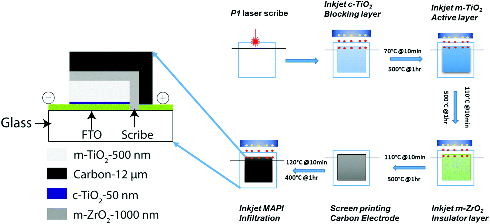 | ||
| Fig. 1 Device architecture of the MPSC with desired layer thicknesses in cross section view. Process flow demonstrating inkjet printing of four layers consisting of compact titania (c-TiO2), mesoporous titania (m-TiO2), mesoporous zirconia (m-ZrO2) and infiltration of methyl ammonium lead tri-iodide (MAPI) perovskite precursor. Yellow dots represent the print head nozzles while red dots represent the ejected droplets. | ||
In this work, we demonstrate a fully solution processed MPSC with four layers out of five inkjet printed in ambient conditions. In particular, all the metal oxide layers, i.e. c-TiO2, m-TiO2 and m-ZrO2 as well as the perovskite precursor ink were deposited by inkjet. The oxide layers and the carbon electrode were first sintered at elevated temperature and then infiltrated with the standard MAPI by inkjet at room temperature. Cells were fully characterized and compared to standard screen-printed devices. In addition, we highlight the advantages of precise, waste-free infiltration using inkjet and provide guide values for the printing speed that can be achieved by this technology. We also demonstrate highly stable and environmentally friendly inks for each of the MPSC layers using non-halogenated solvents.
Experimental
Characterization
Viscosity and density of the inks were measured on a falling ball viscometer from Anton Paar (LOVIS 2000 ME). Surface tension and wetting of the inks were characterized using a drop shape analyzer from Krüss (DSA30). Contact angle measurements for determining the wetting envelope were carried out on the individual solar cell stack layers after firing them at 500° for 1 h. The thickness of the layers was determined with a profilometer (XP-1 Surface Profilometer, Ambios Technology). The film surface was characterized by atomic force microscopy (ICON3 from Bruker) in tapping mode. The crystallization behavior of the nanoparticles as well as the perovskite formation in the mesoporous structure were analyzed by XRD (Pan Analytics, X'Pet PRO). SEM images were taken with a FEI NanoSEM 230.Solar cells were fabricated on a 10 cm × 10 cm fluorine doped tin oxide (FTO) coated glass and were cut into 18 individual cells with 1.5 cm2 active area each (Fig. S1, ESI†). Silver contacts were applied on both anode and cathode sides for current collection. The solar cells were fitted with an opaque black adhesive vinyl mask bearing a 0.64 cm2 aperture (Solaronix SA) and measured in a Solar-Sim 150 solar simulator (Solaronix SA) calibrated to 1000 W m−2. The voltage was scanned between −0.3 and 1 V, in 5 mV increments every 1.2 s. Typically, more than 5 cells were measured for each development stage of the inkjet printed stack layers. Thereof, the mean solar cell figures and standard deviations were extracted, as well as the champion cell characteristics.
Materials
For the development of a TiO2 ink allowing to obtain a homogenous and pinhole free compact layer, 75 wt% titanium diisopropoxide bis(acetylacetonate) (TAA) in isopropanol (Sigma Aldrich) was used. Titania paste Ti-Nanoxide T165/SP (Solaronix SA, Switzerland) and zirconia paste Zr-Nanoxide ZT/SP (Solaronix SA, Switzerland) were adapted for inkjet printing. The utilized carbon paste (Elcocarb B/SP) is a mixture of 25 wt% of carbon nanoparticles and graphite flakes and was used for screen-printing the top electrode. For the perovskite precursor ink, 1.2 mole of lead iodide, 1.2 mole of methylammonium iodide and 0.06 mole of-ammonium valeric acid iodide were dissolved in 1 mL of γ-butyrolactone (GBL).Device fabrication
Devices were fabricated on FTO coated glass, which was cleaned using pH neutral surfactant, acetone, isopropanol (iPrOH) and deionized water. The glasses were then dried with pressurized air and on a hot plate for 10 min at 110 °C. For the fabrication of reference MPSC devices, previously optimized thicknesses were used as follows: 50 nm c-TiO2, 500 nm m-TiO2, 1000 nm m-ZrO2, 10–12 μm porous carbon as reported.25 For reference devices, the c-TiO2 ink was deposited by spray pyrolysis, while all other layers were deposited by screen-printing using a DEK148 semi-automatic screen printer. Ti-Nanoxide T165/SP (Solaronix SA), Zr-Nanoxide ZT/SP (Solaronix SA) and Elcocarb B/SP (Solaronix SA) were printed using a 165–30, 90–48 and 43–80 mesh stencil, respectively. The screen printing inks of m-TiO2 and m-ZrO2 are composed of metal oxide nanoparticles with a diameter of 20 nm. The carbon ink consists of graphite flakes with typical dimensions of several microns and nano-particle carbon about 30 nm in size. The wet film was allowed to dwell for 10 min before drying at 120 °C for 10 min and then firing at 500 °C to remove all organic binders. Carbon was fired at 400 °C for 1 h.Inkjet printing was carried out on a PixDro LP50 printer from Meyer Burger. Various print heads were investigated for various layers ranging from lab scale Dimatix DMC11601 and DMC11610 and semi-industrial spectra S-class with 128 nozzle printhead.
Inkjet printing was developed by replacing the sprayed or screen-printed layer one by one by the corresponding inkjet printed layer. The substitution implied the c-TiO2, m-TiO2 as well as the m-ZrO2 layer. Each layer was optimized to reach comparable performance to the screen-printed cells using the standard semi-manual pipetting method for infiltrating the MAPI ink. All oxides, i.e. c-TiO2, m-TiO2 and m-ZrO2 were deposited using a spectra print-head. For the perovskite precursor a Dimatix print head was used. The line per inch (lpi) and dots per inch (dpi) values were optimized for each layer to achieve homogenous layer formation as well as to deposit a controlled liquid volume on to the substrate resulting in the adequate fired layer thickness. Drying and post annealing sequences were optimized individually. The c-TiO2 layer was first dried at 70 °C for 10 min and then heated to 500 °C for 1 h before depositing the next layer. The wet m-TiO2 and m-ZrO2 films were dried at 110 °C, both layers were fired at 500 °C for 1 h after the drying step.
The perovskite precursor was re-dissolved at 70 °C right prior to use. After deposition, the perovskite films were annealed at 50 °C for 10 min on a hot plate in ambient conditions.
Results and discussion
Ink formulation and inkjet deposition
As commonly used in the PSC field, a compact titania blocking layer (c-TiO2) was first deposited on FTO coated glass.29 The homogeneity of this layer is critical to device performance, since it has to inhibit possible short circuits caused by pinholes in the oxide over layers. Compact titania is generally deposited using spin coating,30,31 spray pyrolysis,32 sputtering33 or atomic layer deposition.34 Inkjet printing the compact layer is challenging due to hydrolysis of the sol–gel precursor ink in ambient condition, which can lead to clogging of the nozzles. Such effects have indeed been described for the inkjet deposition of thin photocatalytic TiO2 layers.35 Furthermore, depositing a thin homogeneous and continuous film on the rough FTO surface, without crack or pinhole formation is delicate. Commercially available slot die coating ink from Solaronix (Ti-Nanoxide BL150/DC) is closest to inkjet ink requirements and thus was tested for inkjet printing. We were able to get a continuous printed wet film, but upon drying the film destabilized and became inhomogeneous. We also observed particle formation at the nozzle plate when jetting was prolonged for several hours. We thus formulated a new ink starting from the TAA stock solution using an appropriate dilution with binary mixtures such as ethylene glycol:isopropanol, tetralin:isopropanol, terpineol:isopropanol, ethylene glycol:ethanol, tetralin:ethanol, terpineol:ethanol (see ESI†). Advantageously, all binary systems lie within the wetting envelope of the FTO substrate (Fig. 2a) and therefore ensure excellent wet layer formation. The c-TiO2 ink using 1![[thin space (1/6-em)]](https://www.rsc.org/images/entities/char_2009.gif) :15 vol/vol of TAA into binary solvent yielded a homogeneous and pinhole free layer of 60 nm in thickness after firing at 500 °C for 1 h. The printing was done in a two-pass wet on wet deposition sequence without drying steps between the two deposition steps.
:15 vol/vol of TAA into binary solvent yielded a homogeneous and pinhole free layer of 60 nm in thickness after firing at 500 °C for 1 h. The printing was done in a two-pass wet on wet deposition sequence without drying steps between the two deposition steps.
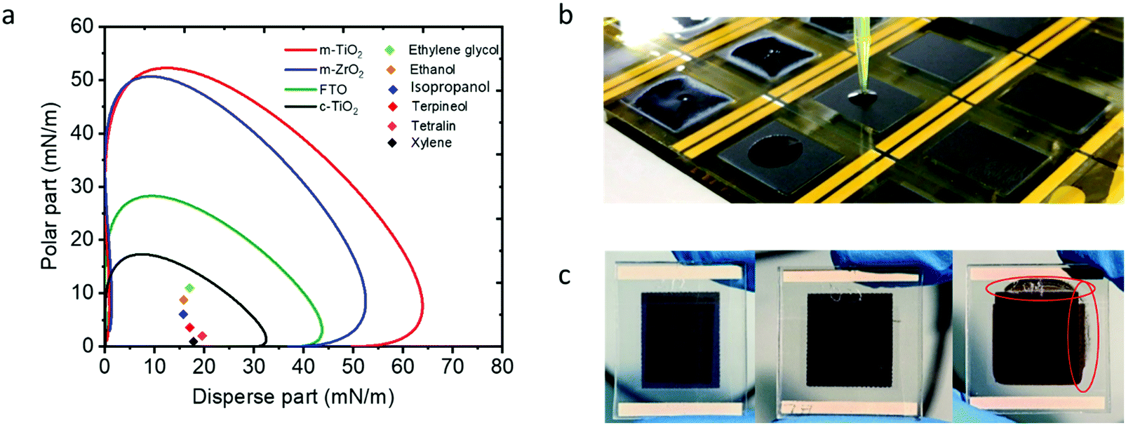 | ||
| Fig. 2 Wetting envelopes of the various surfaces of the MPSC stack, which are relevant for the deposition of printable inks. Surface energies of the various solvents used to develop printable inks lie inside the wetting envelope of the different oxides and fluorine doped tin oxide (FTO) and therefore predict good wetting behavior (a). Conventional infiltration of MAPI precursor solution by semi-automatic pipetting method (b) and by inkjet infiltration (c) showing under-filling (left), ideal filling (middle) and overfilling (right, marked in red). | ||
Spin coating, screen-printing and slot die coating of the m-TiO2 layer has been reported in various perovskite solar cell architectures.16 Inkjet printing of thin mesoporous oxide layers (80–100 nm) in planar perovskite solar cell device architectures has been reported using a Dimatix printhead with multipass printing.26 Here a jettable m-TiO2 ink was developed by diluting the commercial screen printing paste (Solaronix SA) using a binary solvent mixture (see ESI,† Fig. S2). Using the reported recipe26 and process to reach 500 nm of dried thickness with increasing the number of passes would imply too thick wet films leading to uncontrolled spreading beyond the c-TiO2 coated area, which can lead to shunting of the solar cell. Therefore, to reach a thickness of 500 nm, a two-pass wet inkjet deposition was employed with subsequent drying steps of 110 °C for 10 min. Eventually the m-TiO2 layer was sintered at 500 °C for 1 h.
Inkjet printing of zirconia nanoparticle inks have not been reported to the best of our knowledge. The challenge is to formulate a stable nanoparticle dispersion, which does not clog the nozzles and has high enough concentration to form a 1000 nm thick layer after firing at 500 °C. We followed a similar binary solvent strategy as used for m-TiO2 ink development. The spectra printhead was used for obtaining important wet thicknesses required to reach the targeted layer thickness. The screen printing paste from Solaronix was diluted with binary solvent mixtures (see ESI,† Fig. S2), which all fall in the stable wetting envelope as shown in Fig. 2a. Series of concentrations and ratios of solvent mixtures were screened. The binary solvent ink gave stable jetting with no satellite formation as well as homogenous film formation (ESI,† Fig. S1 and S2). The wet films were dried on a hot plate for 10 min at 110 °C in ambient condition and subsequently fired at 500 °C for 1 h before receiving the carbon layer.
Infiltration of methyl ammonium lead tri-iodide (MAPI)
Inkjet printing of the perovskite precursor solution provides a novel method to infiltrate MPSC. It is a precise and waste free deposition technique as well as clean deposition method. Precise volume control and drop placement promises device-to-device reproducibility as well as performance. The clear advantage of inkjet deposition over pipette infiltration is illustrated in Fig. 2b and c. Semiautomatic pipetting has the disadvantage of considerable liquid thickness variations with a larger liquid volume in the centre of the device. Upon drying, this leads to a deterioration of the upper layers of the carbon electrode. Also it is impossible to achieve a precise edge definition. However, using inkjet deposition, precise volumes of ink can be deposited with high spatial resolution. Inkjet printing of the perovskite precursor has been reported by Hashmi et al.26 for MPSC with power conversion efficiencies of 8.5% for an active area 0.16 cm2. Here the same ink recipes were adopted and further optimized with respect to the filling of the mesoporous structure by varying ink volumes, optimizing dpi and lpi as well as other jetting parameters (see ESI†). We found that the filling conditions are quite resilient, allowing ink volumes from 3–4.5 μL per cell, which can be achieved by a two pass or three pass process (Table S3, ESI†). Following infiltration and drying, the devices were post-treated in damp heat for 100 h. This treatment increases the crystallinity of the perovskite layer as was determined by X-ray diffraction (ESI,† Fig. S5). After optimizing the drying process following infiltration, high PCEs exceeding 13% for a device area of 1.5 cm2 with 0.64 cm2 aperture (Table 1 and Table S3, ESI†) could be achieved on the sprayed and screen printed reference stack. This is significantly higher than the previously reported PCE of 8.5% using a four times smaller aperture area.26 Interestingly, partial MAPI infiltration allowed to assess the crucial importance of the thick mesoporous layers on absorber stability. At low filling volumes, the cells turned yellow after three months of exposure to ambient atmosphere, revealing the transformation of the perovskite into PbI2. But fully infiltrated stacks remained black, hinting at the formation of a passivation layer protecting the active perovskite material underneath (ESI,† Fig. S6a).| Inkjet printed layer | Print pass | V oc (V) | J sc (mA cm−2) | FF (%) | PCE (%) |
|---|---|---|---|---|---|
| Reference device | 1× | 0.92 | 23.7 | 66.1 | 12.9 |
| c-TiO2 | 2× | 0.87 ± 0.04 (0.87*) | 19.1 ± 3.0 (22*) | 57.7 ± 1.2 (57.7*) | 9.9 ± 1.8 (11.1*) |
| m-TiO2 | 2× | 0.87 ± 0.01 (0.86*) | 13.5 ± 3.6 (12.9*) | 68.2 ± 11.1 (77.6*) | 8.5 ± 1.8 (8.7*) |
| c-TiO2 and m-TiO2 | As above | 0.86* | 17.8* | 65.6* | 10.2* |
| m-ZrO2 | 3× | 0.9 ± 0.03 (0.9*) | 18.7 ± 0.8 (19.1*) | 70.1 ± 1.5 (71.8*) | 11.9 ± 0.7 (12.4*) |
| MAPbI3 | 1×, 2× | 0.96 ± 0.01 (0.96*) | 20.2 ± 0.5 (20.8*) | 67.4 ± 0.7 (67*) | 12.9 ± 1.0 (13.5*) |
| c-TiO2, m-TiO2, m-ZrO2 and MAPbI3 | As above | 0.92 ± 0.02 (0.9*) | 14.4 ± 1.6 (17.2*) | 68.5 ± 4.7 (59*) | 8.7 ± 0.8 (9.1*) |
Inkjet printing for all the oxides as well as the perovskite ink was carried out at a speed of 200 mm s−1 with multi swath and multipass printing as stated in Table 1. Using such printing speed allows to print the 18-cell design shown in Fig. S1 of the ESI† with two passes in about 4 minutes.
Device fabrication and characterization
Optimized MPSC today reach efficiencies of 15–17%36 on the lab scale. To bring this technology to an industrial level, however, reproducible large area fabrication has to be developed. Besides the recurrent issue of defects and pinholes coming along with increasing the active area, problems associated with large area are the homogeneity of the layers in terms of thickness and crystallinity. Of particular interest are cell areas of the order of 1 cm2, since they are relevant to the length scale used in series connection geometries applied in modules. There are several encouraging reports where cell areas of 1 cm2 or more with efficiencies of 12–19% have been achieved.37 Large area modules of more than 10 to 100 cm2 have also been reported with active area efficiencies ranging from 5–15%.38,39 As pointed out in the perspective article by Rong et al., the most appropriate technique for large area fabrication is slot die coating.40 However, this technique is less well suited for customizing the shape of the active area. Our goal was to reach customizable cells on large area using digital inkjet printing. Albeit the challenges brought about by inkjet printing thick nanoparticle layers, we chose the MPSC architecture, because it is more resilient towards pinholes and allows convenient infiltration of the perovskite absorber ink. To date MPSC also reveal the longest lifetime of more than 1 year.41The printing parameters were first optimized for the individual oxide layers on glass substrates. Large area film homogeneity was assessed by visual inspection, both in the wet and dry state. For the scattering mesoporous oxide layers, the degree of opaqueness can easily be detected by eye as shown in Fig. S1(c) and (d) (ESI†). For the ultrathin c-TiO2 layer, visual inspection is carried out at a certain tilt angle, where interference fringes can be observed. On a smaller scale of 3.5 × 3.5 μm, we performed atomic force microscopy (AFM) scans (ESI,† Fig. S3). We extracted line scans in order to visualize the surface roughness of the oxide films (ESI,† Fig. S4). Typical roughness values of 10 nm and 15 nm, were obtained for m-TiO2 and m-ZrO2, respectively, showing smooth and continuous films with respect to the nano-particulate nature of the inks and the layer thicknesses. Ultrathin c-TiO2 films, however, present dewetting features.
In order to evaluate the quality of the screen-printed layers, we proceeded stepwise and used the screen printed cell as a reference. Each layer of the device stack (except carbon) was then replaced by an inkjet printed layer to verify its functionality within the stack. Note that if not otherwise indicated, the perovskite ink infiltration was carried out by pipetting 5.7 μL of perovskite ink per cell area of 1.5 cm2. There are several conclusions that can be drawn from this study. As can be inferred from Table 1, the infiltration of MAPI using inkjet performs as well as the pipetting method. This is a very encouraging result, since inkjet infiltration can potentially be used to screen different perovskite precursor inks and to study additives in a convenient systematic way. Replacing the screen printed titania layers by inkjet printed layers did however affect the power conversion efficiency (PCE) to some extent. This may be due to the reduced thickness obtained for m-TiO2 using inkjet. While the layer thicknesses were optimized on glass to achieve a thickness of 500 nm after firing, the thickness of m-TiO2 obtained in the device as measured by SEM is around 350–400 nm (see Fig. 3). The lower thickness obtained in the MPSC stack may be due to the different wetting behavior of glass and c-TiO2. Additionally the FTO roughness adds to the thickness variation of m-TiO2 in the device. This means that the absorber layer is thinner than in the reference device and consequently, the photoinduced charge carrier generation decreases. The fact that the short circuit current density was most affected by inkjet printing m-TiO2 underlines this reasoning.
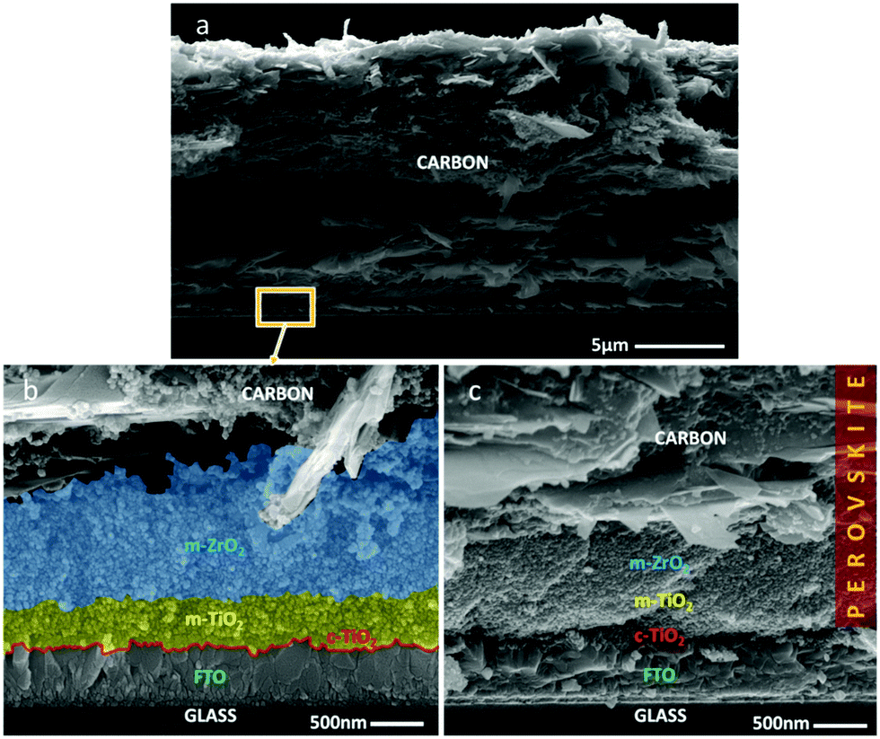 | ||
| Fig. 3 SEM images of inkjet printed MPSC cell cross sections showing the three oxide layers, fluorine doped tin oxide (FTO) as well as the thick carbon electrode (a). For clarity, the zoom-in picture is colored and shows the cross-section of a non-infiltrated stacks (b) and a stack infiltrated with perovskite (c). | ||
Inkjet printing the c-TiO2 layer mainly affects the fill factor of the device. The reason could be related to the difficulty to obtain such an ultrathin continuous layer on a rough FTO substrate. AFM images indeed confirm thickness inhomogeneities of the inkjet printed c-TiO2 layer (ESI,† Fig. S3a). It is likely that spray pyrolysis employed in the reference device is superior in this respect. Inkjet printing the m-ZrO2 layer gave very similar results as for the reference device. The latter layer acts merely as a space holder to avoid direct contact between the carbon electrode and m-TiO2 and therefore its effect is less sensitive.
Eventually, we achieved a large area (full area of 1.5 cm2) solar cell with a PCE of 9.1% measured with an aperture of 0.64 cm2, where all oxide layers and the perovskite absorber were deposited by inkjet (Fig. 4). The current–voltage (J–V) characteristics show rather small hysteresis, even though some efficiency loss is observed as compared to the screen printed reference device. As discussed, the lower short circuit current density Jsc hints towards a reduced active layer thickness as compared to the reference device. Very likely, the lower fill factor may be related to the difficulty of inkjet printing an ultrathin pinhole-free c-TiO2 layer. At this stage, the fully inkjet printed solar cell bears a lot of optimization potential. A thorough investigation of the device physics is still missing and has to be carried out in forthcoming work.
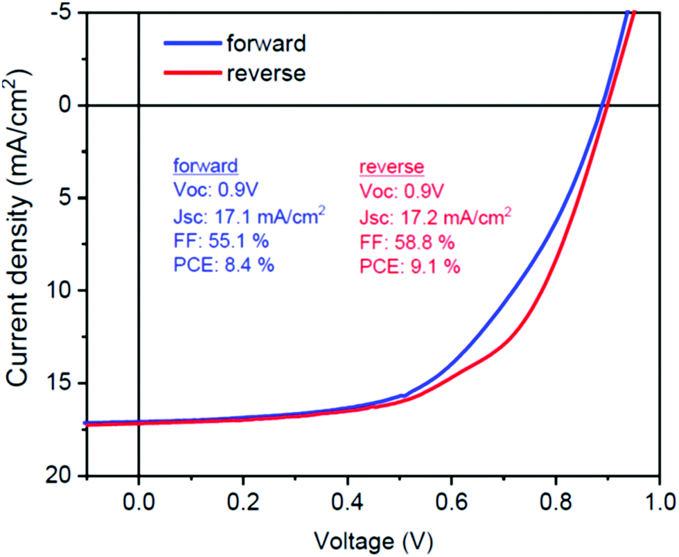 | ||
| Fig. 4 J–V characteristics of a photovoltaic cell with an area of 1.5 cm2 with four layers of the stack deposited by inkjet printing. The device shows little hysteresis from reverse to forward scan. | ||
We undertook first attempts to also inkjet print the top electrode using ITO and carbon inks (see ESI,† Table S4). This preliminary attempts yielded rather poor efficiencies below 1%. Further developments in this direction will be addressed in future work.
Conclusions
In this work, we achieved inkjet printed carbon based solar cells with four layers out of five being inkjet deposited using environment friendly non-halogenated solvents. This includes all oxide layers, i.e. c-TiO2, m-TiO2, m-ZrO2 as well as the perovskite precursor ink. We have demonstrated extensive ink development of nanoparticles for stable jetting and wetting as well as MPSC device performance. We demonstrated large area solar cell devices with an efficiency of 9.1%. If the organo-metal iodide (MAPI) ink was infiltrated into reference monolithic stacks produced by screen printing, we achieved a power conversion efficiency of 13.5%, which is a breakthrough for a device area larger than 1 cm2. Given the fact that inkjet technology is scalable, there are high prospects for printing larger device areas. Furthermore, inkjet printing enables customized complex cell geometries for specific applications, such as personal wearable or small utility power sources as well as building integrated photovoltaics. Inkjet printing of carbon and metal oxides for electrodes remain a challenge and requires further ink and process development.Conflicts of interest
There are no conflicts of interest to declare.Acknowledgements
Financial support of this work be the Swiss Federal Office of Energy (grant no. SI/501816-01) is gratefully acknowledged. We acknowledge the use of the facilities of the Coating Competence Center (CCC) and the Swiss Scanning Probe Microscopy User Lab (SUL) at Empa.References
- Trends in Photovoltaic Applications, Report IEA PVPS 2018, T1-34:2018.
- M. Valimaki, E. Jansson, P. Korhonen, A. Peltoniemi and S. Rousu, Custom-Shaped Organic Photovoltaic Modules-Freedom of Design by Printing, Nanoscale Res. Lett., 2017, 12, 117 CrossRef CAS PubMed.
- D. K. Gupta, M. Langelaar, M. Barink and F. van Keulen, Optimizing front metallization patterns: Efficiency with aesthetics in free-form solar cells, Renewable Energy, 2016, 86, 1332–1339 CrossRef.
- D. E. Attoye, K. A. T. Aoul and A. Hassan, A Review on Building Integrated Photovoltaic Facade Customization Potentials, Sustainability, 2017, 9, 2287 CrossRef.
- D. A. Hardy, S. C. Roaf and B. S. Richards, Improving the aesthetics of photovoltaics in decorative architectural glass, WIT Trans. Built Environ., 2014, 142, 1743–3509 Search PubMed.
- S. Roberts and N. Guariento, Building integrated photovoltaics: a handbook, Birkäuser Verlag AG, Basel, 2009 Search PubMed.
- W. Zapka, Handbook of Industrial Inkjet Printing: A Full System Approach, Weinheim, Wiley-VCH, 2018 Search PubMed.
- M. Singh, H. M. Haverinen, P. Dhagat and G. E. Jabbour, Inkjet Printing-Process and Its Applications, Adv. Mater., 2010, 22, 673–685 CrossRef CAS PubMed.
- Y. T. Gizachew, L. Escoubas, J. J. Simon, M. Pasquinelli, J. Loiret, P. Y. Leguen, J. C. Jimeno, J. Martin, A. Apraiz and J. P. Aguerre, Towards ink-jet printed fine line front side metallization of crystalline silicon solar cells, Sol. Energy Mater. Sol. Cells, 2011, 95, S70–S82 CrossRef CAS.
- X. Z. Lin, R. Klenk, L. Wang, T. Kohler, J. Albert, S. Fiechter, A. Ennaoui and M. C. Lux-Steiner, 11.3% efficiency Cu(In,Ga)(S,Se)(2) thin film solar cells via drop-on-demand inkjet printing, Energy Environ. Sci., 2016, 9, 2037–2043 RSC.
- X. Z. Lin, V. E. Madhavan, J. Kavalakkatt, V. Hinrichs, I. Lauermann, M. C. Lux-Steiner, A. Ennaoui and R. Klenk, Inkjet-printed CZTSSe absorbers and influence of sodium on device performance, Sol. Energy Mater. Sol. Cells, 2018, 180, 373–380 CrossRef CAS.
- T. M. Eggenhuisen, Y. Galagan, A. Biezemans, T. Slaats, W. P. Voorthuijzen, S. Kommeren, S. Shanmugam, J. P. Teunissen, A. Hadipour, W. J. H. Verhees, S. C. Veenstra, M. J. J. Coenen, J. Gilot, R. Andriessen and W. A. Groen, High efficiency, fully inkjet printed organic solar cells with freedom of design, J. Mater. Chem. A, 2015, 3, 7255–7262 RSC.
- C. N. Hoth, P. Schilinsky, S. A. Choulis and C. J. Brabec, Printing highly efficient organic solar cells, Nano Lett., 2008, 8, 2806–2813 CrossRef CAS PubMed.
- S. Jung, A. Sou, K. Banger, D. H. Ko, P. C. Y. Chow, C. R. McNeill and H. Sirringhaus, All-Inkjet-Printed, All-Air-Processed Solar Cells, Adv. Energy Mater., 2014, 4, 1400432 CrossRef.
- S. G. Hashmi, M. Ozkan, J. Halme, K. D. Misic, S. M. Zakeeruddin, J. Paltakari, M. Gratzel and P. D. Lund, High performance dye-sensitized solar cells with inkjet printed ionic-liquid electrolyte, Nano Energy, 2015, 17, 206–215 CrossRef CAS.
- S. G. Hashmi, M. Ozkan, J. Halme, S. M. Zakeeruddin, J. Paltakari, M. Gratzel and P. D. Lund, Dye-sensitized solar cells with inkjet-printed dyes, Energy Environ. Sci., 2016, 9, 2453–2462 RSC.
- R. Cherrington, D. J. Hughes, S. Senthilarasu and V. Goodship, Inkjet-Printed TiO2 Nanoparticles from Aqueous Solutions for Dye-Sensitized Solar Cells (DSSCs), Energy Technol., 2015, 3, 866–870 CrossRef CAS.
- Y. G. Rong, Y. Hu, A. Y. Mei, H. R. Tan, M. I. Saidaminov, S. I. Seok, M. D. McGehee, E. H. Sargent and H. W. Han, Challenges for commercializing perovskite solar cells, Science, 2018, 361, eaat8235 CrossRef PubMed.
- C. Liang, P. W. Li, H. Gu, Y. Q. Zhang, F. Y. Li, Y. L. Song, G. S. Shao, N. Mathews and G. C. Xing, One-Step Inkjet Printed Perovskite in Air for Efficient Light Harvesting, Sol. RRL, 2018, 2, 1700217 CrossRef.
- F. Mathies, H. Eggers, B. S. Richards, G. Hernandez-Sosa, U. Lemmer and U. W. Paetzold, Inkjet-Printed Triple Cation Perovskite Solar Cells, ACS Appl. Energy Mater., 2018, 1, 1834–1839 CrossRef CAS.
- P. W. Li, C. Liang, B. Bao, Y. N. Li, X. T. Hu, Y. Wang, Y. Q. Zhang, F. Y. Li, G. S. Shao and Y. L. Song, Inkjet manipulated homogeneous large size perovskite grains for efficient and large-area perovskite solar cells, Nano Energy, 2018, 46, 203–211 CrossRef CAS.
- Z. H. Wei, H. N. Chen, K. Y. Yan and S. H. Yang, Inkjet Printing and Instant Chemical Transformation of a CH3NH3PbI3/Nanocarbon Electrode and Interface for Planar Perovskite Solar Cells, Angew. Chem., Int. Ed., 2014, 53, 13239–13243 CrossRef CAS PubMed.
- A. J. Huckaba, Y. Lee, R. Xia, S. Paek, V. C. Bassetto, E. Oveisi, A. Lesch, S. Kinge, P. J. Dyson, H. Girault and M. K. Nazeeruddin, Inkjet-Printed Mesoporous TiO2 and Perovskite Layers for High Efficiency Perovskite Solar Cells, Energy Technol., 2019, 7, 317–324 CrossRef CAS.
- Y. G. Rong, Z. L. Ku, A. Y. Mei, T. F. Liu, M. Xu, S. G. Ko, X. Li and H. W. Han, Hole-Conductor-Free Mesoscopic TiO2/CH3NH3PbI3 Heterojunction Solar Cells Based on Anatase Nanosheets and Carbon Counter Electrodes, J. Phys. Chem. Lett., 2014, 5, 2160–2164 CrossRef CAS PubMed.
- G. Grancini, C. Roldan-Carmona, I. Zimmermann, E. Mosconi, X. Lee, D. Martineau, S. Narbey, F. Oswald, F. De Angelis, M. Graetzel and M. K. Nazeeruddin, One-Year stable perovskite solar cells by 2D/3D interface engineering, Nat. Commun., 2017, 8, 15684 CrossRef CAS PubMed.
- S. G. Hashmi, A. Tiihonen, D. Martineau, M. Ozkan, P. Vivo, K. Kaunisto, V. Ulla, S. M. Zakeeruddin and M. Gratzel, Long term stability of air processed inkjet infiltrated carbon-based printed perovskite solar cells under intense ultra-violet light soaking, J. Mater. Chem. A, 2017, 5, 4797–4802 RSC.
- X. J. Peng, J. Yuan, S. Shen, M. Gao, A. S. R. Chesman, H. Yin, J. S. Cheng, Q. Zhang and D. Angmo, Perovskite and Organic Solar Cells Fabricated by Inkjet Printing: Progress and Prospects, Adv. Funct. Mater., 2017, 27, 1703704 CrossRef.
- S. K. Karunakaran, G. M. Arumugam, W. T. Yang, S. J. Ge, S. N. Khan, X. Z. Lin and G. W. Yang, Recent progress in inkjet-printed solar cells, J. Mater. Chem. A, 2019, 7, 13873–13902 RSC.
- E. J. Juarez-Perez, M. Wussler, F. Fabregat-Santiago, K. Lakus-Wollny, E. Mankel, T. Mayer, W. Jaegermann and I. Mora-Sero, Role of the Selective Contacts in the Performance of Lead Halide Perovskite Solar Cells, J. Phys. Chem. Lett., 2014, 5, 680–685 CrossRef CAS PubMed.
- Y. Hou, H. Zhang, W. Chen, S. Chen, C. O. R. Quiroz, H. Azimi, A. Osvet, G. J. Matt, E. Zeira, J. Seuring, N. Kausch-Busies, W. Lovenich and C. J. Brabec, Inverted, Environmentally Stable Perovskite Solar Cell with a Novel Low-Cost and Water-Free PEDOT Hole-Extraction Layer, Adv. Energy Mater., 2015, 5, 7 Search PubMed.
- M. Z. Liu, M. B. Johnston and H. J. Snaith, Efficient planar heterojunction perovskite solar cells by vapour deposition, Nature, 2013, 501, 395–398 CrossRef CAS PubMed.
- A. Mollmann, D. Gedamu, P. Vivo, R. Frohnhoven, D. Stadler, T. Fischer, I. Ka, M. Steinhorst, R. Nechache, F. Rosei, S. G. Cloutier, T. Kirchartz and S. Mathur, Highly Compact TiO2 Films by Spray Pyrolysis and Application in Perovskite Solar Cells, Adv. Eng. Mater., 2019, 21, 1801196 CrossRef.
- W. J. Ke, G. J. Fang, J. Wang, P. L. Qin, H. Tao, H. W. Lei, Q. Liu, X. Dai and X. Z. Zhao, Perovskite Solar Cell with an Efficient TiO2 Compact Film, ACS Appl. Mater. Interfaces, 2014, 6, 15959–15965 CrossRef CAS PubMed.
- Y. Z. Wu, X. D. Yang, H. Chen, K. Zhang, C. J. Qin, J. Liu, W. Q. Peng, A. Islam, E. B. Bi, F. Ye, M. S. Yin, P. Zhang and L. Y. Han, Highly compact TiO2 layer for efficient hole-blocking in perovskite solar cells, Appl. Phys. Express, 2014, 7, 4 Search PubMed.
- M. Cerna, M. Vesely and P. Dzik, Physical and chemical properties of titanium dioxide printed layers, Catal. Today, 2011, 161, 97–104 CrossRef CAS.
- Y. G. Rong, X. M. Hou, Y. Hu, A. Y. Mei, L. F. Liu, P. Wang and H. W. Han, Synergy of ammonium chloride and moisture on perovskite crystallization for efficient printable mesoscopic solar cells, Nat. Commun., 2017, 8, 14555 CrossRef PubMed.
- L. L. Gao, L. Chen, S. Y. Huang, X. L. Li and G. J. Yangu, Series and Parallel Module Design for Large-Area Perovskite Solar Cells, ACS Appl. Energy Mater., 2019, 2, 3851–3859 CrossRef CAS.
- A. L. Palma, F. Matteocci, A. Agresti, S. Pescetelli, E. Calabro, L. Vesce, S. Christiansen, M. Schmidt and A. Di Carlo, Laser-Patterning Engineering for Perovskite Solar Modules With 95% Aperture Ratio, IEEE J. Photovolt., 2017, 7, 1674–1680 Search PubMed.
- L. H. Cai, L. S. Liang, J. F. Wu, B. Ding, L. Gao and B. Fan, Large area perovskite solar cell module, J. Semicond., 2017, 38, 14006 CrossRef.
- Y. G. Rong, Y. Ming, W. X. Ji, D. Li, A. Y. Mei, Y. Hu and H. W. Han, Toward Industrial-Scale Production of Perovskite Solar Cells: Screen Printing, Slot-Die Coating, and Emerging Techniques, J. Phys. Chem. Lett., 2018, 9, 2707–2713 CrossRef CAS PubMed.
- S. G. Hashmi, D. Martineau, X. Li, M. Ozkan, A. Tiihonen, M. I. Dar, T. Sarikka, S. M. Zakeeruddin, J. Paltakari, P. D. Lund and M. Gratzel, Air Processed Inkjet Infiltrated Carbon Based Printed Perovskite Solar Cells with High Stability and Reproducibility, Adv. Mater. Technol., 2017, 2, 1600183 CrossRef.
Footnote |
| † Electronic supplementary information (ESI) available. See DOI: 10.1039/d0ma00077a |
| This journal is © The Royal Society of Chemistry 2020 |