
 Open Access Article
 This Open Access Article is licensed under a Creative Commons Attribution-Non Commercial 3.0 Unported Licence
Crystallographic phase changes and damage thresholds of CsPbI3 microwire waveguides through continuous wave photoablation†
Kieran O.
Russell
a,
Mark A.
Osborne
 *b and
Aidan A. E.
Fisher
*b
*b and
Aidan A. E.
Fisher
*b
aDepartment of Chemistry, University of Cambridge, UK
bDepartment of Chemistry, University of Sussex, Falmer, UK. E-mail: m.osborne@sussex.ac.uk; aidan.fisher@sussex.ac.uk
First published on 23rd April 2020
Abstract
We investigate waveguide efficiency of CsPbI3 microwire waveguides and their photodegradation over a range of continuous wave laser excitation energies and intensities. Under modest laser input intensities <1 kW cm−2 we observe a wavelength dependent efficiency of light propagation in the waveguides. At increased power densities and wavelengths of 473 nm or shorter, microwires undergo photoablation into discrete fragments. Use of diffraction-limited excitation allowed localised cleavage of the microwires with observation of transient photoluminescence from degradation products. TEM analysis of the microwires revealed transformation from the yellow δ-phase to amorphous phases in the region of the photodamage with a degraded morphology consistent with efficient thermal transfer and induced melting.
The use of waveguides to carry optical frequencies was pioneered by Kao et al. during the 1960s and has since become state-of-the-art technology for broadband delivery world-wide.1 At the opposite end of the size spectrum, optical circuits show promise to deliver a next-generation alternative to electronics in areas as diverse as solar concentrators,2–5 optical computing and chemical sensing.6,7 Nanowire (NW) waveguides offer routes to miniaturization of components and devices and a number of semiconductor nanomaterials including CdS and InP NWs, have been shown to exhibit good waveguide properties.8 Early work by Lieber et al. reports on waveguide efficiency in CdS NWs as a function of input light coupling geometries.9,10 While more recently Assefa and co-workers have demonstrated the integration of Si NWs, optical transmitters and receivers in a CMOS-integrated nanophotonic “computer” chip as a route to preserving Moore's Law.11 Presently, there are several reports of 1D NW structures, both organic and inorganic, which are able to effectively propagate light.12,13 All-inorganic lead halide perovskite NWs have previously been shown to behave as Fabry–Pérot lasing cavities by exploiting the strong photoluminescence (PL) properties of the cubic, α-phase and its highly crystalline facets.14–16 Their unique emission tunability and long-term stability compared with their organic counterparts has made them particularly attractive across a range of applications.13,17
In this communication we report on the efficiency of non-emitting, δ-phase CsPbI3 microwires (MWs) as waveguides and their stability at a variety of wavelengths, intensities and input light positions. Synthesized using established colloidal methods,18 the MWs offer typical dimensions in the range 10–40 μm in length, but sub-micron widths around 500–1000 nm (Fig. 1a). The UV-Vis absorption spectrum of yellow δ-phase, CsPbI3 MWs (suspended in hexane) showed confinement of the first exciton to a weak band peaking at 390 nm with strong, bulk-band absorption at shorter wavelengths (Fig. 1b). The corresponding Tauc plot (Fig. 1b inset) revealed an extrapolated absorption onset at 3.04 eV (408 nm) for these MWs, in good agreement with other reports on the δ-phase system19 and strongly blue-shifted from the black, PL-active phase which exhibits a band gap around 1.7 eV.20
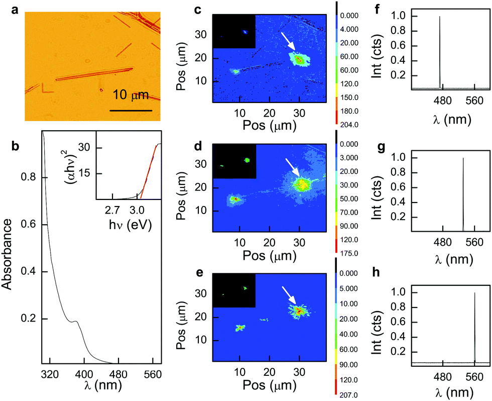 | ||
| Fig. 1 (a) Image of a single CsPbI3 MW on an optical microscope. (b) Normalized UV-Vis data of the perovskite MWs. The MWs exhibit broad absorption below 400 nm with a first-exciton peak at 390 nm. The inset is the corresponding Tauc plot which shows a transition onset of 3.04 eV. (c–e) Contour plots of the waveguide action of the MW using 473, 532 and 561 nm beams (top-bottom). The arrow indicates the laser position. Insets shows optical images of the MW at the various wavelengths. (f–h) Spectrum of the light emerging from the microwire following propagation through the crystal using the 473, 532 and 561 nm beams (top-bottom). | ||
The MWs reported here do not exhibit measurable PL until photodegraded at above band-gap laser excitation energies and high intensities. Instead, for moderate laser power densities (<1 kW cm−2) and light focused at the tip of the MW, pristine waveguides were seen to exclusively propagate light end-to-end across the wavelength range 473 nm to 561 nm (Fig. 1c–e). Output light from the MW waveguide was analysed on a microscope-coupled fibre spectrometer for the presence of residual PL. Spectra at all input wavelengths demonstrate the exclusive propagation of the monochromatic laser source with no measurable PL emission from the MW (Fig. 1f–h).
To measure transmission efficiencies across the wavelength range studied, laser input powers were attenuated well below the damage threshold, typically 0.5 kW cm−2. Light propagation was found to increase with laser wavelength; 473 nm, 532 nm and 561 nm lasers recording 9.2, 19.1 and 21.1% light transmission respectively. Attenuation coefficients for each wavelength were calculated to be 0.52, 0.36 and 0.33 dB μm−1 for 473, 532 and 561 nm light. Efficiency of the waveguide was calculated for each wavelength by integrating the intensity of light across footprints at the input and output ends of the MW and measurements were made on the same MW to mitigate against variations in size or morphology that may affect waveguide performance. The waveguide efficiencies reported here compare favourably against a variety of methyl ammonium lead halide perovskite MWs, which typically exhibit efficiencies of about 10% over a 40 micron propagation distance.21 They attribute the superior waveguide efficiency of the MAPbI3 analogue to fewer compositional inhomogeneities and less defects compared with MAPbBr3 and MAPbIxBr3−x. More recent work by Zhao et al. investigates the light propagation efficiency of organic triazatruxene MWs reporting efficiencies of 50% for 35 micron wires.22 Results for the 561 nm laser showed evidence of secondary light emission at a midpoint along the waveguide (Fig. 1e), indicative of a defect or structural anomaly. Interestingly, electron microscopy revealed MWs form from the clustering of a number of thin (50–100 nm) NWs, in whole or in part (Fig. S1, ESI†). In this case, termination of constituent NWs along the bulk MW could provide guided routes for light to couple out of the MW at points along the waveguide, other than the tips. Increased transmission at longer wavelengths is not wholly unexpected and consistent with decreasing absorption observed for the MW at energies below the band onset (Fig. 1b). Moreover, at wavelengths shorter than 473 nm, we observe poor waveguide behaviour and MWs are observed to photodegrade even at moderate laser intensities of ≈5 kW cm−2.
Despite the increased structural robustness previously reported, we found that our CsPbI3 MWs could be readily cleaved using a CW laser, focused near the diffraction-limit (Fig. S2, ESI†), at power densities >5 kW cm−2 and wavelengths of 405 nm and 448 nm. Here, the 405 nm (3.05 eV) laser excites above the 3.04 eV band-gap, while the 448 nm (2.76 eV) line sits within the Urbach tail of the absorption band, where lattice disorder and/or defect states may provide assisted excitation. We suggest the correlation between decomposition and absorption supports a charge-carrier driven photodegradation processes consistent with redox mechanisms proposed elsewhere.23 In these mechanisms, photogenerated holes ultimately lead to oxidation of the halide and loss of the halogen through sublimation, with the concomitant reduction of Pb2+ by photoelectrons and subsequent print-out of the metal. The processes account for observations of increased ion mobility in metal halide perovskite films under illumination through vacancy formation with halide loss and forms the basis of early photography with silver halide.24
Populations of MWs were tested for photodecomposition across the full wavelength range 405 nm to 561 nm as a function of intensity (Fig. 2a). At wavelengths 532 nm and longer, no photoablation was observed over the entire power range up to 40 kW cm−2. At 473 nm, MWs were found stable below 10 kW cm−2, but significant numbers were cleaved at higher powers. Only 448 nm and 405 nm lasers induced degradation in increasing fractions of MWs over intensities in the range 1–10 kW cm−2. We note transient red fluorescence is commonly observed as a feature of photodegradation at shorter wavelengths (Fig. 2b–d). Measurement of the dispersed spectra shows narrow band emission centred at 695 nm (FWHM 31 nm) (Fig. 2e) and comparable to that often reported for the α-phase CsPbI3 perovskite.18 Thermal treatment of yellow δ-phase has recently been investigated using differential scanning calorimetry to track conversion to the black, fluorescent phase with transition temperatures reported around 325 °C.25,26 Observations of fluorescence upon photocleavage in this case suggests a thermally activated δ-to-α phase change, likely induced by excited charge-carrier lattice interactions.27 Strong electron–phonon coupling through polaron formation has been invoked to account for the long carrier lifetimes that give high photoconductivities and superior performance in perovskites solar cells (PSCs).28 Furthermore phonon bottlenecks and poor energy dissipation due to low thermal conductivity is thought to slow carrier relaxation and force up-conversion of low energy lattice vibrations.29
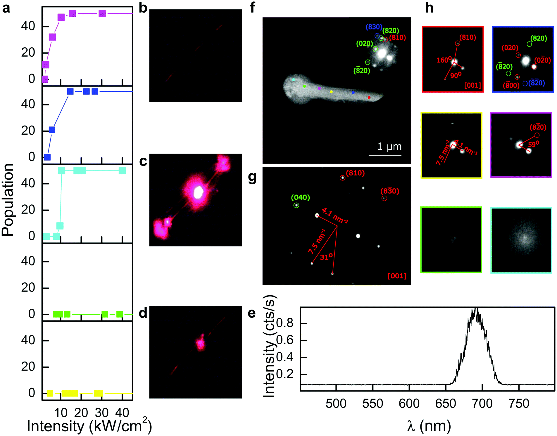 | ||
| Fig. 2 (a) Population of MWs cleaved by the laser at varying intensities and wavelengths 405 (magenta), 448 (blue), 473 (cyan), 532 (green) and 561 nm (yellow). A weak correlation exists between photocleavage and wavelength at less than 532 nm. (b–d) Structurally intact MW (top), MW undergoing laser ablation (centre) and post ablation (bottom). (e) PL spectrum collected from the microwire during photoablation. (f) δ-Phase MW which has undergone laser treatment at the bulbous end. HAADF shows uniform high contrast away from the ablation zone. In the swollen area we observe high contrast fragments embedded in an organic low contrast matrix. Coloured spots highlight areas on which we performed microdiffraction. (g) CsPbI3 lattice [001] zone axis simulated diffraction pattern. (h) Colour indexed diffraction images from the areas indicated in (f). No diffraction was evident for areas (cyan and green) indicative of crystallinity loss. In diffraction locations separate from the ablation area we observe weak diffraction patterns for the [001] zone axis. | ||
To elucidate changes in structure and morphology of our CsPbI3 MWs following photodecomposition and cleavage, we applied electron microscopy and diffraction to the laser treated waveguides (Fig. 2f–h). Samples were dispersed onto lacey carbon TEM grids and MWs exposed to 473 nm laser light focused to a power density of 20 kW cm−2 on a 100× optical microscope. Holes in the lacey carbon allowed laser access to the MWs while leaving the carbon support intact. High angle annular dark field (HAADF) images of a single MW reveal the formation of a bulbous melt in the region of laser damage to the waveguide (Fig. 2f). The MW contrast remains homogeneous far from the ablation zone, however at the melt site we identify a high contrast central area, consisting of inorganic perovskite fragments surrounded by a lower contrast outer shell, most likely containing organic residues from surface ligands remaining from the MW synthesis. Microdiffraction was performed at a number of sites along the MW, both in the non-ablated and laser treated microwire areas (Fig. 2h). The single orientation of the diffraction pattern at all points outside the melt site suggests the MW maintains monocrystalline integrity consistent with the yellow δ-phase structure. In ablated areas of the microwire we observe no clear diffraction indicating loss of crystallinity.
Interestingly, EM analysis revealed no evidence of the PL active α-phase CsPbI3 expected from detection of red emission at sites of photodegradation (Fig. 2b–d). We found all diffraction patterns were best indexed using the yellow δ-phase crystal structure. A number of postulates can be considered. First we note from previous literature, that in the absence of a rigorously dry environment, α-phase CsPbI3 quickly decomposes into the yellow δ-phase.30 Several interesting strategies to suppress this conversion have been developed including Eu3+ doping31 and ligand shell barriers.32 Alternatively, the PL active perovskite may be generated in the form of nanoparticles (NPs) that quickly diffuse away from the MW (Video S1, ESI†), which remains largely δ-phase and non-photoluminescent. Previous work by Kovalenko et al. indicates the importance of crystal size reduction in relation to the stabilization of the PL active phase.18
Examining regions surrounding degraded MWs, we identified a covering of sub-100 nm particles in close proximity to the ablation site and in regions bridging cleaved halves of the MW (Fig. 3a–c). Differences in elemental composition close to the MW tip and further from the ablation zone were investigated using EDX (Fig. 3c and e). A simple area analysis of spectral peak integrations of the caesium, lead and iodine lines showed relatively increased levels of Pb in the diffuse region away from the MW tip with Cs![[thin space (1/6-em)]](https://www.rsc.org/images/entities/char_2009.gif) :Pb:I peak areas in the ratio 0.67:1:0.43. This may be compared to a ratio of 1:0.73:0.97 at the MW tip. The result appears consistent with degradation mechanisms involving the reduction of lead and the co-formation of lead NPs that plume from the MW with subsequent loss of the halide through sublimation.23
:Pb:I peak areas in the ratio 0.67:1:0.43. This may be compared to a ratio of 1:0.73:0.97 at the MW tip. The result appears consistent with degradation mechanisms involving the reduction of lead and the co-formation of lead NPs that plume from the MW with subsequent loss of the halide through sublimation.23
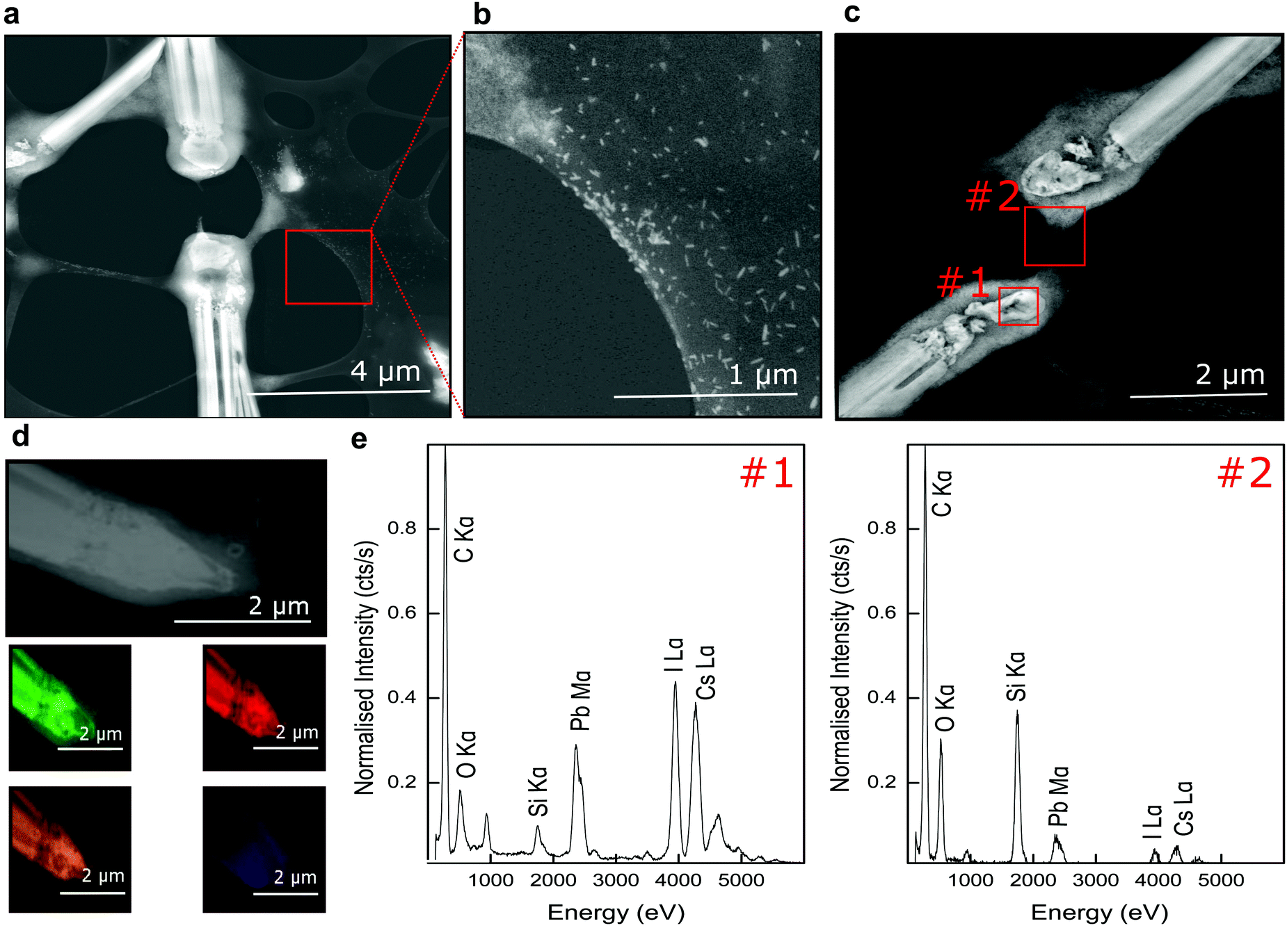 | ||
| Fig. 3 (a) HAADF image of a single microwire which has been cleaved in two by the incident laser. (b) Magnified region of interest showing the formation of number of sub-100 nm particles near the ablation zone. (c) HAADF of a different photoablated microwire. EDX analysis was performed on the two areas highlighted. (d) HAADF of an ablated MW tip (top). The corresponding elemental maps depict Pb Mα (green), I Lα (red), Cs Lα (orange) and C Kα (purple). (e) Normalized EDX spectra from the areas shown in (c). | ||
Elemental composition across the MWs were checked using EDX mapping and HAADF (Fig. 3d and Fig S3, ESI†). Spectral imaging with EDX confirmed spatial overlap of the characteristic Pb Mα, I Lα, Cs Lα X-ray lines predominantly in high contrast areas (Fig. 3d), while the EDX footprint in low contrast, diffuse regions at the ablated tip and surface of the MW was found to largely match that of carbon.
To investigate the waveguide mechanism we follow in the spirit of former publications and study laser-spatio effects on waveguide performance.33 Light intensity mapping (Fig. 4c–h) illustrates the relationship between laser input coordinates and light exiting the MW. Here we employed the 561 nm line and the same MW used in Fig. 1 at a power of <1 kW cm−2. Movement of the laser along the MW axis (Fig. 4d) highlights that small displacements of the input laser coordinates from the tip (Fig. 4c) yields a weak secondary emission site (at around x = 25 μm), along with the transmitted peak at the opposite tip (at x = 16 μm). We postulate this secondary emission effect is due to the termination of the individual smaller NW building blocks at the midway point, as alluded to earlier. Illumination of the MW on the opposite tip (Fig. 4h) displays no evidence of secondary emission lending support to the above model. Further analysis reveals strong waveguide action dominates only when the input laser is directed toward the MW tip (Fig. 4d and h). We suggest that this observation is linked with MW morphology, where facet curving at the microwire tips (Fig. S1, ESI†) demonstrates a quasi-continuum of laser input angles, which supports a slab waveguide model for propagation (Fig. 4b). In comparison the bulk of the MW body lies at a fixed angle normal to the input laser and total internal reflection (TIR) is suppressed in this case (Fig. 4e–g). HAADF imaging of the MWs reveals a hollow cavity spanning the MW length (Fig. 4b), where the input beam is totally internally reflected at the high (n1 = 2.5)34 to low (n2 = 1) refractive index interface at a critical angle of θc = 23°. Employing the attenuation coefficients calculated earlier and the total internal reflection geometry (Fig. 4b), we estimate an average light loss of about 0.8% per reflection when using the 561 nm line. This is comparable to TIR losses of 2% reported per reflection for polymer films.35 At shorter wavelengths we observe greater absorption by the waveguide and consequently greater optical attenuation.
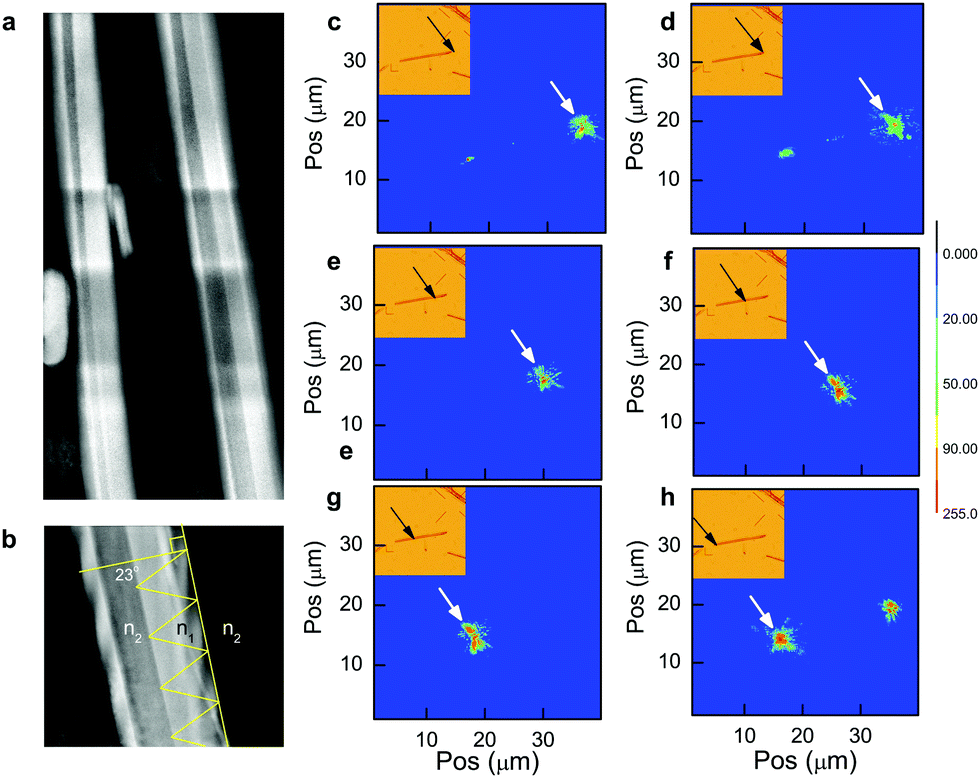 | ||
| Fig. 4 (a) HAADF of two MWs highlighting the low contrast central cavity spanning the MW length. For scale the right hand MW is approx 1000 nm in width (b) Magnified image of the MW, which exhibits a critical angle of θc = 23° and n1 and n2 are the refractive index of the MW (2.5)34 and air (1.0). (c–h) Contour maps of the input 561 nm beam at various microwires sites. The input beam (white arrow) is positioned at x = 36, 35, 30, 28, 19 and 16 μm respectively. The inset shows the brightfield image of the MW and the laser input coordinates indicated by the white arrow. | ||
The emergence of CsPbBr3 MW waveguides has recently come to light and whilst they do share some similarities with our CsPbI3 waveguides the mechanisms governing their behaviour at certain wavelengths appears markedly different. In the case of the CsPbBr3 MWs reported elsewhere,36 above bandgap (2.36 eV) excitation results in PL emission, where the authors indicate a photon recycling mechanism. This was built partly from spectral shifting observations as a function of distance along the MW, as well as former reports on the charging of perovskite surface layers.37 In comparison the CsPbI3 MWs exhibit an optical band gap of 3.04 eV and poorly absorb light above 450 nm, thereby increasing their spectral transmission range relative to the CsPbBr3 reported elsewhere. At shorter wavelengths we detected no spectral shifting which may indicate absence of a photon recycling mechanism but note that the MWs typically underwent ablation before an appreciable PL signal could be produced.
In conclusion CsPbI3 exhibits waveguide properties with increasing efficiencies at longer wavelengths concomitant with a decrease in absorption. The MWs may be dosed with high intensity CW illumination without photoablation when using wavelengths of 532 to 561 nm. Above band-gap excitation leads to a suspected charge-carrier driven redox process and the subsequent formation of lead NPs, while low thermal conductivity results in intense localized heating and the apparent formation of PL active, black phase nanoparticles at the site of photodegradation. At longer wavelengths we employ a slab wave guide model to describe the propagation of light along the MW. HAADF images collected reveal the MWs to be tubular in structure and we propose that the low refractive index of the cavity directs light longitudinally along the high refractive index edges of the MW. It is envisaged that the data reported on CsPbI3 MWs will provide a useful guide to photodamage thresholds in these optical structures and help expedite their translation into functional optical devices.
Author contributions
A. A. E. F. contributed to the manuscript preparation and experimental design. M. A. O. assisted with the development of experimental ideas, data interpretation and manuscript refinement. K. O. R. performed experimental synthesis and photodegradation studies.Funding sources
This work was made possible through the RSC undergraduate research bursary.Conflicts of interest
The authors declare no conflicts of interest.Acknowledgements
The authors would like to thank Giorgio Divitini from the Department of Materials and Metallurgy at the University of Cambridge. We would also like to thank Qiao Chen at the University of Sussex for assisting with SEM analysis and granting access to the XRD instrument.References
- K. Kao and G. A. Hockham, Proc. IEE, 1966, 113, 1151–1158 Search PubMed.
- N. D. Bronstein, Y. Yao, L. Xu, E. O’Brien, A. S. Powers, V. E. Ferry, A. P. Alivisatos and R. G. Nuzzo, ACS Photonics, 2015, 2, 1576–1583 CrossRef CAS.
- L. R. Bradshaw, K. E. Knowles, S. McDowall and D. R. Gamelin, Nano Lett., 2015, 15, 1315–1323 CrossRef CAS PubMed.
- M. G. Debije and P. P. Verbunt, Adv. Energy Mater., 2012, 2, 12–35 CrossRef CAS.
- J. Yoon, L. Li, A. V. Semichaevsky, J. H. Ryu, H. T. Johnson, R. G. Nuzzo and J. A. Rogers, Nat. Commun., 2011, 2, 343 CrossRef PubMed.
- P. T. Lin, V. Singh, J. Hu, K. Richardson, J. D. Musgraves, I. Luzinov, J. Hensley, L. C. Kimerling and A. Agarwal, Lab Chip, 2013, 13, 2161–2166 RSC.
- C. Charlton, M. Giovannini, J. Faist and B. Mizaikoff, Anal. Chem., 2006, 78, 4224–4227 CrossRef CAS PubMed.
- S. Haffouz, K. D. Zeuner, D. Dalacu, P. J. Poole, J. Lapointe, D. Poitras, K. Mnaymneh, X. Wu, M. Couillard and M. Korkusinski, Nano Lett., 2018, 18, 3047–3052 CrossRef CAS PubMed.
- H.-G. Park, C. J. Barrelet, Y. Wu, B. Tian, F. Qian and C. M. Lieber, Nat. Photonics, 2008, 2, 622 CrossRef CAS.
- A. B. Greytak, C. J. Barrelet, Y. Li and C. M. Lieber, Appl. Phys. Lett., 2005, 87, 151103 CrossRef.
- S. Assefa, F. Xia and Y. A. Vlasov, Nature, 2010, 464, 80 CrossRef CAS PubMed.
- Q. Zhang, R. Su, W. Du, X. Liu, L. Zhao, S. T. Ha and Q. Xiong, Small Methods, 2017, 1, 1700163 CrossRef.
- Y. Fu, H. Zhu, C. C. Stoumpos, Q. Ding, J. Wang, M. G. Kanatzidis, X. Zhu and S. Jin, ACS Nano, 2016, 10, 7963–7972 CrossRef CAS PubMed.
- L. N. Quan, J. Kang, C.-Z. Ning and P. Yang, Chem. Rev., 2019, 119, 9153–9169 CrossRef CAS PubMed.
- X. Wang, M. Shoaib, X. Wang, X. Zhang, M. He, Z. Luo, W. Zheng, H. Li, T. Yang and X. Zhu, ACS Nano, 2018, 12, 6170–6178 CrossRef CAS PubMed.
- K. Park, J. W. Lee, J. D. Kim, N. S. Han, D. M. Jang, S. Jeong, J. Park and J. K. Song, J. Phys. Chem. Lett., 2016, 7, 3703–3710 CrossRef CAS PubMed.
- S. W. Eaton, M. Lai, N. A. Gibson, A. B. Wong, L. Dou, J. Ma, L.-W. Wang, S. R. Leone and P. Yang, Proc. Natl. Acad. Sci. U. S. A., 2016, 113, 1993–1998 CrossRef CAS PubMed.
- L. Protesescu, S. Yakunin, M. I. Bodnarchuk, F. Krieg, R. Caputo, C. H. Hendon, R. X. Yang, A. Walsh and M. V. Kovalenko, Nano Lett., 2015, 15, 3692–3696 CrossRef CAS PubMed.
- B. Zhao, S.-F. Jin, S. Huang, N. Liu, J.-Y. Ma, D.-J. Xue, Q. Han, J. Ding, Q.-Q. Ge and Y. Feng, J. Am. Chem. Soc., 2018, 140, 11716–11725 CrossRef CAS PubMed.
- A. Swarnkar, A. R. Marshall, E. M. Sanehira, B. D. Chernomordik, D. T. Moore, J. A. Christians, T. Chakrabarti and J. M. Luther, Science, 2016, 354, 92–95 CrossRef CAS PubMed.
- Z. Wang, J. Liu, Z.-Q. Xu, Y. Xue, L. Jiang, J. Song, F. Huang, Y. Wang, Y. L. Zhong, Y. Zhang, Y.-B. Cheng and Q. Bao, Nanoscale, 2016, 8, 6258–6264 RSC.
- F. Zhao, C. Liu, Y. Sun, Q. Li, J. Zhao, Z. Li, B. Zhang, C. Lu, Q. Li, S. Qiao and Y. S. Zhao, Org. Electron., 2019, 74, 276–281 CrossRef CAS.
- C. C. Boyd, R. Cheacharoen, T. Leijtens and M. D. McGehee, Chem. Rev., 2018, 119, 3418–3451 CrossRef PubMed.
- N. F. Mott, Sir Nevill Mott: 65 years in physics, World Scientific, 1995 Search PubMed.
- B. Wang, N. Novendra and A. Navrotsky, J. Am. Chem. Soc., 2019, 141, 14501–14504 CrossRef CAS PubMed.
- S. Dastidar, C. J. Hawley, A. D. Dillon, A. D. Gutierrez-Perez, J. E. Spanier and A. T. Fafarman, J. Phys. Chem. Lett., 2017, 8, 1278–1282 CrossRef CAS PubMed.
- M. S. Kirschner, B. T. Diroll, P. Guo, S. M. Harvey, W. Helweh, N. C. Flanders, A. Brumberg, N. E. Watkins, A. A. Leonard and A. M. Evans, Nat. Commun., 2019, 10, 504 CrossRef CAS PubMed.
- K. Miyata, D. Meggiolaro, M. T. Trinh, P. P. Joshi, E. Mosconi, S. C. Jones, F. De Angelis and X.-Y. Zhu, Sci. Adv., 2017, 3, e1701217 CrossRef PubMed.
- J. Yang, X. Wen, H. Xia, R. Sheng, Q. Ma, J. Kim, P. Tapping, T. Harada, T. W. Kee and F. Huang, Nat. Commun., 2017, 8, 14120 CrossRef CAS PubMed.
- G. Yuan, C. Ritchie, M. Ritter, S. Murphy, D. E. Gómez and P. Mulvaney, J. Phys. Chem. C, 2018, 122, 13407–13415 CrossRef CAS.
- A. K. Jena, A. Kulkarni, Y. Sanehira, M. Ikegami and T. Miyasaka, Chem. Mater., 2018, 30, 6668–6674 CrossRef CAS.
- C. Bi, S. V. Kershaw, A. L. Rogach and J. Tian, Adv. Funct. Mater., 2019, 29, 1902446 CrossRef.
- P. Guo, X. Shen, B. Zhang, H. Sun, Z. Zou, W. Yang, K. Gong and Y. Luo, Nanotechnology, 2018, 29, 185201 CrossRef PubMed.
- M. Ahmad, G. Rehman, L. Ali, M. Shafiq, R. Iqbal, R. Ahmad, T. Khan, S. Jalali-Asadabadi, M. Maqbool and I. Ahmad, J. Alloys Compd., 2017, 705, 828–839 CrossRef CAS.
- W. R. L. Thomas, J. M. Drake and M. L. Lesiecki, Appl. Opt., 1983, 22, 3440–3450 CrossRef CAS PubMed.
- I. Dursun, Y. Zheng, T. Guo, M. De Bastiani, B. Turedi, L. Sinatra, M. A. Haque, B. Sun, A. A. Zhumekenov, M. I. Saidaminov, F. P. García de Arquer, E. H. Sargent, T. Wu, Y. N. Gartstein, O. M. Bakr, O. F. Mohammed and A. V. Malko, ACS Energy Lett., 2018, 3, 1492–1498 CrossRef CAS.
- S. P. Sarmah, V. M. Burlakov, E. Yengel, B. Murali, E. Alarousu, A. M. El-Zohry, C. Yang, M. S. Alias, A. A. Zhumekenov, M. I. Saidaminov, N. Cho, N. Wehbe, S. Mitra, I. Ajia, S. Dey, A. E. Mansour, M. Abdelsamie, A. Amassian, I. S. Roqan, B. S. Ooi, A. Goriely, O. M. Bakr and O. F. Mohammed, Nano Lett., 2017, 17, 2021–2027 CrossRef CAS PubMed.
Footnote |
| † Electronic supplementary information (ESI) available: Materials and methods, Fig. S1–S3 (PDF), supplementary Video S1 (avi), supplementary Video S2 (avi). See DOI: 10.1039/d0ma00043d |
| This journal is © The Royal Society of Chemistry 2020 |