
 Open Access Article
 This Open Access Article is licensed under a
 Creative Commons Attribution 3.0 Unported Licence
Role of the electronically-active amorphous state in low-temperature processed In2O3 thin-film transistors†
Ahmad R.
Kirmani‡
 ,
Emily F.
Roe‡
,
Christopher M.
Stafford
and
Lee J.
Richter
*
,
Emily F.
Roe‡
,
Christopher M.
Stafford
and
Lee J.
Richter
*
Materials Science and Engineering Division, National Institute of Standards and Technology (NIST), Gaithersburg, MD 20899, USA. E-mail: lee.richter@nist.gov
First published on 4th April 2020
Abstract
Metal oxide (MO) thin-film transistors (TFTs) are expected to enable low-cost flexible and printed electronics, given their excellent charge transport, low processing temperatures and solution processability. However, achieving adequate mobility when processed scalably at low temperatures compatible with plastic electronics is a challenge. Here, we explore process-structure-transport relationships in blade-coated indium oxide (In2O3) TFTs via both sol–gel and combustion chemistries. We find that the sol–gel chemistry enables n-type TFTs when annealed at 200 °C to 225 °C with noticeable electron mobility ((3.4 ± 0.4) cm2 V−1 s−1) yet minimal In2O3 crystallinity and surprisingly low levels of the metal–oxygen–metal (M–O–M) lattice content (≈46%). Increased annealing temperatures result in the appearance of nanocrystalline domains and an increase in M–O–M content to ≈70%, without any further increase in mobility. An acetylacetone combustion-assisted ink lowers the external thermal budget required for In2O3 crystallization but bypasses the electronically-active amorphous state and underperforms the sol–gel ink at low temperatures. Grain boundary formation and nanocrystalline inclusions in these films due to rapid combustion-assisted crystallization are suggested to be the likely origin behind the significantly compromised charge transport at low-temperatures. Overall, this study emphasizes the need to understand the complex interplay between local order (nanocrystallinity) and connectivity (grain boundary, amorphous phases) when optimizing low-temperature processed MO thin films.
Introduction
Metal oxides (MOs) have been extensively explored for wide-ranging applications in flexible electronics, optoelectronics and biosensing.1–3 Thin films of these MOs can be produced from solution-based inks, enabling low-cost, large-area printing of next-generation thin-film semiconducting devices. Given their wide bandgaps (≈3.0 eV), these materials promise fabrication of transparent electronics.4,5 A major reason behind the interest in these materials is their ability to conduct charges even when their crystal lattices are in a disordered, amorphous state.4 Unlike silicon, where a transition from crystalline to the amorphous state is accompanied with a significant depreciation in charge transport due to the directionality of sp3 orbitals, ns orbitals of the transition metal form the MO conduction band.4,6 Being spherical and isotropic, these orbitals enable charge transport that is not substantially affected by disorder in the amorphous state. Since the amorphous state requires lower annealing temperatures compared to the crystalline state, amorphous MOs are naturally more compatible with flexible electronics.Amongst MOs, indium oxide (In2O3) has garnered significant attention owing to its excellent carrier mobilities and ease of fabrication. In 2004, a facile route to flexible MO thin-film transistors (TFTs) was demonstrated, which sparked great interest in finding solution-processable alternatives to amorphous silicon.4 In general, sol–gel processed thin films cast from an ink of an indium precursor dissolved in a polar solvent, such as water or 2-methoxyethanol (MeOEt), are annealed at an elevated temperature resulting in conversion to In2O3.1,7–11 These efforts have allowed fabrication of high field-effect mobility n-type In2O3 TFTs (ca. 10 cm2 V−1 s−1) at annealing temperatures in the range of 300 °C to 400 °C via a condensation reaction that converts the indium precursor to the oxide.1,12–15 With an aim of reducing the thermal budget, combustion synthesis has been recently introduced, targeting both TFT and electron transport layer applications.11,16,17 Aided by a fuel that is mixed with the precursor solution, the processing temperature required for In2O3 conversion is reduced. The resulting exothermic reaction has been found to reduce the oxide conversion temperature to ca. 250 °C to 300 °C.11,16 In2O3 and other technologically relevant MO-TFTs have been explored using blade-coating and spray coating.5,9,10,18,19 Recently, combustion blade coating has been demonstrated to reduce film-processing time and improve industrial compatiblity.9 In2O3 is a particularly interesting system for fundamental study as, unlike in the common InGaZnO quaternary system, both crystalline and amorphous films can be realized. Amorphous oxide phases should confer advantages in flexible applications. Recent studies have employed organic and inorganic additives to intentionally frustrate crystallization.7,11,20,21 However, fundamental studies aimed at the low-temperature processed amorphous phase in solution-deposited In2O3 TFTs are limited,22,23 and therefore needed.
In this study, we explore blade-coating of In2O3 films using both sol–gel and acetylacetone combustion synthesis-based inks. We observe that the sol–gel chemistry allows fabrication of electrically-active amorphous In2O3 TFTs at process temperatures as low as 200 °C, with electron mobilities approaching 1 cm2 V−1 s−1 (max. 4.6 cm2 V−1 s−1 at 212 °C). Notably, these films are found to feature only ≈45% of the metal–oxygen–metal (M–O–M) lattice content, suggesting minimal formation of the oxide matrix is adequate for charge carrier percolation pathways. Surprisingly, devices fabricated via the acetylacetone combustion synthesis ink underperform those from the sol–gel. X-ray scattering indicates the combustion-processed films crystallize at lower processing temperatures and bypass the electronically-active amorphous state.
Results and discussion
Sol–gel (hereafter, sg-) ink was produced by dissolving indium nitrate hydrate (In(NO3)3·xH2O) precursor in MeOEt followed by vigorous mixing over several hours. To enable blade-coated films from the ink, coating conditions were first optimized. Blade coating is a meniscus-guided large-area compatible coating technique and is similar in principle to slot-die coating, an established technique for upscaling film coating.24,25 We note that it was not possible to blade-coat these inks uniformly at room temperature due to a de-wetting instability of the ink which resulted in non-uniformities (thickness gradients) and pin-holes (Fig. S1, ESI†). Optimization of the substrate temperature appropriately tuned the ink surface tension and resulted in highly uniform films at 60 °C. The high quality of these films is reflected in the observation of clear thin-film interference features along qz, due to X-rays forming standing waves within the well-defined top- and bottom-interfaces of the films during X-ray scattering (Fig. S2, ESI†). All films reported were coated at 5 mm s−1. Freshly-coated sg-In2O3 films were ≈28 nm thick and shrank to ≈8 nm upon annealing resulting in a ≈72% volume contraction, as determined by spectroscopic ellipsometry (SE). Characterization of the thickness dependence on the coating speed (Fig. S3, ESI†) indicates the films were deposited in the Landau–Levich–Derjaguin regime.26,27Fig. 1 depicts the various steps involved in fabrication of blade-coated sg-In2O3 TFTs for this study. Photographs of the initial precursor solution and the final device are included in the inset. As shall be discussed later, the same protocol was followed for combustion (hereafter, c-) In2O3 TFTs, with the only difference being the composition of the initial precursor solution. Freshly-coated c-In2O3 films were ≈47 nm thick and shrank to ≈8 nm upon annealing resulting in a ≈83% volume contraction, noticeably more than the corresponding sg-In2O3 films. 10 μL of the filtered precursor solution was introduced into the blade-substrate gap (ca. 200 μm), with the cleaned 230 nm SiO2/Si substrate maintained at 60 °C. The blade was subsequently translated at 5 mm s−1 using a programmed translating stage along the substrate length. As the meniscus front moved with the blade, the ink was pushed out of the gap and deposited on the substrate in the form of a thin film. Care must be taken to immediately initiate the blade translation after the ink comes in contact with the heated substrate. The coated film was then annealed at a specific temperature for 15 min. Annealing densified the film and led to formation of an M–O–M framework. Due to the significant volume change upon annealing, film porosity may develop. Prior reports have typically deposited channels via multiple (2 to 4) coating cycles, in an effort to fill in pores and minimize cracks.7,9 In this study we used two coats for every device condition resulting in ≈16 nm thick channels. Atomic force microscopy (AFM) data on sg-In2O3 films shows a slightly reduced surface roughness after two coats compared to a single coat (Fig. S4, ESI†). Our AFM lateral resolution is limited to ≈10 nm and nanoscopic features/grains below this size regime cannot be resolved.
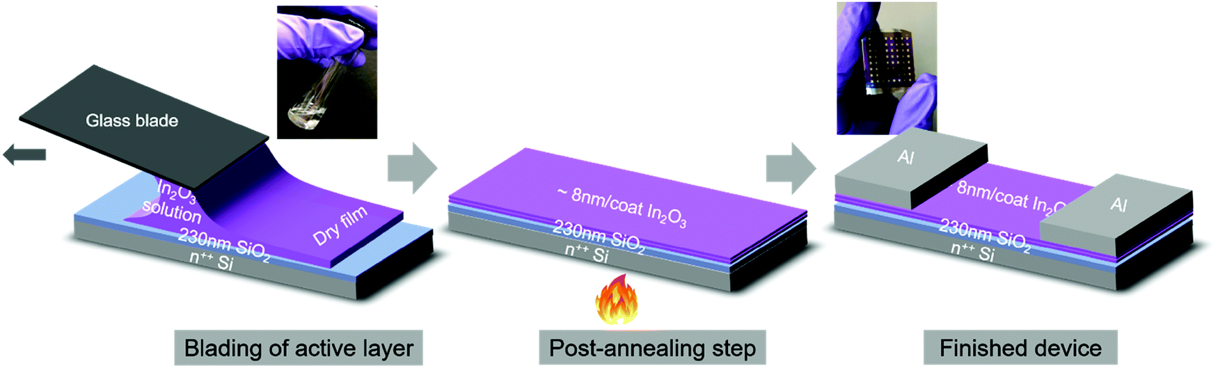 | ||
| Fig. 1 Schematic representation of the various stages involved in blade-coating of In2O3 TFTs. | ||
Fig. 2a and b show representative transfer curves for the bladed sg- and c-In2O3 devices. Minimal hysteresis was found in the transfer curves, which was independent of the annealing temperature (Fig. S5, ESI†). Output curves for a representative device for each temperature condition are shown in Fig. S6 (ESI†). ION/IOFF ratio for temperatures >225 °C are in the range of 106. Dependence of saturation mobility (μsat) on annealing temperature is shown in Fig. 2c and d. sg-In2O3 TFTs achieve reasonable electron mobilities at annealing temperatures as low as 200 °C (with peak μsat at 212 °C = 4.6 cm2 V−1 s−1, Fig. S7, ESI†). Mean mobility shows an increase up to 225 °C beyond which it nominally saturates at ≈(2 to 4) cm2 V−1 s−1. These values are in line with previous reports that have employed spin-coating,7,11,14 and a recent report of blade-coating.9 In contrast, c-In2O3 TFTs show a monotonic mobility trend wherein the mobilities keep increasing with annealing temperature. Surprisingly, in this case, mobilities are lower than sg-In2O3 TFTs, specially at low temperatures (200 °C to 250 °C). For high temperatures (325 °C), μsat is ≈ 2 cm2 V−1 s−1. VTH are shown in Fig. 2e and f and are negative for high-mobility (high temperature) TFTs. The dependence of VTH on annealing temperature is similar for both sg- and c-In2O3. Generally, highly negative VTH in In2O3 has been linked to an overabundance of oxygen vacancies in the oxide which behave as electron donors and result in a large bulk electron concentration.28,29 Device parameters are summarized in Table 1.
 | ||
| Fig. 2 Representative transfer curves for (a) sg-In2O3, and (b) c-In2O3 TFTs for various annealing temperatures (VDS = 40 V). Saturation mobilities (μsat) and threshold voltages (VTH) for 10 to 20 devices per condition are shown for sg- (c and e) and c-In2O3 TFTs (d and f). Boxes represent the 1st and 3rd quartiles of data, whiskers denote the highest/lowest datapoint, dashes represent medians, solid circles denote the means. | ||
| T (°C) | μ sat (cm2 V−1 s−1) | V TH (V) | log10(ION/IOFF) | |||
|---|---|---|---|---|---|---|
| Sol–gel | Combustion | Sol–gel | Combustion | Sol–gel | Combustion | |
| 200 | 0.7 ± 0.2 (2.3) | 0.007 ± 0.0 (0.04) | 15.5 ± 6.5 | 20.5 ± 6.1 | 6.2 ± 0.3 | 3.8 ± 0.2 |
| 225 | 3.4 ± 0.4 (6.0) | 0.09 ± 0.02 (0.18) | −23.7 ± 2.2 | −20.3 ± 5.2 | 5.8 ± 0.4 | 3.6 ± 0.2 |
| 250 | 4.2 ± 0.2 (6.7) | 0.6 ± 0.1 (1.2) | −23.0 ± 3.1 | −12.0 ± 3.0 | 5.8 ± 0.2 | 5.3 ± 0.3 |
| 275 | 1.9 ± 0.3 (3.6) | 1.2 ± 0.1 (1.4) | −22.3 ± 2.3 | −14.6 ± 1.7 | 4.9 ± 0.2 | 5.7 ± 0.2 |
| 300 | 2.7 ± 0.3 (4.2) | 1.0 ± 0.0 (1.1) | −17.9 ± 3.6 | −4.3 ± 3.3 | 5.0 ± 0.1 | 5.5 ± 0.1 |
| 325 | 3.3 ± 0.4 (6.3) | 2.1 ± 0.1 (2.5) | −18.6 ± 3.5 | −38.2 ± 2.1 | 4.5 ± 0.1 | 4.8 ± 0.1 |
To understand and explain these charge transport trends, we carried out studies of chemical composition, crystallinity and nanoscale structure. X-ray photoelectron spectroscopy (XPS) measurements were performed on the oxygen (O) 1s, indium (In) 3d5/2, carbon (C) 1s and nitrogen (N) 1s core levels for sg- and c-In2O3 annealed at 225 °C and 325 °C. ≈20% C and ≈1% N were found in all the samples, irrespective of the annealing temperature, in agreement with earlier findings.30 The significant amount of C in the films is likely due to residual solvent and/or solvent decomposition fragments. The O1s core level peak contains information about the various chemical environments of oxygen in the matrix, such as hydroxylated oxygen (M–OH), oxygen bonded to organic functionalities (M–OR) and lattice oxygen (M–O–M), all appearing at slightly different binding energies (BE).8,11,16,19 The latter component, M–O–M, belongs to the oxide network and increases with oxide formation. Fig. 3a shows the O1s core peak for 225 °C and 325 °C annealed sg- and c-In2O3 films. These films are ≈16 nm thick and are blade-coated following the TFT fabrication protocol to mimic device-relevant channel conditions. All the peaks are referenced to the 285.0 eV amorphous component of C1s.
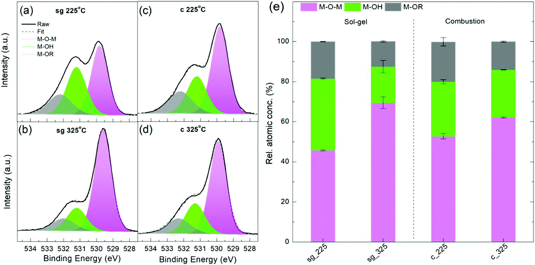 | ||
| Fig. 3 (a–d) High-resolution XPS O1s core level peaks. The peaks are deconvoluted into M–O–M (pink), M–OH (green) and M–OR (grey) components. Intensity is normalized to the overall peak area. (e) Relative concentrations of the M–O–M, M–OH and M–OR components of the O1s peaks shown in (a–d), averaged over 3 spots. Error bars represent ± one standard deviation of the mean. | ||
The peaks were deconvoluted into three components: M–O–M species (pink, centered at (529.8 ± 0.1) eV), M–OH species (green, centered at (531.2 ± 0.1) eV) and M–OR species (grey, centered at (532.2 ± 0.1) eV), as widely reported in literature.5,7,9,11,16–18,31–33 An alternate assignment of the (531.2 ± 0.1) eV component considers it to be arising from oxygen atoms present next to oxygen vacancies (VO).1,28,30 Choice of the assignment does not change the peak fit and conclusions drawn. In the current study, we have considered the (531.2 ± 0.1) eV component to be M–OH, and not VO. As annealing temperature is increased to 325 °C, this component is slightly suppressed for both sg- and c-films (Fig. 3e), as would be expected for –OH species.
From Fig. 3 and Table 2 it is clear that, for both sg- and c-In2O3, increasing the annealing temperature from 225 °C to 325 °C increases the M–O–M content, while suppressing the M–OH and M–OR species. Fig. S8 (ESI†) shows In 3d5/2 core level peaks for the various conditions. Fitted In 3d5/2 peak components are shown in Table S1 (ESI†).30 The component corresponding to the M–O–M lattice content is found to increase with temperature, accompanied with a reduction in metallic In, M–OH and M–OR species, in agreement with O1s trends.
| Sample | M–O–M | M–OH | M–OR |
|---|---|---|---|
| sg 225 °C | 45.8 ± 0.3 | 35.7 ± 0.3 | 18.5 ± 0.1 |
| sg 325 °C | 69.6 ± 1.3 | 17.9 ± 1.0 | 12.6 ± 2.3 |
| c 225 °C | 52.8 ± 1.4 | 27.2 ± 1.0 | 19.9 ± 2.1 |
| c 325 °C | 62.2 ± 0.3 | 23.7 ± 0.1 | 14.1 ± 0.3 |
It is important to note that XPS is a highly surface-sensitive characterization tool and does not probe more than the top ≈10 nm of the film. The films considered in the above analysis were 16 nm thick and the entire thickness, specially the bottom, is crucial when these are used as the channel layer in bottom-gate-top-contact TFT configuration. Although Ar+ depth profiling is a viable route to probe chemical composition and oxidation states deep inside the film, the destructive nature of the process can result in undesirable chemical modifications. To test for vertical gradients in the oxygen state, we repeated the XPS measurements on thinner (8 nm) films. Data is shown in Fig. S9 and S10 (Tables S2 and S3) (ESI†) and the findings are similar to the 16 nm films. Fig. S11 and Table S4 (ESI†) show the relative concentrations of O, In, C and N for all the samples.
Fig. 4 shows the 2D grazing-incidence wide-angle X-ray scattering (GIWAXS) patterns for sg- and c-In2O3 films and corresponding sector-averages. These films were fabricated following the same protocol as the corresponding TFTs to mimic channel fabrication conditions. For T = 200 °C and 225 °C, a weak amorphous halo around 2.2 Å−1 is visible for sg-In2O3, pointing toward the amorphous nature of this film. At higher temperatures, several well-defined Bragg diffraction rings emerge as the films become crystalline. The strongest peak is at 2.22 Å−1 corresponding to the (222) plane of the cubic oxide phase.34,35 The crystallites are randomly oriented and lack texture. Noticeable diffuse spots in the 2D patterns are the diffuse scattering from the silicon (substrate). For the case of c-In2O3, well-defined features are observed for all temperatures in the range of 200 °C to 350 °C. This suggests that, as expected, the added fuel lowers the process temperature required for crystallization and indicates the film bypasses the low-temperature amorphous phase observed for sg-In2O3.
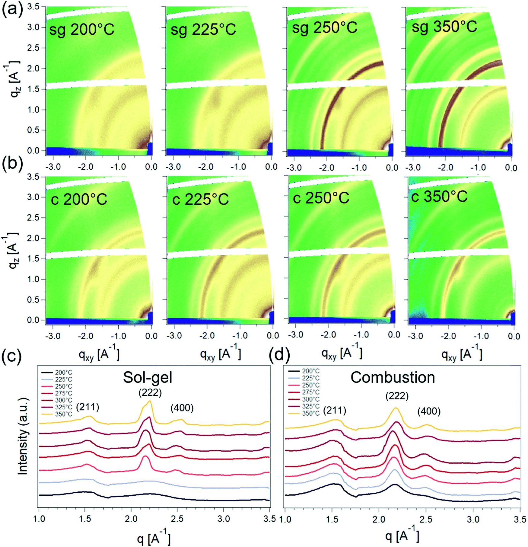 | ||
| Fig. 4 (a) and (b) 2D GIWAXS patterns for T = 200 °C, 225 °C, 250 °C and 350 °C sg- and c-In2O3 films. White bars are detector blind spots. Corresponding sector averages over all azimuthal angles in the range of 0° to 90° are shown in (c) and (d), respectively. | ||
Grazing-incidence small-angle X-ray scattering (GISAXS) was next used to probe the nature of the crystallinity evolution seen in GIWAXS. GISAXS probes the local electronic density contrast at the nanoscale and has been the technique of choice for understanding formation and self-assembly of colloidal nanocrystals.36,37 2D GISAXS patterns and the corresponding horizontal line-averages of the Yoneda enhanced scattering for sg- and c-In2O3 are shown in Fig. 5. sg-In2O3 films do not show any significant scattering contrast for T = 200 °C and 225 °C. Contrary to this, c-In2O3 exhibits scattering intensity corresponding to formation of lateral domains for temperatures as low as T = 200 °C. Based on correlation between the scattering and the crystallinity reflected in GIWAXS we attribute the coherence peaks (Fig. 5c and d) to the lateral separation between nanocrystalline domains. The nature of the low-density phase (amorphous In2O3, void, etc.) cannot be determined. Analysis of these patterns allows us to estimate the evolution of this distance with temperature. As the temperature increases, the amorphous phase begins to crystallize and In2O3 nanodomains ripen. For sg-In2O3, domains do not develop until T = 250 °C. In contrast, for c-In2O3 an inter-domain distance of ≈7.0 nm is found at T = 200 °C, which increases slowly to ≈8.0 nm for T = 350 °C.
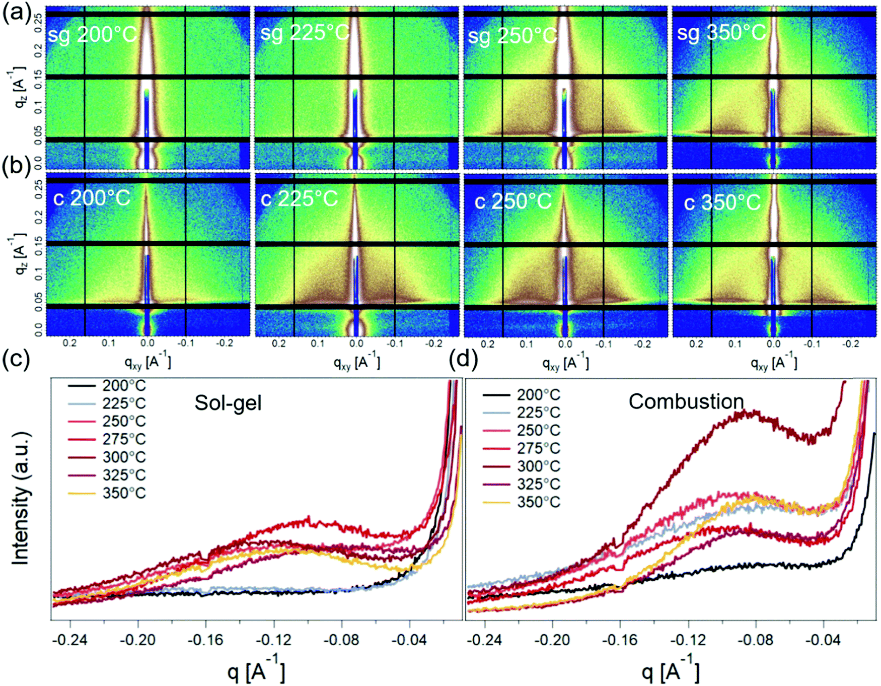 | ||
| Fig. 5 (a)–(c) 2D GISAXS patterns for T = 200 °C, 225 °C, 250 °C and 350 °C sg- and c-In2O3 films. Black bars are detector blind spots. Corresponding horizontal line-averages are shown in (c) and (d), respectively. | ||
From the combined X-ray scattering and XPS results, a consistent picture of the film structure emerges that can be correlated to the TFT performance. These results reveal the crystallization of sg- and c-In2O3 and its impact on charge transport. Complete conversion of the as-cast film to the oxide phase has not taken place at 225 °C, with a large fraction being comprised of M–OH and M–OR. The surprising observation of appreciable charge transport at these low temperatures for sg-In2O3, therefore, implies the presence of a sufficiently percolative network of the converting oxide network to enable flow of electrons. sg-In2O3 TFTs are in an electronically-active amorphous state at these temperatures. This result is in line with recent reports where the amorphous state with appreciable charge transport has been achieved by deliberately introducing additives to frustrate In2O3 crystallization.7,11,20 Further increase in annealing temperature results in formation of nanoscale domains along with an increase in (222) peak intensity suggesting onset of oxide crystallization. This happens at 250 °C for sg-In2O3. At 325 °C, these films show a marked increase in M–O–M content and appearance of (211), (222) and (400) peaks signaling oxide crystallization. However, no improvement in charge transport upon crystallization is observed for these sg-In2O3 films.
c-In2O3 exhibits a contrasting process-structure-transport behavior. At lower temperatures, these TFTs are found to significantly underperform sg-In2O3. Yet GIWAXS indicates that crystalline domains have formed at temperatures as low as 225 °C. These observations are consistent with the expectation that the combustion ink will enable oxide conversion at lower annealing temperatures. c-In2O3 films, therefore, appear to bypass the low-temperature amorphous state. It is likely that charge transport in these 200 °C to 250 °C annealed blade-coated films is limited by grain boundaries due to the more rapid combustion aided crystallization due to acetylacetone. In fact, enhanced scattering intensity in GISAXS at these low temperatures strongly points toward presence of internal porosity and grain boundaries. Also, as discussed earlier, the as-prepared combustion film undergoes significant volume contraction (83%) upon annealing and conversion to c-In2O3. This can potentially lead to increased porosity and poorer grain connectivity. Moreover, it has been suggested that nanocrystalline domains in the early stages of crystallization can act as charge carrier traps limiting μsat, which might additionally explain the poor charge transport observed in these low-temperature processed c-In2O3 TFTs.22 More abrupt grain boundaries in c-In2O3 films vs. sg-In2O3 films is consistent with the overall increased GISAXS signal in Fig. 5. Further increase in annealing temperature and M–O–M lattice content possibly creates percolation pathways for charge carriers and strikes a trade-off with poor grain connectivity. As a result, μsat increases monotonically and reaches ≈2 cm2 V−1 s−1 at 325 °C.9
Conclusions
In summary, we have explored low-temperature processing of blade-coated In2O3 TFTs comparing sol–gel and acetylacetone-based combustion ink chemistries. We find the oxide crystallization behaviors via the two processing routes to be very contrasting. We track the M–O–M content and crystallization with annealing temperature and observe that sol–gel ink allows fabrication of electronically-active amorphous TFT channels with noticeable charge transport (μsat ≈ 3 cm2 V−1 s−1) at temperatures as low as 200 °C to 225 °C. Increase in annealing temperature results in a higher M–O–M content, an intense and well-defined (222) crystallographic peak and presence of nanocrystalline domains, all pointing to conversion of the amorphous film into crystalline oxide. However, μsat is found to remain relatively unchanged as temperature is increased and is independent of crystallization. c-In2O3 films bypass the initial electronically-active amorphous phase, consistent with the latent heat of the combustion reaction. Charge transport in these films during early stages of crystallization at low temperatures, however, is inhibited possibly due to grain growth and nano-inclusions that act as charge traps. μsat lags behind for low-temperatures (200 °C to 250 °C), and increases to ≈2 cm2 V−1 s−1 at 325 °C. It should be noted that our results regarding the combustion chemistry relate only to acetylacetone-fuel based combustion synthesis and should not be generalized to other fuels, such as, urea and glucose. This work demonstrates the subtle interplay between structural motifs: amorphous vs. crystalline and defects: nanocrystalline boundaries, etc. that must be navigated when optimizing ink formulation and coating conditions. Leveraging the electrically active amorphous state, we achieve low-temperature In2O3 TFTs with reasonable charge transport, directly compatible with flexible electronics.Experimental section
Synthesis of In2O3 precursor inks
For sg-In2O3, 284 mg In(NO3)3·xH2O precursor was dissolved in 2 mL MeOEt at room temperature in air to form an ink concentration of 0.4 mol L−1. The solution was vigorously stirred at room temperature (≈22 °C) in ambient atmosphere for at least 12 h. For c-In2O3, 200 μL acetylacetone (fuel) and 100 μL NH4OH were also added to the above 0.4 mol L−1 solution, followed by vigorous stirring at room temperature for at least 12 h. In(NO3)3·xH2O precursor was purchased from Alfa Aeser. (Certain commercial equipment, instruments, or materials are identified in this paper in order to specify the experimental procedure adequately. Such identification is not intended to imply recommendation or endorsement by the National Institute of Standards and Technology, nor is it intended to imply that the materials or equipment identified are necessarily the best available for the purpose.) All the other chemicals were purchased from Sigma Aldrich. In(NO3)3·xH2O precursor from Sigma Aldrich was also used in this study to confirm reproducibility.Device fabrication and testing
p-Doped silicon (resistivity = 0.001–0.005 Ohm cm) with 230 nm thermal SiO2 were used for the bottom gate devices. Thickness of the thermal oxide was determined using ellipsometry. Substrates were ultrasonically cleaned sequentially with acetone and isopropanol, for 15 min each. The substrates were then exposed to ultraviolet-ozone treatment (UVO) for 10 min prior to blade coating. After coating, the chips were placed on a hot plate set at the target temperature for 15 min. Two such coating cycles were performed for all the devices and X-ray scattering measurements reported in this study. All coatings and annealing steps were performed in ambient atmosphere with uncontrolled relative humidity. 35 nm of aluminum (Al) was thermally deposited as the top electrode, such that the channels had a width of 1000 μm and length of either 100 μm or 50 μm. Transfer curves were measured using a semiconductor parameter analyzer in saturation regime (VDS = 40 V). A linear fit to the square root of drain current (in VGS range of 30 V–40 V) was used to extract μsat and VTH.Blade coating of In2O3 inks
A cleaned substrate was placed on the blade coater stage maintained at 60 °C and held firm with vacuum. A clean glass slide (blade) was mounted to the setup and brought to a height of 200 μm from the substrate using a custom-made laser setup.38 Precursor solution was filtered with a 0.45 μm filter. 10 μL of the solution was introduced into the blade-substrate gap and the blade was translated across the substrate using a programmed translator at 5 mm s−1. Coating was done in ambient atmosphere.X-ray scattering measurements
Samples were blade coated on 230 nm SiO2/Si substrates using the same protocol as used for TFTs. For GIWAXS, measurements were done at a detector distance of 0.153 m while a distance of 2.789 m was used for GISAXS. Samples were measured using X-ray wavelength of 0.826 Å at 0.20° angle of incidence with respect to the substrate plane. Scattering intensity was detected by a PILATUS 300 K detector (GIWAXS) and a PILATUS 2M detector (GISAXS). Nika software package was used to sector average the 2D GIWAXS and GISAXS images. Data plotting was done in Igor Pro (Wavemetrics, Inc., Lake Oswego, OR, USA).Spectroscopic ellipsometry
An M-2000XI, J. A. Woollam Co., Inc. ellipsometer (210 nm to 1700 nm) was used to measure the film thicknesses and complex refractive indices. The spectra were obtained at incidence angles in the range 49° to 70° with discrete increments of 7°. The film properties were modelled assuming a Cauchy dispersion relation in the optically transparent region using the CompleteEASE software from J. A. Woollam Co., Inc.X-ray photoelectron spectroscopy (XPS)
XPS measurements were performed using a Kratos AXIS Ultra DLD Spectrometer (Kratos Analytical) with a monochromatic Al Kα source (1486.6 eV) operating at 140 W. The base pressure of the sample analysis chamber was ≈1.0 × 10⁻⁹ Torr (or 1.33 × 10⁻⁷ Pa), and spectra were collected from a nominal spot size of 300 μm × 700 μm and a take-off angle of 90° (normal to the surface). Measurements were performed in hybrid mode using electrostatic and magnetic lenses, and the pass energy of the analyzer was set at 160 eV for survey scans and 20 eV for high resolution scans, with energy resolutions of 0.5 eV and 0.1 eV. All XPS data analysis was performed using the CasaXPS software package.Atomic force microscopy
AFM images were collected using a Dimension Icon operating in tapping mode. Silicon probes (TAP525A, Bruker Nano Surfaces) with a nominal spring constant of 200 N m−1 and resonant frequency of 525 kHz were used to image the films. AFM images were collected over a (5 × 5) μm2 area at a scan rate of 0.754 Hz. The images were analyzed using the NanoScope Analysis software. RMS roughness was determined using the roughness function within the NanoScope analysis software after applying a 1st order flattening function.Conflicts of interest
There are no conflicts to declare.Acknowledgements
EFR acknowledges support from the National Institute of Standards and Technology (NIST) SURF Fellowship Program. X-ray scattering measurements were carried out at the CMS beamline of the National Synchrotron Light Source II (NSLS II), a U.S. Department of Energy (DOE) Office of the Science User Facility operated for the DOE Office of Science by Brookhaven National Laboratory under Contract No. DE-SC0012704. ARK and LJR thank Dr Ruipeng Li and Dr Masafumi Fukuto for their assistance with X-ray scattering measurements at NSLS II, Dr Emily G. Bittle for helpful discussions regarding device characterization, and Dr Binghao Wang for helpful insights into combustion oxide inks.References
- K. K. Banger, Y. Yamashita, K. Mori, R. L. Peterson, T. Leedham, J. Rickard and H. Sirringhaus, Low-temperature, high-performance solution-processed metal oxide thin-film transistors formed by a ‘sol–gel on chip’ process, Nat. Mater., 2010, 10, 45 CrossRef PubMed.
- N. Nakatsuka, K.-A. Yang, J. M. Abendroth, K. M. Cheung, X. Xu, H. Yang, C. Zhao, B. Zhu, Y. S. Rim and Y. Yang, et al., Aptamer–field-effect transistors overcome Debye length limitations for small-molecule sensing, Science, 2018, 362(6412), 319–324 CrossRef CAS PubMed.
- X. Yu, T. J. Marks and A. Facchetti, Metal oxides for optoelectronic applications, Nat. Mater., 2016, 15, 383 CrossRef CAS.
- K. Nomura, H. Ohta, A. Takagi, T. Kamiya, M. Hirano and H. Hosono, Room-temperature fabrication of transparent flexible thin-film transistors using amorphous oxide semiconductors, Nature, 2004, 432(7016), 488–492 CrossRef CAS PubMed.
- B. Wang, X. Yu, P. Guo, W. Huang, L. Zeng, N. Zhou, L. Chi, M. J. Bedzyk, R. P. H. Chang and T. J. Marks, et al., Solution-Processed All-Oxide Transparent High-Performance Transistors Fabricated by Spray-Combustion Synthesis, Adv. Electron. Mater., 2016, 2(4), 1500427 CrossRef.
- H. Hosono, N. Kikuchi, N. Ueda and H. Kawazoe, Working hypothesis to explore novel wide band gap electrically conducting amorphous oxides and examples, J. Non-Cryst. Solids, 1996, 198-200, 165–169 CrossRef CAS.
- W. Huang, L. Zeng, X. Yu, P. Guo, B. Wang, Q. Ma, R. P. H. Chang, J. Yu, M. J. Bedzyk and T. J. Marks, et al., Metal Oxide Transistors via Polyethylenimine Doping of the Channel Layer: Interplay of Doping, Microstructure, and Charge Transport, Adv. Funct. Mater., 2016, 26(34), 6179–6187 CrossRef CAS.
- Y.-H. Kim, J.-S. Heo, T.-H. Kim, S. Park, M.-H. Yoon, J. Kim, M. S. Oh, G.-R. Yi, Y.-Y. Noh and S. K. Park, Flexible metal-oxide devices made by room-temperature photochemical activation of sol–gel films, Nature, 2012, 489(7414), 128–132 CrossRef CAS PubMed.
- B. Wang, P. Guo, L. Zeng, X. Yu, A. Sil, W. Huang, M. J. Leonardi, X. Zhang, G. Wang and S. Lu, et al., Expeditious, scalable solution growth of metal oxide films by combustion blade coating for flexible electronics, Proc. Natl. Acad. Sci. U. S. A., 2019, 116(19), 9230–9238 CrossRef CAS PubMed.
- X. Yu, J. Smith, N. Zhou, L. Zeng, P. Guo, Y. Xia, A. Alvarez, S. Aghion, H. Lin and J. Yu, et al., Spray-combustion synthesis: Efficient solution route to high-performance oxide transistors, Proc. Natl. Acad. Sci. U. S. A., 2015, 112(11), 3217–3222 CrossRef CAS PubMed.
- X. Yu, L. Zeng, N. Zhou, P. Guo, F. Shi, D. B. Buchholz, Q. Ma, J. Yu, V. P. Dravid and R. P. H. Chang, et al., Ultra-Flexible, “Invisible” Thin-Film Transistors Enabled by Amorphous Metal Oxide/Polymer Channel Layer Blends, Adv. Mater., 2015, 27(14), 2390–2399 CrossRef CAS.
- Y. Hwan Hwang, J.-S. Seo, J. Moon Yun, H. Park, S. Yang, S.-H. Ko Park and B.-S. Bae, An ‘aqueous route’ for the fabrication of low-temperature-processable oxide flexible transparent thin-film transistors on plastic substrates, NPG Asia Mater., 2013, 5, e45 CrossRef.
- A. Vioux, Nonhydrolytic Sol−Gel Routes to Oxides, Chem. Mater., 1997, 9(11), 2292–2299 CrossRef.
- C.-H. Choi, S.-Y. Han, Y.-W. Su, Z. Fang, L.-Y. Lin, C.-C. Cheng and C.-H. Chang, Fabrication of high-performance, low-temperature solution processed amorphous indium oxide thin-film transistors using a volatile nitrate precursor, J. Mater. Chem. C, 2015, 3(4), 854–860 RSC.
- K. Liang, Y. Wang, S. Shao, M. Luo, V. Pecunia, L. Shao, J. Zhao, Z. Chen, L. Mo and Z. Cui, High-performance metal-oxide thin-film transistors based on inkjet-printed self-confined bilayer heterojunction channels, J. Mater. Chem. C, 2019, 7(20), 6169–6177 RSC.
- M.-G. Kim, M. G. Kanatzidis, A. Facchetti and T. J. Marks, Low-temperature fabrication of high-performance metal oxide thin-film electronics via combustion processing, Nat. Mater., 2011, 10, 382 CrossRef CAS.
- D. Zheng, G. Wang, W. Huang, B. Wang, W. Ke, J. L. Logsdon, H. Wang, Z. Wang, W. Zhu and J. Yu, et al., Combustion Synthesized Zinc Oxide Electron-Transport Layers for Efficient and Stable Perovskite Solar Cells, Adv. Funct. Mater., 2019, 29(16), 1900265 CrossRef.
- H. Faber, Y.-H. Lin, S. R. Thomas, K. Zhao, N. Pliatsikas, M. A. McLachlan, A. Amassian, P. A. Patsalas and T. D. Anthopoulos, Indium Oxide Thin-Film Transistors Processed at Low Temperature via Ultrasonic Spray Pyrolysis, ACS Appl. Mater. Interfaces, 2015, 7(1), 782–790 CrossRef CAS PubMed.
- I. Isakov, H. Faber, M. Grell, G. Wyatt-Moon, N. Pliatsikas, T. Kehagias, G. P. Dimitrakopulos, P. P. Patsalas, R. Li and T. D. Anthopoulos, Exploring the Leidenfrost Effect for the Deposition of High-Quality In2O3 Layers via Spray Pyrolysis at Low Temperatures and Their Application in High Electron Mobility Transistors, Adv. Funct. Mater., 2017, 27(22), 1606407 CrossRef.
- X. Zhang, B. Wang, W. Huang, Y. Chen, G. Wang, L. Zeng, W. Zhu, M. J. Bedzyk, W. Zhang and J. E. Medvedeva, et al., Synergistic Boron Doping of Semiconductor and Dielectric Layers for High-Performance Metal Oxide Transistors: Interplay of Experiment and Theory, J. Am. Chem. Soc., 2018, 140(39), 12501–12510 CrossRef CAS.
- W. Huang, P. Guo, L. Zeng, R. Li, B. Wang, G. Wang, X. Zhang, R. P. H. Chang, J. Yu and M. J. Bedzyk, et al., Metal Composition and Polyethylenimine Doping Capacity Effects on Semiconducting Metal Oxide–Polymer Blend Charge Transport, J. Am. Chem. Soc., 2018, 140(16), 5457–5473 CrossRef CAS PubMed.
- D. B. Buchholz, Q. Ma, D. Alducin, A. Ponce, M. Jose-Yacaman, R. Khanal, J. E. Medvedeva and R. P. H. Chang, The Structure and Properties of Amorphous Indium Oxide, Chem. Mater., 2014, 26(18), 5401–5411 CrossRef CAS.
- S. L. Moffitt, K. L. Stallings, A. F. Falduto, W. Lee, D. B. Buchholz, B. Wang, Q. Ma, R. P. H. Chang, T. J. Marks and M. J. Bedzyk, Processing, Structure, and Transistor Performance: Combustion versus Pulsed Laser Growth of Amorphous Oxides, ACS Appl. Electron. Mater., 2019, 1(4), 548–557 CrossRef CAS.
- H. W. Ro, J. M. Downing, S. Engmann, A. A. Herzing, D. M. DeLongchamp, L. J. Richter, S. Mukherjee, H. Ade, M. Abdelsamie and L. K. Jagadamma, et al., Morphology changes upon scaling a high-efficiency, solution-processed solar cell, Energy Environ. Sci., 2016, 9(9), 2835–2846 RSC.
- A. R. Kirmani, A. D. Sheikh, M. R. Niazi, M. A. Haque, M. Liu, F. P. G. de Arquer, J. Xu, B. Sun, O. Voznyy and N. Gasparini, et al., Overcoming the Ambient Manufacturability-Scalability-Performance Bottleneck in Colloidal Quantum Dot Photovoltaics, Adv. Mater., 2018, 30(35), 1801661 CrossRef PubMed.
- L. Landau and B. Levich, Dragging of a Liquid by a Moving Plate, Acta Physicochim. URSS, 1942, 17, 42–54 Search PubMed.
- B. Derjaguin, Thickness of Liquid Layer Adhering to Walls of Vessels on Their Emptying and the Theory of Photo-and MotionPicture Film Coating, C. R. (Dokl.) Acad. Sci. URSS, 1943, 39, 13–16 Search PubMed.
- J. Socratous, K. K. Banger, Y. Vaynzof, A. Sadhanala, A. D. Brown, A. Sepe, U. Steiner and H. Sirringhaus, Electronic Structure of Low-Temperature Solution-Processed Amorphous Metal Oxide Semiconductors for Thin-Film Transistor Applications, Adv. Funct. Mater., 2015, 25(12), 1873–1885 CrossRef CAS.
- T. Kamiya, K. Nomura and H. Hosono, Subgap states, doping and defect formation energies in amorphous oxide semiconductor a-InGaZnO4 studied by density functional theory, Phys. Status Solidi A, 2010, 207(7), 1698–1703 CrossRef CAS.
- C. Donley, D. Dunphy, D. Paine, C. Carter, K. Nebesny, P. Lee, D. Alloway and N. R. Armstrong, Characterization of Indium−Tin Oxide Interfaces Using X-ray Photoelectron Spectroscopy and Redox Processes of a Chemisorbed Probe Molecule:
![[thin space (1/6-em)]](https://www.rsc.org/images/entities/char_2009.gif) Effect of Surface Pretreatment Conditions, Langmuir, 2002, 18(2), 450–457 CrossRef CAS.
Effect of Surface Pretreatment Conditions, Langmuir, 2002, 18(2), 450–457 CrossRef CAS. - S. Sanctis, J. Krausmann, C. Guhl and J. J. Schneider, Stacked indium oxide/zinc oxide heterostructures as semiconductors in thin film transistor devices: a case study using atomic layer deposition, J. Mater. Chem. C, 2018, 6(3), 464–472 RSC.
- K. L. Purvis, G. Lu, J. Schwartz and S. L. Bernasek, Surface Characterization and Modification of Indium Tin Oxide in Ultrahigh Vacuum, J. Am. Chem. Soc., 2000, 122(8), 1808–1809 CrossRef CAS.
- J. W. Hennek, J. Smith, A. Yan, M.-G. Kim, W. Zhao, V. P. Dravid, A. Facchetti and T. J. Marks, Oxygen “Getter” Effects on Microstructure and Carrier Transport in Low Temperature Combustion-Processed a-InXZnO (X = Ga, Sc, Y, La) Transistors, J. Am. Chem. Soc., 2013, 135(29), 10729–10741 CrossRef CAS PubMed.
- G. B. González, J. S. Okasinski, D. B. Buchholz, J. Boesso, J. D. Almer, L. Zeng, M. J. Bedzyk and R. P. H. Chang, Relationship between electrical properties and crystallization of indium oxide thin films using ex-situ grazing-incidence wide-angle x-ray scattering, J. Appl. Phys., 2017, 121(20), 205306 CrossRef.
- D. E. Proffit, T. Philippe, J. D. Emery, Q. Ma, B. D. Buchholz, P. W. Voorhees, M. J. Bedzyk, R. P. H. Chang and T. O. Mason, Thermal stability of amorphous Zn–In–Sn–O films, J. Electroceram., 2015, 34(2), 167–174 CrossRef CAS.
- Y. Yu, D. Yu, B. Sadigh and C. A. Orme, Space- and time-resolved small angle X-ray scattering to probe assembly of silver nanocrystal superlattices, Nat. Commun., 2018, 9(1), 4211 CrossRef.
- M. C. Weidman, D.-M. Smilgies and W. A. Tisdale, Kinetics of the self-assembly of nanocrystal superlattices measured by real-time in situ X-ray scattering, Nat. Mater., 2016, 15, 775 CrossRef CAS.
- C. M. Stafford, K. E. Roskov, T. H. Epps III and M. J. Fasolka, Generating thickness gradients of thin polymer films via flow coating, Rev. Sci. Instrum., 2006, 77(2), 023908 CrossRef.
Footnotes |
| † Electronic supplementary information (ESI) available. See DOI: 10.1039/d0ma00072h |
| ‡ Guest Researcher. |
| This journal is © The Royal Society of Chemistry 2020 |