
 Open Access Article
 This Open Access Article is licensed under a Creative Commons Attribution-Non Commercial 3.0 Unported Licence
High-efficiency perovskite solar cells with poly(vinylpyrrolidone)-doped SnO2 as an electron transport layer
Meiying
Zhang
 a,
Fengmin
Wu
ab,
Dan
Chi
*a,
Keli
Shi
*a and
Shihua
Huang
*a
a,
Fengmin
Wu
ab,
Dan
Chi
*a,
Keli
Shi
*a and
Shihua
Huang
*a
aProvincial Key Laboratory of Solid State Optoelectronic Devices, Zhejiang Normal University, Jinhua 321004, China. E-mail: chidan@zjnu.edu.cn; shikeli@iccas.ac.cn; huangshihua@zjnu.cn
bSchool of Sciences, Zhejiang Sci-Tech University, Hangzhou 310018, China
First published on 10th June 2020
Abstract
Hybrid organic–inorganic perovskites have attracted intensive attention as the absorber layer in high-performance perovskite solar cells (PSCs). The interface between the electron transport layer and the perovskite layer in perovskite solar cells has a large effect on the device performance. Herein, we report a perovskite solar cell with a cell structure of ITO/ETL/(FAPbI3)0.97(MAPbBr3)0.03/spiro-OMeTAD/MoO3/Ag, where the poly(vinylpyrrolidone) (PVP)-doped SnO2 film works as the electron transport layer. We observe that the perovskite film grown on PVP-SnO2 shows more uniform crystalline grains than the control sample grown on the pure SnO2, and the electron mobility of the PVP-SnO2 film is higher than that of the pure SnO2 film; consequently, PVP-SnO2 can efficiently extract electrons from the perovskite layer. As a result, the PSCs using the PVP-doped SnO2 ETL showed an increased power conversion efficiency (PCE). The optimized device using the PVP-SnO2 electron transport layer shows an improved PCE of 19.55%, while the PSC using the SnO2 electron transport later shows a PCE of 17.50%. Furthermore, it is feasible to add PVP into the electron transport layer of SnO2 to improve the performance of the planar perovskite solar cell device.
Introduction
Perovskite solar cells (PSCs) with a simple planar structure have the advantages of high efficiency, low cost and facile solution processing, and have become one of the most competitive and promising next-generation photovoltaic technologies.1–4 The power conversion efficiency (PCE) of PSCs swiftly increased from 3.8% to more than 25% in 10 years due to their high absorption coefficient and long carrier diffusion length.5–13A significant amount of research effort has focused on controlling the composition and morphology of perovskites,14 as well as exploring effective and promising materials for hole and electron transport layers (HTLs and ETLs).15–18 Comprehensive improvements in each of these areas have led to the increased PCE records. Despite the excellent performance of PSCs, planar PSCs are normally unstable and have severe hysteresis due to ion migration and interface defects in the device.19–21 Many research groups report that modifying the interface between the perovskite layer and the ETL can significantly eliminate the hysteresis in PSCs.22 So far, it has been believed that an effective and promising ETL is critical to make efficient and hysteresis-free PSCs.23 A suitable ETL should meet some of the basic requirements for high equipment efficiency,24 including proper optical transmission of the ETL to ensure adequate light penetration into the perovskite absorber; energy level matching with the conduction band edge of the perovskite material to produce the desired open circuit voltage (VOC); and a high electron mobility to effectively extract carriers from the active layer to minimize the charge accumulation at the interface and facilitate electron extraction in planar PSCs.25–27 Therefore, developing high-quality ETLs with suitable energy levels and high electron mobility is important for high efficiency devices. SnO2 exhibits exceptional attributes including excellent chemical stability, high electron mobility, and a facile and relatively low-temperature preparation process.28,29 So far, SnO2 is normally used as the ETL in high-performance perovskite solar cells due to its excellent photoelectric properties.30 Moreover, SnO2 is found to be a good ETL of perovskite solar cells, owing to the more matched energy level between SnO2 and perovskites.31,32 Ke et al. first used the SnO2 ETL in conventional planar PSCs and achieved a PCE of 16.02% with no observable hysteresis.25 So far, many methods have been developed to successfully prepare compact and pinhole-free SnO2 films, including spin-coating, atomic layer deposition, and slot-die printing.33,34 To further increase the PCE of PSCs, improvement of the open-circuit voltage (VOC) and fill factor (FF) could be more feasible than increasing the short-circuit current (JSC) because JSC is almost close to its limit (∼26 mA cm−2) for perovskite solar cells with a bandgap of around 1.55 eV.35 With these factors in mind, research efforts should begin with finding ways to increase VOC. To avoid charge accumulation at the ETL/perovskite interface, researchers developed several strategies to further increase the electron mobility of SnO2, which facilitates electron extraction.36 For example, the compactness and wetting property of the SnO2 layer are significantly improved by introducing polymer polyethylene glycol (PEG) into the SnO2 ETL, thereby improving the performance of the planar perovskite solar cell.37 The concept of introducing a polymer into the ETL paves the way to further improve the performance of planar perovskite solar cells. As a common water-soluble polymer, poly(vinylpyrrolidone) (PVP) was successfully added into SnO2 as an ETL and improves the performance of perovskite photodetectors. PVP can inhibit the agglomeration of SnO2 nanoparticles and improve the morphology of SnO2 films.38 This work provides the idea of incorporating PVP in SnO2 as an ETL in perovskite solar cells.
Here, we report on the use of PVP-doped SnO2 (PVP-SnO2) as an ETL for PSCs to increase the efficiency and reduce hysteresis compared to SnO2-based control devices. It is also demonstrated that the ETL with the PVP-doped SnO2 can improve the crystallinity of the perovskite and extract electrons more effectively. Therefore, the best-performance device of perovskite solar cells using PVP-SnO2 as the ETL achieved a PCE of 19.55%, with a VOC of 1.120 V, a JSC of 23.83 mA cm−2, and a FF of 73.27%. More importantly, the device with the PVP-SnO2 ETL showed better stability than the control device.
Results and discussion
The device structure of the perovskite solar cells we used in this study is shown in Fig. 1a. The full device structure is ITO/ETL/(FAPbI3)0.97(MAPbBr3)0.03/spiro-OMeTAD/MoO3/Ag, in which the SnO2 film or PVP-SnO2 film is the ETL for the reference and test devices, respectively.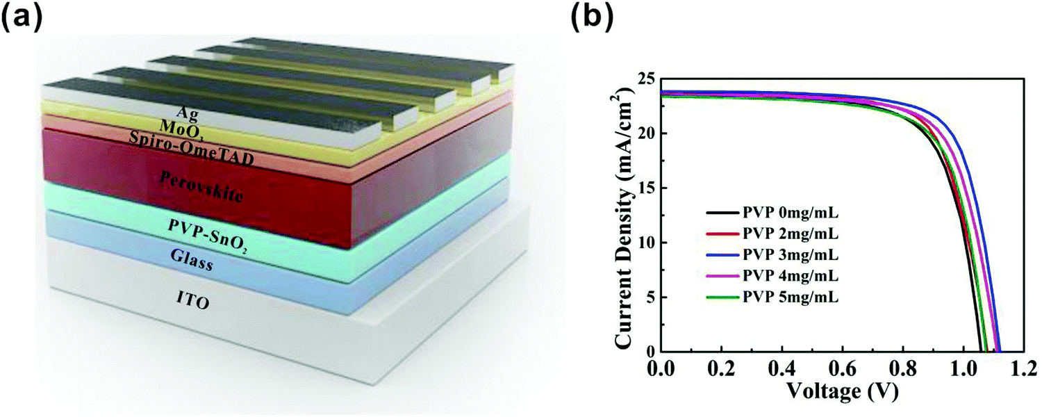 | ||
| Fig. 1 (a) Schematic view of the device structure in this work. (b) J–V characteristics of PSCs with PVP-SnO2 ETLs with various amounts of PVP. | ||
We optimized the performance of the PVP-SnO2-based solar cells by varying the content of PVP in the PVP-SnO2 precursor. As the PVP content increased from 2 mg mL−1 to 3 mg mL−1, the PCE of the corresponding PSCs was improved from 18.22% to 19.55%. When the concentration of PVP increased to 5 mg mL−1, the PCE was decreased to 17.80%. The conductivity of PVP is poor, so the higher concentration of PVP in SnO2 can damage the charge carrier mobility of the SnO2 layer. Accordingly, excessive PVP polymer cannot improve the performance of perovskite solar cells. The J–V curves for the PVP-SnO2-based devices with different PVP contents are provided in Fig. 1b, and the device performance parameters are summarized in Table 1.
| ETLs | V OC (V) | J SC (mA cm−2) | FF (%) | PCE (%) |
|---|---|---|---|---|
| PVP-SnO2 (2 mg mL−1) | 1.084 | 23.66 | 71.03 | 18.22 |
| PVP-SnO2 (3 mg mL−1) | 1.120 | 23.83 | 73.27 | 19.55 |
| PVP-SnO2 (4 mg mL−1) | 1.111 | 23.52 | 71.44 | 18.67 |
| PVP-SnO2 (5 mg mL−1) | 1.074 | 23.40 | 70.76 | 17.80 |
Fig. 2a shows the optical transmission spectra of the bare indium tin oxide (ITO), ITO/SnO2 and ITO/PVP-SnO2 (3 mg mL−1 PVP in SnO2 solution) films. It is found that the transmittances of the ITO/SnO2 and ITO/PVP-SnO2 films in the wavelength range of 300–500 nm are higher than the ITO without a coating. The ITO/PVP-SnO2 film has the best transmittance, thereby permitting more light to be absorbed by the perovskite layer. Therefore it proves that ITO/PVP-SnO2 has good optical quality. The introduction of SnO2 may change the reflectance over the entire wavelength region. Hence, the transmittances of the ITO/SnO2 and ITO/PVP-SnO2 films in the wavelength range of 300–500 nm are higher than the ITO without a coating, while the transmittances of the ITO/SnO2 and ITO/PVP-SnO2 films in the wavelength range of 500–900 nm are lower than the ITO without a coating.36 It is known that the electron mobility is a key parameter of ETLs in PSCs, so it is necessary to know the electron mobility of ETLs. The electron mobilities of different ETLs were measured using the space charge-limited current (SCLC) method,39 as shown in Fig. 2b. It is found that the electron mobility of PVP-SnO2 is 2.75 × 10⁻³ cm2 V−1 s−1, higher than that of SnO2 (2.24 × 10⁻³ cm2 V−1 s−1). The high electron mobility of the PVP-SnO2 based PSCs effectively promotes electron transfer and reduces charge accumulation at the ETL/perovskite interface, which improves the efficiency and suppresses hysteresis.27,36
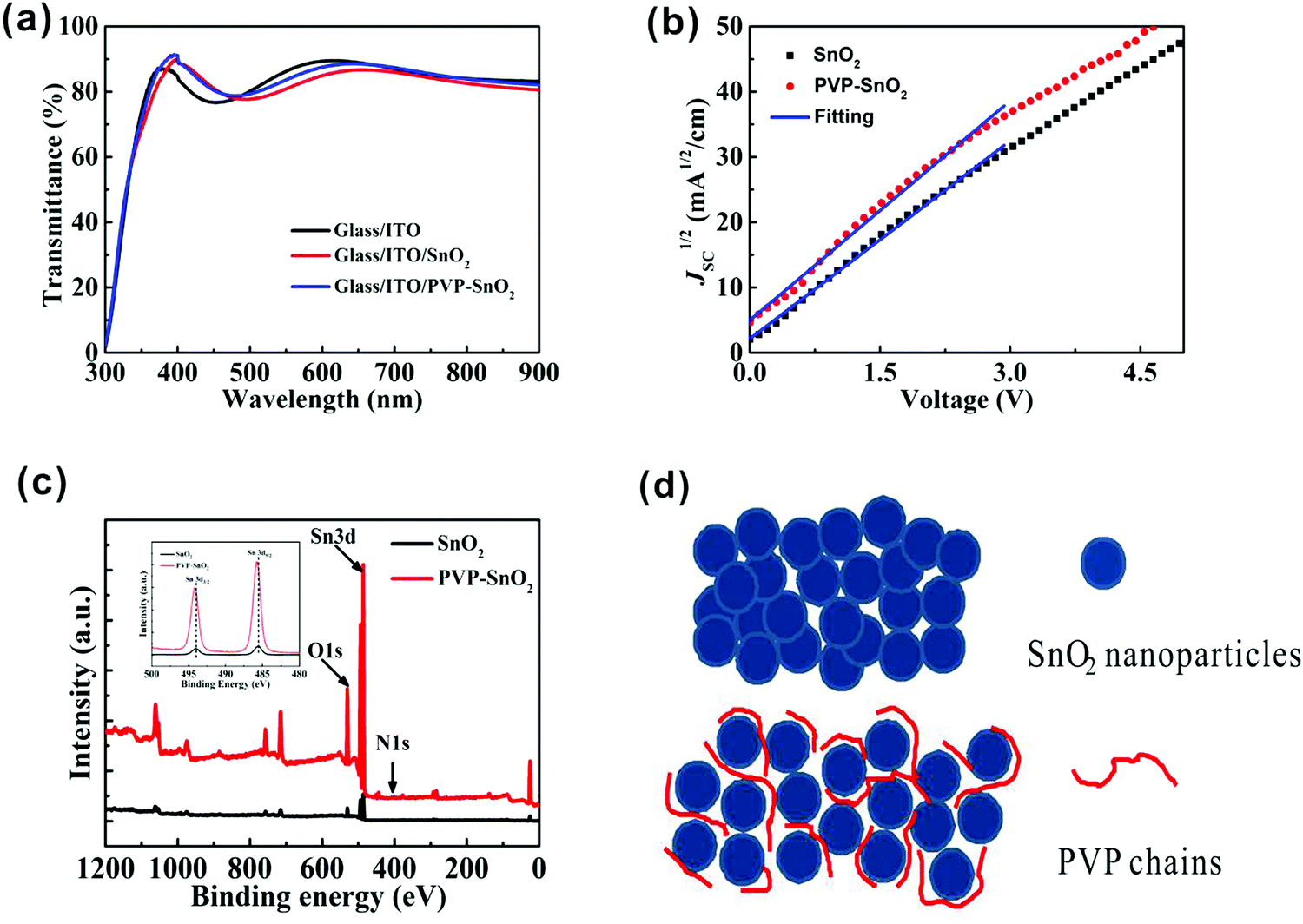 | ||
| Fig. 2 (a) Transmission spectra of ITO, ITO with SnO2, and ITO with PVP-SnO2 substrates. (b) J1/2–V plots for obtaining the electron mobilities of the SnO2 and PVP-SnO2 films using the SCLC model. (c) XPS spectra for the SnO2 and PVP-SnO2 films deposited on ITO substrates. The inset gives the XPS spectra of Sn 3d5/2 and Sn 3d3/2 of the SnO2 and PVP-SnO2 films. (d) Schematic images of the SnO2 and PVP-SnO2 films. | ||
The X-ray photoelectron spectra (XPS) of the SnO2 and PVP-SnO2 films deposited on ITO glass substrates were measured to confirm the existence of PVP, and the corresponding results are shown in Fig. 2c. All XPS measurements of binding energy data have been calibrated through the carbon 1s line at 284.8 eV. It is clear from these measurements that SnO2 shows distinct peaks of Sn and O. After the PVP treatment, the PVP-SnO2 film shows not only peaks of Sn and O, but also an additional peak located at 400 eV ascribed to N, which indicates the successful incorporation of PVP into SnO2. Meanwhile, the inset gives specific XPS spectra at Sn 3d peaks of the SnO2 and the PVP-SnO2 films. It is obvious that the Sn 3d peak of the PVP-SnO2 film was shifted to higher binding energy by 0.2 eV in contrast to that of the pristine SnO2, indicating that PVP is bound to SnO2.36 PVP can inhibit the agglomeration of SnO2 nanoparticles and improve the morphology of the SnO2 film,38 as shown in Fig. 2d. PVP can suppress the defects between the ETL layer and the perovskite and decrease the leakage current of the interface, thus improving the performance of perovskite solar cells. If the concentration of PVP is too large, the transportation of charge carriers will be damaged because of the poor conductivity of PVP. Therefore, a 2 mg mL−1 concentration of PVP is optimal for achieving the highest PCE and larger concentrations of PVP will inhibit the properties of perovskite solar cells.
The interface between the perovskite layer and the ETL layer has a significant effect on the device performance. Therefore, it is critical to examine the morphology of ETLs. We use atomic force microscopy (AFM) images to study the roughnesses of the pristine SnO2 and PVP-SnO2 films (3 mg mL−1 in SnO2 solution) deposited on ITO glass substrates as shown in Fig. 3a and b. It is also found that the roughness of the PVP-SnO2 film is higher (RMS: 3.72 nm) than that of the pristine SnO2 film without PVP (RMS: 2.44 nm). The surface roughness of the ETL compact layer could affect electron transport as it affects the contact area between the perovskite active layers and the ETL layer.40 An appropriately high roughness of PVP-SnO2 could lead to an increase in the contact area between the active layer and the ETL layer, thereby leading to improved charge transport.41,42
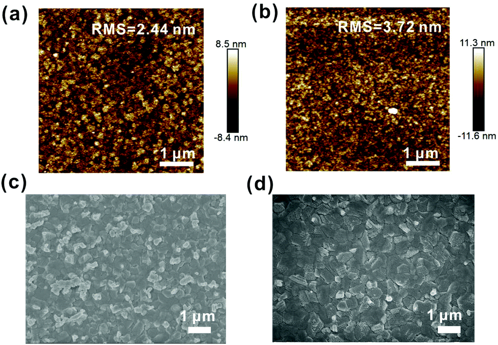 | ||
| Fig. 3 AFM images of the SnO2 (a) and the PVP-SnO2 (b) films deposited on ITO. SEM images of the perovskites coated on the SnO2 film (c) and the PVP-SnO2 film (d). | ||
The study of the perovskite film quality, including the grain size, crystallinity, surface coverage, etc., is very important for high-performance perovskite solar cells. Top-view SEM was used to study the surface morphology of perovskite films deposited on different ETLs, which is provided in Fig. 3c and d. It is apparent from these images that continuous pinhole-free films were obtained, which indicates films with full surface coverage. The crystal grain sizes of the perovskite film on PVP-SnO2 are more uniform and larger than those of the perovskite film deposited on SnO2. Moreover, the perovskite films deposited on both SnO2 and PVP-SnO2 have a white phase, which was confirmed to be PbI2.43 PVP can help the growth of the SnO2 layer, thus improving the morphology of the perovskite layer. As the SEM shows, the crystal grain size of the perovskite based on PVP-SnO2 is larger than that on SnO2, which can reduce the carrier recombination between the grain boundaries of the perovskite. As a result, the reverse saturation current is decreased and the open circuit voltage is increased. As we know, the growth of a perovskite is highly dependent on the substrate, and especially depends on the wetting properties of the substrate.44 The different growth behavior of SnO2 and PVP-SnO2 could be explained by two possible reasons: the different hydrophilic properties between SnO2 and PVP-SnO2 could be one reason; when the perovskite precursor was spin coated on the SnO2 layer, it wetted very well with SnO2 and nucleated everywhere due to the highly hydrophilic properties of SnO2, while the perovskite could only nucleate on some places of the PVP-SnO2 surface due to inferior hydrophilic properties compared with SnO2. On the other hand, the PVP-SnO2 film is dense and consists of particles; the PVP-SnO2 particles could provide effective nucleation sites to initiate perovskite crystal growth. Both of these could lead to larger perovskite crystals on PVP-SnO2 than on the SnO2 layer. As a result, the larger perovskite crystal grains are beneficial for electron transfer and then improve the photoelectric performance. The perovskite film on PVP-SnO2 has less PbI2 phase than the perovskite film on SnO2. According to the literature,45,46 an appropriate PbI2 amount is beneficial to the performance of PSCs.
XRD analysis of perovskite films deposited on different ETLs is also performed. The XRD patterns of the perovskite films spin-coated on the ITO/SnO2 and ITO/PVP-SnO2 substrates are shown in Fig. 4a. It is found that the perovskite film on PVP-SnO2 has almost the same diffraction peaks as the perovskite on the pure SnO2. A typical perovskite peak was found in perovskite films deposited on both ITO/SnO2 and ITO/PVP-SnO2 at 14.2°. At the same time, a peak at 12.7° corresponding to PbI2 was observed, which has a negative impact on the performance of perovskite solar cells. The perovskite on PVP-SnO2 has less PbI2 than the perovskite on SnO2, which is consistent with the conclusion of SEM in Fig. 3c and d.
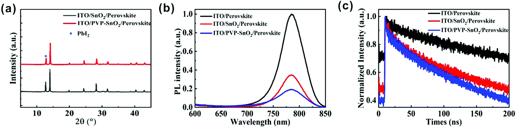 | ||
| Fig. 4 (a) X-ray diffraction (XRD) patterns of the perovskites deposited on different ETLs. (b) Photoluminescence (PL) spectra of the perovskite films deposited on ITO, SnO2 and PVP-SnO2 substrates. (c) Normalized time-resolved photoluminescence (TRPL) spectra of the perovskite films deposited on ITO, SnO2 and PVP-SnO2 substrates. | ||
Photoluminescence (PL) spectra and time-resolved photoluminescence (TRPL) spectra can be used to effectively analyze the interface charge transfer of PSCs. As shown in Fig. 4b, the PL spectra of the perovskites on ITO, SnO2 and PVP-SnO2 were measured to evaluate the interface charge transfer between the perovskite and the ETL. It can be clearly found that the PL peaks of the perovskite film spin-coated on ITO, ITO/SnO2 and ITO/PVP-SnO2 at 780 nm were quenched effectively when the SnO2 or PVP-SnO2 ETL was used, which demonstrated that the SnO2 ETL can help the electron extraction from the perovskite to the electrode. The perovskite on PVP-SnO2 exhibits more quenched PL than on SnO2, which is related to the more efficient electron transfer from the perovskite to the ETL. The results of TRPL show that the lifetime of the perovskite layer was significantly reduced when it was deposited on PVP-SnO2 compared to the one on SnO2, which indicates that efficient electron transfer occurred from the perovskite to PVP-SnO2 as shown in Fig. 4c. From all of the above analyses, we conclude that PVP-SnO2 as the ETL might improve the performance of perovskite solar cells.
We have proven that the performance of the device is improved by adding a small amount of PVP to the SnO2 solution. To confirm the positive effect of the PVP doping on the photovoltaic performance of PSCs, the performance of the devices based on SnO2 and PVP-SnO2 (3 mg mL−1 PVP) with the same device structure was compared, and the corresponding results are shown in Fig. 5a. For the PVP-SnO2 device, the best device shows an efficiency of 19.55% with VOC = 1.120 V, JSC = 23.83 mA cm−2 and FF = 73.27%. The highest efficiency of the device without the PVP additive is only 17.50%.
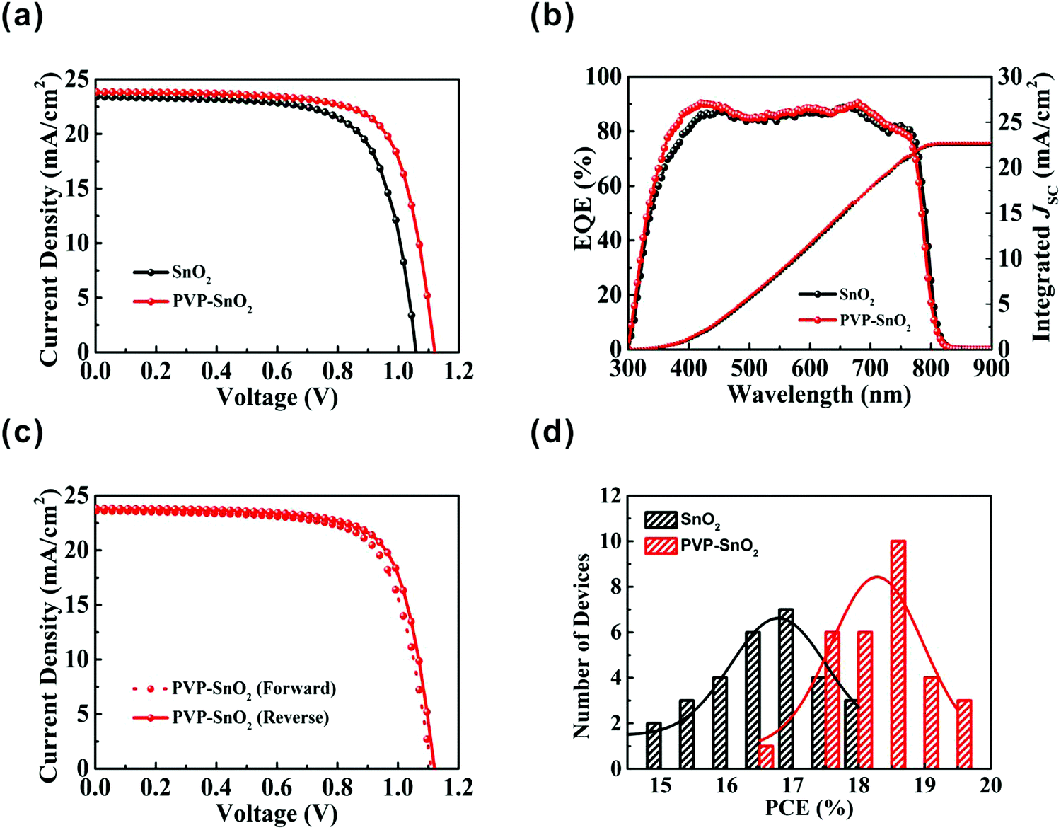 | ||
| Fig. 5 (a) J–V curves of the best-performing perovskite solar cells using the SnO2 and PVP-SnO2 ETLs measured under reverse scans. (b) The external quantum efficiency (EQE) spectra and the corresponding integrated JSC curves for the best-performance PSCs with different ETLs. (c) J–V curves of devices using the PVP-SnO2 ETL under reverse and forward scans. (d) The PCE distribution histogram of the planar type PSCs with different ETLs. | ||
Fig. 5b shows the external quantum efficiency (EQE) spectra and the corresponding integrated currents of the PSCs with different ETLs. The devices exhibit a broad peak above 80% in the range of 400 to 760 nm. The integrated current values calculated from the EQE spectra are 22.55 and 22.67 mA cm−2 for the devices with SnO2 and PVP-SnO2 as the ETL, respectively, which are close to the J–V measurements (within the error range). For the hysteresis test,47Fig. 5c shows the J–V curves of devices using the PVP-SnO2 ETL under reverse and forward scans. The PVP-SnO2-based device yielded a PCE of 19.55% from a reverse current–voltage scan, with VOC = 1.120 V, JSC = 23.83 mA cm−2 and FF = 73.27%. A small amount of hysteresis was observed with a forward scan yielding PCE = 18.76%. The detailed parameters of the reverse scan and forward scan of the two devices with the pure SnO2 and the optimized PVP-SnO2 are summarized in Table 2. The results show that the PVP-SnO2-based device has reduced hysteresis in comparison with the control device with SnO2.
| ETLs | Scanning direction | V OC (V) | J SC (mA cm−2) | FF (%) | PCE (%) | Average PCE (%) |
|---|---|---|---|---|---|---|
| SnO2 | Forward scan | 1.045 | 23.41 | 68.19 | 16.68 | 16.21 ± 3.03 |
| Reverse scan | 1.057 | 23.39 | 70.75 | 17.50 | ||
| PVP-SnO2 (3 mg mL−1) | Forward scan | 1.109 | 23.61 | 71.59 | 18.76 | 17.74 ± 3.01 |
| Reverse scan | 1.120 | 23.83 | 73.27 | 19.55 |
Fig. 5d shows the PCE distribution histogram for devices with different ETLs. It is apparent that the devices with the PVP-SnO2 ETL show better repeatability and smaller standard deviations than those with the SnO2 ETL. This result indicates that PVP-SnO2 can be used as a good candidate for the ETL in planar PSCs. Without any encapsulation, the long-term stability of the PSCs with SnO2 and PVP-SnO2 was investigated in a nitrogen environment. The shelf-stability of PSCs with different ETLs as a function of storage time is shown in Fig. 6. The device with the PVP-SnO2 ETL retains 88% of its initial PCE after 41 days of storage, while the device with the SnO2 ETL dropped to 80% of its initial PCE after 41 days. It indicates that the device with the PVP-SnO2 ETL is more stable than that with the SnO2 ETL, which is ascribed to the improved contact between the perovskite and the PVP-SnO2 ETL. It is known that the instability of perovskite solar cells is related to the degradation of the perovskite layer and the charge carrier transport layer. Because of the improved contact between the PVP-SnO2 ETL and the perovskite layer, the PVP-SnO2 based devices are more stable than the SnO2 based devices.
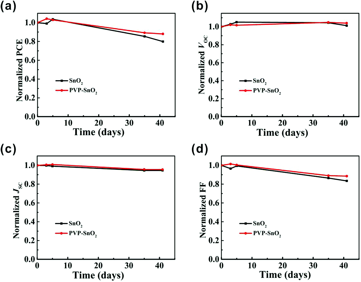 | ||
| Fig. 6 The shelf-stability of perovskite solar cells in a glove box without any encapsulation. Normalized (a) PCE, (b) VOC, (c) JSC and (d) FF. | ||
Conclusion
In summary, the incorporation of PVP into SnO2 improves the performance of planar perovskite solar cells. The characterization and analysis show that the PVP-SnO2 ETL promotes electron collection and transfer, which inhibits charge accumulation at the interface between the ETL and the perovskite, resulting in a high efficiency. In addition the crystal grain sizes of the perovskite film on PVP-SnO2 are more uniform and larger than the perovskite film deposited on SnO2. As an result, the PCE of the planar PSCs has increased to 19.55% from with the baseline of 17.50% from the control PSC with the SnO2 ETL, and the J–V hysteresis is alleviated. Therefore, we conclude that SnO2 with a suitable PVP content is a promising electron transport material for high-performance PSCs, and provides a viable method for improving the performance of perovskite solar cells.Experimental section
Materials
FAI, MABr, MACl, and spiro-OMeTAD were purchased from Xi’an Polymer Light Technology Corp. PbI2 was purchased from Sigma-Aldrich Company. The SnO2 colloid precursor was obtained from Alfa Aesar (tin(IV) oxide, 15% in H2O colloidal dispersion). Polyvinylpyrrolidone (PVP) was purchased from Shanghai Aladdin.Solar cell fabrication
ITO patterned glass substrates (1.5 cm × 1.5 cm) were ultrasonically cleaned by using detergent solution, deionized water, propanol and isopropanol for 15 minutes in each step. The ITO glass substrates were further cleaned by an ultraviolet ozone treatment for 20 minutes before depositing the ETL. In the process of preparing the device, two ETL solutions are mainly used, namely the SnO2 precursor solution and the PVP-SnO2 precursor solution. The SnO2 precursor solution was obtained by mixing 1 mL of the aqueous SnO2 solution with 3 mL of H2O. For the PVP-SnO2 precursor solution, first 1 mL of aqueous SnO2 solution was mixed with 3 mL of water, and then PVP (2–5 mg mL−1) was added to the SnO2 solution. The SnO2 and PVP-SnO2 precursors were stirred at room temperature for five hours. The different ETLs were deposited onto the treated ITO glass substrate by spin-coating at 4000 rpm for 40 s, and the samples were immediately annealed on a hotplate at 180 °C for 20 min. The preparation of the different ETLs is carried out in air. After cooling, the substrates were subjected to UV ozone treatment for 15 min, and transferred into a glove box for the deposition of the perovskite layer. The lead iodide solution was prepared as follows: 599.3 mg of PbI2 was dissolved in a mixed solvent of 1 mL of dimethylformamide (DMF) and anhydrous dimethyl sulfoxide (DMSO) at a temperature of 70 °C for one hour, wherein the volume ratio of DMF to DMSO was 9![[thin space (1/6-em)]](https://www.rsc.org/images/entities/char_2009.gif) :1. The mixture solution was synthesized by dissolving FAI (60 mg), MABr (60 mg) and MACl (6 mg) in 1 mL isopropanol and stirred for one hour. The perovskite films were deposited using a two-step spin coating method. First, the PbI2 solution was deposited onto different ETLs by spin-coating at 1500 rpm for 30 s, and then the substrates were annealed at 70 °C for 7 s to form PbI2 films. After spin-coating with the mixed solution, the substrates were annealed at 135 °C for 15 min to form a dark perovskite layer in air. After deposition of the perovskite layer, the substrates were transferred from the air to the glove box for the deposition of the HTL. The spiro-OMeTAD precursor solution was prepared by dissolving 72.3 mg spiro-OMeTAD, 35 μL of bis (trifluoromethane) sulfonimide lithium salt in acetonitrile (260 mg mL−1) and 30 μL of tert-butylpyridine in 1 mL chlorobenzene. The spiro-OMeTAD precursor solution was subsequently coated on the top of the perovskite film at 2500 rpm for 30 s. Note that after spin-coating the spiro-OMeTAD layer, the substrates were placed in air in a humidity-control box for 12 hours to ensure sufficient oxidation of the spiro-OMeTAD film. Finally, 7.5 nm of MoO3 and 100 nm of Ag were deposited by thermal evaporation at a vacuum condition of 9 × 10⁻⁵ Torr. The effective area of the perovskite cells reported in this work is 1.8 mm × 4.8 mm (0.0864 cm2).
:1. The mixture solution was synthesized by dissolving FAI (60 mg), MABr (60 mg) and MACl (6 mg) in 1 mL isopropanol and stirred for one hour. The perovskite films were deposited using a two-step spin coating method. First, the PbI2 solution was deposited onto different ETLs by spin-coating at 1500 rpm for 30 s, and then the substrates were annealed at 70 °C for 7 s to form PbI2 films. After spin-coating with the mixed solution, the substrates were annealed at 135 °C for 15 min to form a dark perovskite layer in air. After deposition of the perovskite layer, the substrates were transferred from the air to the glove box for the deposition of the HTL. The spiro-OMeTAD precursor solution was prepared by dissolving 72.3 mg spiro-OMeTAD, 35 μL of bis (trifluoromethane) sulfonimide lithium salt in acetonitrile (260 mg mL−1) and 30 μL of tert-butylpyridine in 1 mL chlorobenzene. The spiro-OMeTAD precursor solution was subsequently coated on the top of the perovskite film at 2500 rpm for 30 s. Note that after spin-coating the spiro-OMeTAD layer, the substrates were placed in air in a humidity-control box for 12 hours to ensure sufficient oxidation of the spiro-OMeTAD film. Finally, 7.5 nm of MoO3 and 100 nm of Ag were deposited by thermal evaporation at a vacuum condition of 9 × 10⁻⁵ Torr. The effective area of the perovskite cells reported in this work is 1.8 mm × 4.8 mm (0.0864 cm2).
Device characterization
The power conversion efficiencies of the perovskite solar cells were measured from current density–voltage (J–V) curves using a Keithley 2400 source under a simulated AM 1.5G spectrum with an intensity of 100 mW cm−2 (450 W Newport 94023A solar simulator). The devices were tested in an N2 glove box with the reverse scan (1.2 → 0 V, step 0.02 V, delay time 30 ms) and the forward scan (0 → 1.2 V, step 0.02 V, delay time 30 ms). The scanning electron microscopy (SEM) images of the perovskite surfaces and the cross-sections of the devices were measured using an S-4800 SEM setup. The external quantum efficiency (EQE) was measured using an Oriel LPCE-66894 in air. The transmission spectra of the films were measured by using a UV/vis spectrophotometer (PerkinElmer, Lambda 365). X-ray diffraction analysis was performed with a Bruker D8 Advance diffractometer operated at 30 kV and 10 mA at 2θ in the range of 10–60°, step 0.02° and scan speed 2.3° min−1.Conflicts of interest
There are no conflicts to declare.Acknowledgements
This work was supported by The National Key R&D Program of China (2018YFB1500102), Zhejiang Provincial Natural Science Foundation of China (LQ18F040002) and Zhejiang Provincial Key Laboratory (No. 2013E10022).References
- M. M. Lee, J. Teuscher, T. Miyasaka, T. N. Murakami and H. J. Snaith, Science, 2012, 338, 643 CrossRef CAS PubMed.
- P. Luo, Z. Liu, W. Xia, C. Yuan, J. Cheng and Y. Lu, ACS Appl. Mater. Interfaces, 2015, 7, 2708 CrossRef CAS PubMed.
- F. Zhang, X. Yang, H. Wang, M. Cheng, J. Zhao and L. Sun, ACS Appl. Mater. Interfaces, 2014, 6, 16140 CrossRef CAS PubMed.
- J. Burschka, N. Pellet, S. J. Moon, R. Humphry-Baker, P. Gao, M. K. Nazeeruddin and M. Grätzel, Nature, 2013, 499, 316 CrossRef CAS PubMed.
- H. Zhang, J. Cheng, D. Li, F. Lin, J. Mao, C. Liang, A. K. Y. Jen, M. Grätzel and W. C. Choy, Adv. Mater., 2017, 29, 1604695 CrossRef PubMed.
- E. H. Jung, N. J. Jeon, E. Y. Park, C. S. Moon, T. J. Shin, T. Y. Yang, J. H. Noh and J. Seo, Nature, 2019, 567, 511 CrossRef CAS PubMed.
- F. Fu, S. Pisoni, T. P. Weiss, T. Feurer, A. Wäckerlin, P. Fuchs, S. Nishiwaki, L. Zortea, A. N. Tiwari and S. Buecheler, Adv. Sci., 2018, 5, 1700675 CrossRef PubMed.
- A. Kojima, K. Teshima, Y. Shirai and T. Miyasaka, J. Am. Chem. Soc., 2009, 131, 6050 CrossRef CAS PubMed.
- M. He, B. Li, X. Cui, B. Jiang, Y. He, Y. Chen, D. O’Neil, P. Szymanski, M. A. EI-Sayed, J. Huang and Z. Lin, Nat. Commun., 2017, 8, 16045 CrossRef CAS PubMed.
- J. Qi, H. Xiong, C. Hou, Q. Zhang, Y. Li and H. Wang, Nanoscale, 2020, 12, 3646–3656 RSC.
- J. Qi, L. Li, H. Xiong, A. C. Wang, C. Hou, Q. Zhang, Y. Li and H. Wang, J. Mater. Chem. A, 2019, 7, 26154–26161 RSC.
- J. Qi, H. Xiong, G. Wang, H. Xie, W. Jia, Q. Zhang, Y. Li and H. Wang, J. Power Sources, 2018, 376, 46–54 CrossRef CAS.
- B. Wang, J. Iocozzia, M. Zhang, M. Ye, S. Yan, H. Jin, S. Wang, Z. Zou and Z. Lin, Chem. Soc. Rev., 2019, 48, 4854–4891 RSC.
- H. Tsai, W. Nie, P. Cheruku, N. H. Mack, P. Xu, G. Gupta, A. D. Mohite and H. L. Wang, Chem. Mater., 2015, 27, 5570 CrossRef CAS.
- R. Singh, A. Giri, M. Pal, K. Thiyagarajan, J. Kwak, J. J. Lee, U. Jeong and K. Cho, J. Mater. Chem. A, 2019, 7, 7151 RSC.
- B. Wang, M. Zhang, X. Cui, Z. Wang, M. Rager, Y. Yang, Z. Zou, Z. L. Wang and Z. Lin, Angew. Chem., Int. Ed., 2020, 59, 1611–1618 CrossRef CAS PubMed.
- W. Hu, W. Zhou, X. Lei, P. Zhou, M. Zhang, T. Chen, H. Zeng, J. Zhu, S. Dai, S. Yang and S. Yang, Adv. Mater., 2019, 31, 1806095 CrossRef PubMed.
- B. Wang, J. Iocozzia, M. Zhang, M. Ye, S. Yan, H. Jin, S. Wang, Z. Zou and Z. Lin, Chem. Soc. Rev., 2019, 48, 4854–4891 RSC.
- K. Domanski, E. A. Alharbi, A. Hagfeldt, M. Grätzel and W. Tress, Nat. Energy, 2018, 3, 61 CrossRef CAS.
- H. J. Snaith, A. Abate, J. M. Ball, G. E. Eperon, T. Leijtens, N. K. Noel, S. D. Stranks, J. T. Wang, K. Wojciechowski and W. Zhang, J. Phys. Chem. Lett., 2014, 5, 1511 CrossRef CAS PubMed.
- J. Wei, H. Li, Y. Zhao, W. Zhou, R. Fu, Y. L. Wang, D. Yu and Q. Zhao, Nano Energy, 2016, 26, 139 CrossRef CAS.
- J. Cao, B. Wu, R. Chen, Y. Wu, Y. Hui, B. W. Mao and N. Zheng, Adv. Mater., 2018, 30, 1705596 CrossRef PubMed.
- Y. C. Wang, X. Li, L. Zhu, X. Liu, W. Zhang and J. Fang, Adv. Energy Mater., 2017, 7, 1701144 CrossRef.
- P. Zhang, J. Wu, T. Zhang, Y. Wang, D. Liu, H. Chen, L. Ji, C. Liu, W. Ahmad, Z. D. Chen and S. Li, Adv. Mater., 2018, 30, 1703737 CrossRef PubMed.
- W. Ke, G. Fang, Q. Liu, L. Xiong, P. Qin, H. Tao, J. Wang, H. Lei, B. Li, J. Wan, G. Yang and Y. Yang, J. Am. Chem. Soc., 2015, 137, 6730 CrossRef CAS PubMed.
- T. Bu, J. Li, F. Zheng, W. Chen, X. Wen, Z. Ku, Y. Peng, J. Zhong, Y. B. Cheng and F. Huang, Nat. Commun., 2018, 9, 4609 CrossRef PubMed.
- Q. Jiang, L. Zhang, H. Wang, X. Yang, J. Meng, H. Liu, Z. Yin, J. Wu, X. Zhang and J. You, Nat. Energy, 2016, 2, 1 Search PubMed.
- W. Ke, G. Fang, Q. Liu, L. Xiong, P. Qin, H. Tao, J. Wang, H. Lei, B. Li, J. Wan, G. Yang and Y. Yan, J. Am. Chem. Soc., 2015, 137, 6730 CrossRef CAS PubMed.
- Y. Huang, S. Li, C. Wu, S. Wang, C. Wang and R. Ma, Chem. Phys. Lett., 2020, 137220 CrossRef CAS.
- W. Zhang, Y. Li, X. Liu, D. Tang, X. Li and X. Yuan, Chem. Eng. J., 2020, 379, 122298 CrossRef CAS.
- Z. Zhu, Y. Bai, X. Liu, C. C. Chueh, S. Yang and A. K. Y. Jen, Adv. Mater., 2016, 28, 6478 CrossRef CAS PubMed.
- W. Q. Wu, D. Chen, Y. B. Cheng and R. A. Caruso, Sol. RRL, 2017, 1, 1700117 CrossRef.
- S. Jeong, S. Seo, H. Park and H. Shin, Chem. Commun., 2019, 55, 2433 RSC.
- J. Zhang, T. Zhang, L. Jiang, U. Bach and Y. B. Cheng, ACS Energy Lett., 2018, 3, 1677 CrossRef CAS.
- F. Qi, X. Deng, X. Wu, L. Huo, Y. Xiao, X. Lu, Z. Zhu and A. K. Y. Jen, Adv. Energy Mater., 2019, 9, 1902600 CrossRef CAS.
- D. Yang, R. Yang, K. Wang, C. Wu, X. Zhu, J. Feng, X. Ren, G. Fang, S. Priya and S. F. Liu, Nat. Commun., 2018, 9, 3239 CrossRef PubMed.
- J. Wei, F. Guo, X. Wang, K. Xu, M. Lei, Y. Liang, Y. Zhao and D. Xu, Adv. Mater., 2018, 30, 1805153 CrossRef PubMed.
- C. E. Small, S. Chen, J. Subbiah, C. M. Amb, S. W. Tsang, T. H. Lai, J. R. Reynolds and F. So, Nat. Photonics, 2012, 6, 115–120 CrossRef CAS.
- L. La Notte, P. Cataldi, L. Ceseracciu, I. S. Bayer, A. Athanassiou, S. Marras, E. Villari, F. Brunetti and A. Reale, Mater. Today Energy, 2018, 7, 105 CrossRef.
- Z. Ma, Z. Tang, E. Wang, M. R. Andersson, O. Inganäs and F. Zhang, J. Phys. Chem. C, 2012, 116, 24462 CrossRef CAS.
- Q. Liu, X. Zhang, C. Li, H. Lu, Z. Weng, Y. Pan, W. Chen, X. C. Hang, Z. Sun and Y. Zhan, Appl. Phys. Lett., 2019, 115, 143903 CrossRef.
- R. Ranjan, A. Prakash, A. Singh, A. Singh, A. Garg and R. K. Gupta, J. Mater. Chem. A, 2018, 6, 1037 RSC.
- Q. Jiang, Z. Chu, P. Wang, X. Yang, H. Liu, Y. Wang, Z. Yin, J. Wu, X. Zhang and J. You, Adv. Mater., 2017, 29, 1703852 CrossRef PubMed.
- C. Bi, Q. Wang, Y. Shao, Y. Yuan, Z. Xiao and J. Huang, Nat. Commun., 2015, 6, 7747 CrossRef CAS PubMed.
- Y. C. Kim, N. J. Jeon, J. H. Noh, W. S. Yang, J. Seo, J. S. Yun, A. Ho-Baillie, S. Huang, M. A. Green, J. Seidel, T. K. Ahn and S. I. Seok, Adv. Energy Mater., 2015, 6, 1502104 CrossRef.
- B. Shi, X. Yao, F. Hou, S. Guo, Y. Li, C. Wei, Y. Ding, Y. Li, Y. Zhao and X. Zhang, J. Phys. Chem. C, 2018, 122, 21269–21276 CrossRef CAS.
- P. Liu, W. Wang, S. Liu, H. Yang and Z. Shao, Adv. Energy Mater., 2019, 9, 1803017 CrossRef.
| This journal is © The Royal Society of Chemistry 2020 |