
 Open Access Article
 This Open Access Article is licensed under a Creative Commons Attribution-Non Commercial 3.0 Unported Licence
High doping efficiency in p-type Al-rich AlGaN by modifying the Mg doping planes
Xinjia
Qiu
 ,
Yingda
Chen
,
Enze
Han
,
Zesheng
Lv
,
Zhiyuan
Song
and
Hao
Jiang
*
,
Yingda
Chen
,
Enze
Han
,
Zesheng
Lv
,
Zhiyuan
Song
and
Hao
Jiang
*
State Key Laboratory of Optoelectronic Materials and Technologies, School of Electronics and Information Technology, Sun yat-sen University, Guangzhou 510275, People's Republic of China. E-mail: stsjiang@mail.sysu.edu.cn
First published on 30th March 2020
Abstract
High doping efficiency of the Mg dopant in Al-rich AlGaN is highly desired for AlGaN based deep ultraviolet optoelectronics. In this work, the Mg doping planes were modified by a pulsed group-III source, according to first-principles calculation results on Mg substituting Al or Ga on the surface and in the bulk of Ai-rich AlGaN. The Mg-delta-doped AlxGa1−xN (x ∼ 0.42) layer, using a pulsed Ga source to modify the doping planes, exhibits a very high hole concentration of 8.3 × 1018 cm−3, which is 67% higher than that of the reference one. A record doping efficiency of 51.9% was achieved and the consequent resistivity is as low as 0.51 Ω cm. It was found that the Mg incorporation was significantly enhanced and the acceptor activation energy (EA) was substantially reduced, contributing to the high doping efficiency. The improved incorporation is attributed to the enhanced Mg substitution for Al at the doping planes and the increased substitution for Ga in the bulk by the modification, whereas the decreased EA is ascribed to the enlarged valence-band bending. This method provides a simple and effective way to realize efficient p-type doping of Al-rich AlGaN.
1. Introduction
Ternary AlGaN alloys have been recognized as promising materials for realizing deep ultraviolet (DUV) optoelectronic devices with operating wavelengths down to 200 nm.1–3 For the development of high performance AlGaN-based DUV devices, high-conductivity p-type Al-rich AlxGa1−xN (x ≥ 0.4) is essential. Many studies have shown that enhancing the p-type conductivity has a significant effect on the improvement of both the electrical and optical properties of AlGaN DUV optoelectronics.4–8 However, achieving efficient p-type doping in Al-rich AlGaN is still a great challenge for the following reasons: (i) the limited solubility of magnesium (Mg), which is caused by the high formation enthalpies of Mg substitution for Ga or Al; (ii) the high activation energy for Mg-doped AlxGa1−xN increasing from ∼170 to 630 meV for x = 0 to x = 1, due to the low valence band maximum, the deep impurity levels, and the heavy effective mass of the holes; and (iii) the strong self-compensation arising from the presence of donor-like native defects and/or complexes.9 These factors have led to the fact that the doping efficiency of the p-type Al-rich AlGaN reported in most literature is usually less than or around 1%.5,10,11So far, a number of p-type doping approaches, including superlattice (SL) doping,12 Mg delta (δ) doping,13 polarization-induced hole doping,7 and Mg–Si alternative co-doping,14 have been developed to improve the p-type doping efficiency of Al-rich AlGaN. From the perspective of the mechanism, these techniques were mainly focused on reducing the acceptor ionization energy by energy-band modulation. There are few reports, however, on the efficient incorporation of the Mg dopant. It is known that the solubility of impurities can be enhanced near a semiconductor surface such as Si(001), because the energy of impurities is reduced due to the inherent stress relief near the surface.15 Such surface effects are therefore expected to be utilized to improve the incorporation efficiency of the Mg dopant in Al-rich AlGaN.
Delta doping is a long established approach to spatially confine dopants by interrupting the growth of the matrix material to make the dopants deposit on the exposed surface during epitaxial growth. In this method, the doping layer is divided into multiple periodic bulk layers and temporary surfaces, thus providing conditions for making full use of the surface and bulk effects of dopant impurity incorporation. In this work, first-principles calculations were utilized to analyze the behaviors of substituting Mg for Ga and Al on the surface and in the bulk of AlGaN. On the basis of the calculation results, it was proposed to improve the incorporation efficiency of the Mg dopant in Al-rich AlGaN by modifying the Mg-δ-doping planes (i.e., doping surface) with a pulsed group-III source. The p-type doping efficiency was significantly improved in the AlGaN epilayer by modifying the δ-doping planes with a pulsed Ga source. The effects of pulsed group-III sources on the Mg incorporation on the doping plane and in the bulk were investigated in detail. The mechanisms for the efficiency improvement were interpreted mainly in terms of dopant incorporation and activation energy. Furthermore, the applicability of this doping strategy was verified by the fabrication of all Al-rich AlGaN pn junctions.
2. Experimental section
Computational method
The first-principles calculations of total energies were performed within the framework of density functional theory (DFT), implemented in the Vienna ab initio simulation package (VASP).16,17 The interactions between valence electrons and ion cores were treated by Blöchl's all-electron-like projector augmented wave (PAW) method.18 The electronic exchange and correlation were described in the generalized gradient approximation (GGA), using the Perdew–Burke–Ernzerhof (PBE) functional.19 A cutoff energy of 425 eV was used for the plane-wave basis set, while the Ga (3d104s24p1), Mg (3s2), Al (3s23p1), and N (2s22p3) states are treated as valence electrons. Bulk calculations were conducted using a 3 × 3 × 3 supercell with 108 atoms and the Brillouin zone was sampled on a 3 × 3 × 3 k-point Monkhorst–Pack mesh.20 In the case of the surface, a (3 × 3) supercell consisting of a six-bilayer thick slab along with a vacuum layer of ∼12 Å was used to describe the AlGaN(0001) surface with a 3 × 3 × 1 k-point mesh. The three bottom AlxGa1−xN bilayers were fixed in the appropriate bulk-optimized configuration to simulate the surface growth, while all the atoms were fully relaxed in the bulk calculations. Convergence with respect to the plane-wave cutoff energy and k-point sampling has been carefully checked. The convergence criterion for the forces of structure relaxations is 0.01 eV Å−1.In the calculations, the formation energy (Ef) of Mg was the main object of our research as Ef is a key factor for the Mg incorporation efficiency. Generally, Ef of neutral Mg impurities can be calculated by21
 | (1) |
| μAl/Ga = μAlN/GaN − μN, | (2) |
| 3μMg + 2μN = μMg3N2. | (3) |
 | (4) |
Growth and characterization of p-AlGaN epitaxial films
The AlGaN epilayers were grown on 2 inch c-plane sapphire substrates by the low-pressure metalorganic chemical vapor deposition (MOCVD) method. Trimethyl-gallium (TMGa), trimethyl-aluminum (TMAl), trimethyl-indium (TMIn), and ammonia (NH3) were used as precursors for Ga, Al, In, and N, respectively, while bis-cyclopentadienyl magnesium (Cp2Mg) was employed for p-type doping. Hydrogen was used as a carrier gas through the whole growth run. The basic epi-structure consists of a 400 nm-thick AlN layer, an about 350 nm-thick Mg-δ-doped AlxGa1−xN (x ∼ 0.4) layer grown at 1080 °C, and an 8 nm-thick Mg-doped GaN cap layer with a doping level of ∼7 × 1019 cm−3 for an ohmic contact. A control sample was at first grown by the Mg-δ-doping method with In as a surfactant, in which the group-III sources and Cp2Mg were alternately opened and closed, while NH3 was open all the time.24 As a surfactant, the flow rate of TMIn was kept at the optimized value of 140 sccm during the growth period of 20 nm AlxGa1−xN (x ∼ 0.4). An optimized V/III ratio of 3140 was used for depositing AlGaN. In the process of δ doping, the NH3 flow was held constant, which is equivalent to an infinite V/III ratio condition (i.e., an extremely N-rich condition). The second sample was obtained by introducing a pulsed TMGa flow (PTGF) into the doping process, right after the 48 s Mg-δ-doping step in each doping period. The third sample was grown with the same recipe, except that the PTGF was replaced by a pulsed TMAl flow (PTAF). The duration time of the PTGF or PTAF was set at an optimized value of 4 s. Fig. 1 outlines the source flow sequence during one period of the modified δ-doping process and the schematic epitaxial structure of the Mg-δ-doped AlGaN sample grown with the PTGF. | ||
| Fig. 1 Flow sequence of the modified Mg-δ doping process with In as a surfactant (a) and the schematic side view of the epitaxial structure of the p-AlGaN grown with the PTGF (b). | ||
After the growth, all the three samples were thermally annealed at 730 °C for 25 min in an N2 atmosphere to dissociate the Mg–H complex. Temperature-dependent Hall-effect measurements were carried out to characterize the electrical properties of the p-type samples using the standard Van der Pauw geometry. Circular ohmic contacts with a diameter of 0.5 mm were formed by depositing a Ni/Au metal stack followed by annealing at 550 °C in an oxygen atmosphere for 2 min. During the measurements, the part of the p-GaN cap layer outside the ohmic contacts was removed to eliminate the effect of parallel conduction. Secondary ion mass spectroscopy (SIMS) measurements were performed to investigate the depth profiles of the Al and Ga secondary ionic intensity and Mg atomic concentration in the three samples. Transmittance spectra of the deposited p-AlGaN layers grown on double-side polished (0001) sapphire substrates were recorded using a Shimadzu UV2550 ultraviolet-visible spectrophotometer. The Al composition and structural crystalline quality were determined by high-resolution X-ray diffraction (HRXRD) measurements using a Bruker D8 Discover instrument.
Fabrication and characterization of the AlGaN PN diode
Full Al-rich AlGaN pn-junctions were fabricated and characterized to verify the feasibility of the p-type Al-rich AlGaN layer grown with the modified Mg-δ-doping plane. The epitaxial structure comprises a 500 nm-thick optimized high-temperature AlN buffer layer, a 360 nm-thick Si-doped Al0.4Ga0.6N layer (n ∼ 2.7 × 1018 cm−3), and a 170 nm-thick p-type AlxGa1−xN (x ∼ 0.4) layer deposited by the PTGF method. Device processing was started with circular mesa formation using conventional photolithography and dry-etching down to the n-Al0.4Ga0.6N layer. After the surface treatment, n-type ohmic contacts made of a Ti/Al/Ni/Au metal stack were deposited by electron-beam evaporation and alloyed by a rapid thermal annealing process at 830 °C in an N2 atmosphere for 30 s. The p-type ohmic contacts were made by depositing Ni/Au and annealed at 550 °C in an ambient atmosphere. Current–voltage (I–V) characteristics of the fabricated devices were measured using a Keithley 4200-SCS semiconductor characterization system under dark and UV-illuminated conditions. The illumination was supplied by a UV light emitting diode with a peak wavelength of 266 nm.3. Results and discussion
The incorporation behavior of the Mg dopant in the Mg-δ-doped AlxGa1−xN (x ∼ 0.4) epitaxial layer, in which the Al composition is typically ∼40% in the bulk and ∼80% at the δ-doping plane,24 was at first investigated using first-principles calculations. In the calculations, the value of the N chemical potential, μN, was set to be close to μ[N2] (i.e., the energy of N in a N2 molecule) to simulate the N-rich growth condition in our work. Compared with the N atoms, the group-III metal atoms are the next-nearest (NN) atoms to the Mg substitutes. Since the number of N atoms can be regarded as constant, only the effect of the number change of NN Ga atoms on the Ef of Mg acceptors is considered, while the effect of the NN Al-atom number can be treated as the opposite. Fig. 2(a) and (b) show the Ef of Mg substitutes for Ga (MgGa) and Al (MgAl) acceptors in the Al0.4Ga0.6N bulk and at the Al0.8Ga0.2N growth surface under N-rich conditions as a function of the NN Ga-atom number. It can be seen that the Ef values of MgAl and MgGa in the surface are negative, suggesting favorable Mg substitution in this case. The Ef of MgAl is lower than that of MgGa and increases as the NN Ga-atom number increases. In contrast to the surface case, Ef in the bulk is positive, which limits the Mg incorporation, as shown in Fig. 2(b). The Ef of MgAl is larger than that of MgGa in the bulk of the Al0.4Ga0.6N alloy, suggesting that the Mg atoms prefer to replace Ga sites rather than Al sites. It was also found that the Ef values of MgGa and MgAl decrease monotonically with increasing NN Ga-atom number (i.e. the Ga composition). These characteristics can be mainly ascribed to the larger cohesive energy of the Al–N bond (2.88 eV) as compared to that of the Ga–N bond (2.24 eV).25 Besides, it has been proposed that the Ef of a p-type dopant with a larger atomic size than the host atom increases with the increase of compressive stress.26 Therefore, the enhanced compressive strain, leading from MgAl due to the smaller covalent radius of Al (1.18 Å) than Ga (1.26 Å) and the larger covalent radius of Mg (1.30 Å), may also contribute to the larger Ef of MgAl. According to the above calculation results, the introduction of a pulsed Ga or Al source is expected to have a significant effect on the Mg incorporation at the δ-doping plane. Therefore, the samples grown with the PTFG and PTAF were prepared together with the control sample for comparison. | ||
| Fig. 2 Formation energies of MgAl and MgGa in the neutral charge state as a function of the NN Ga atom numbers on the growth surface (a) and in the bulk (b) under N-rich conditions. The supercell geometry of the Al0.4Ga0.6N disordered alloy (c) and Al0.8Ga0.2N disordered alloy (d) with one Mg substitution atom, surrounded by 3 next-nearest Ga atoms (as examples), which are labeled by black circles. | ||
Table 1 summarizes the Hall measurement results of the three p-type AlGaN samples determined at room temperature (RT). It can be found that the sample grown with the PTGF shows superior electrical properties over the control sample and the sample grown with the PTAF. A p-type conductivity with a high hole concentration (p) of 8.30 × 1018 cm−3, a low resistivity of 0.51 Ω cm, and a hole mobility of 1.47 cm2 V−1 s−1 was achieved in the sample grown with the PTGF. The hole concentration was significantly increased, contributing most to the enhanced electrical conductivity with a resistivity comparable to those of the state-of-the-art p-GaN.27,28 Besides, the hole mobility of the PTGF sample is also slightly higher than that of the control sample, despite the higher hole concentration. This is likely due to the reduced dislocation scattering. The HRXRD rocking-curve width for the (0002) peak, which mainly reflects the screw-component dislocation density, decreases from 429 to 261 arcsec by the introduction of the PTGF. Compared with the control sample, the sample grown with the PTAF, however, demonstrated a remarkably lower hole concentration of 4.60 × 1017 cm−3 and a consequently high resistivity of 5.38 Ω cm. These results indicate that the pulsed precursors at the δ-doping plane have an important effect on the hole concentration.
| Sample | Hole concentration (cm−3) | Mobility (cm2 V−1 s−1) | Resistivity (Ω cm) |
|---|---|---|---|
| Control | 4.97 × 10¹⁸ | 1.35 | 0.93 |
| w/PTGF | 8.30 × 10¹⁸ | 1.47 | 0.51 |
| w/PTAF | 4.61 × 10¹⁷ | 2.52 | 5.38 |
SIMS measurements were then performed to investigate the Mg incorporation in the different p-AlGaN samples. Fig. 3 depicts the SIMS depth profiles of Mg, Al and Ga along the growth direction. Clear periodic oscillations were observed in the profile of the Mg atomic concentration (CMg) in the three samples, which are consistent with the feature of δ-doping. The depth profiles of the Al and Ga intensity also show oscillations with the same period as CMg, which are ascribed to the preferential dissociation of Ga–N bonds during the purge step and the substitution of Mg at Al and Ga sites. As a result of the dissociation, the Ga intensity decreases to the valley point of the oscillation profile, which can be recognized as the positions of the δ-doping plane (e.g., the vertical red line in Fig. 3a). During the δ-doping process, the Mg atoms not only occupy group III vacancies generated by In and Ga desorption during the purge step, but also tend to replace Al atoms due to the lower Ef of MgAl on the AlxGa1−xN surface. Consequently, it is shown that the peak positions of the CMg profile (the vertical red dashed line) correspond to the valley positions of the Al-intensity profile, which slightly deviated from the δ-doping plane backward. The backward diffusion of the δ-doped Mg atoms is accompanied by Mg substitution on Ga and Al sites, leading CMg to reach a valley point between two δ-doping planes. In this process, the attenuation of CMg mainly depends on the substitution of Ga by Mg. This is because the Ef of MgGa is lower than that of MgAl in the bulk case, i.e. substituting Mg for Ga is more energetically favorable. Therefore, the valley point of the CMg profile corresponds to the peak position of the Ga-intensity profile, indicated as the vertical black dashed line shown in Fig. 3a.
 | ||
| Fig. 3 SIMS depth profiles of Al, Ga, and Mg obtained from the (a) control, (b) PTGF, and (c) PTAF samples. | ||
Moreover, it is notable that the depth profile of CMg shows an upward slope along the growth direction of the control sample. According to the results shown in Fig. 2, when the growing surface is covered by newly added layers during the epitaxy, the inner Mg atoms tend to segregate to the new surface to regain equilibrium because of the lower Ef of Mg substitutes on the surface, while a part of Mg substitutes remain in the layer that has been converted into the bulk. Consequently, CMg increases gradually along the growth direction. This is the case for the forward diffusion and incorporation of δ-doped Mg atoms, which is dominated by the competition between the substitution of Al by Mg on the growing surface and the substitution of Ga by Mg in the bulk.
For the PTGF sample, the entire incorporation of Mg is significantly enhanced, as illustrated in Fig. 3b. The average CMg, calculated by integrating the depth profile of CMg over the p-AlGaN layer and dividing the integral by the layer thicknesses, is 1.6 × 1019 cm−3, about 1.4 times higher than that of the control sample and indicating a very high doping efficiency ηp (= p/CMg) of 51.9%. It was found that the average peak and valley values of the CMg profile (Cp,av and Cv,av) are 2.1 × 10¹⁹ and 1.4 × 10¹⁹, respectively; both are higher than the corresponding values of the control sample. Meanwhile, the Al and Ga profiles show a decrease in the average valley and peak intensities (Iv,av and Ip,av), respectively, as compared to the control sample. This means that the Mg substitution for Al is enhanced by introducing the PTGF at the δ-doping planes and the substitution for Ga is also increased in the layer between the δ-doping planes.
It can be reasoned that the supplement of Ga atoms by the use of the PTGF prevents the δ-doped Mg from diffusing into the interface of the next growth layer due to the much higher Ef of MgGa compared to that of MgAl on the surface of the grown layer. The Mg incorporation on the underlayer surface is therefore enhanced, leading to a slightly higher value of Cp,av. On the other hand, the PTGF also makes a small amount of Ga incorporate into the next growth layer, which is evidenced by the enhanced Ga intensities at the valley points and the increased growth rate with respect to the control sample. The increase of Ga incorporation reduces the Ef of MgGa and MgAl in the bulk, especially the Ef of MgGa, and thus increases the Mg incorporation. As a result, the value of Cv,av is significantly increased and the Ip,av of the Ga intensity profile is correspondingly decreased. Such an Mg-incorporation enhancement in the bulk also suppresses the Mg segregation to the growing surface, leading to a CMg profile without inclination as shown in Fig. 3b.
On the contrary, as shown in Fig. 3c, the Mg incorporation is inhibited markedly by introducing the PTAF. Compared with the control sample, the Iv,av value of the Al profile increases, while the Ip,av value of the Ga profile decreases for the PTAF sample. The decrease of Ip,av should be due to the lowered Ga incorporation by introducing the PTAF, rather than Mg substituting Ga in the layer, because the corresponding Cv,av of the Mg profile is also decreased. It has been reported that the incorporation of Ga is generally blocked by the Al incorporation during the growth of AlGaN, because competitive adsorption of Al atoms hinders the incorporation of Ga atoms.29 The above argument is also supported by the observed reduction in the growth rate (i.e., thickness) of the PTAF sample (Fig. 3c).
According to the change of CMg and the corresponding changes of the Al and Ga intensity, the mechanism for the reduced Mg incorporation in this case can be interpreted in terms of the diversion effect of the PTAF on the δ-doped Mg and its blocking effect on the MgGa formation. Under the extremely Al-rich condition with the use of the PTAF, the δ-doped Mg diffused to the surface of the grown layer is diverted to the surface of the growing layer, resulting in a reduction of Cp,av at the δ-doping planes. Although the growing surface shares the doped Mg due to the lower Ef of MgAl, in the bulk layer transformed from the surface, the Mg incorporation decreases significantly due to the higher Ef of MgGa and MgAl caused by the increase of Al incorporation. The incorporation of Mg is thus reduced overall. In addition, the segregation of Mg was also improved due to the diversion effect of the PTAF at the δ-doping planes. However, as the Mg incorporation in the bulk layer has not been enhanced, the effect of segregation inhibition is not as significant as that of the PTGF.
Besides the Mg incorporation, the activation energy (EA) of the Mg acceptor is also a key factor in enhancing the doping efficiency. Temperature-dependent Hall-effect measurements were therefore performed on the PTGF and control samples from 300 K to 560 K in 15 K increments. Fig. 4 presents the Arrhenius plots of hole concentration versus reciprocal temperature for the two samples. The value of EA, the acceptor concentration (NA), and the compensating donor concentration (ND) can be extracted by fitting the data points in the Arrhenius plot to the formula
 | (5) |
 | ||
| Fig. 4 Temperature-dependent hole concentration for the PTGF and control samples. The fitting curves are shown as solid lines. | ||
The very low values of EA could be due to the strong band modulation (i.e., composition modulation) effect resulting from the delta-doping process, as shown in Fig. 3. It was found from the SIMS data that the Al compositions around the δ-doping plane are higher, leading to a self-formed periodic structure with a quantum well (QW) and a graded barrier (GB). In order to clarify the effect of band modulation on the lowered EA by introducing the PTGF, we simulated the valence band profiles along the growth direction for the control and PTGF samples by self-consistently solving the 1D coupled Schrödinger–Poisson equations with the TCAD tool Silvaco Atlas. In the simulations, the depth profiles of Al and Ga compositions were deduced from the SIMS results and verified by fitting the XRD 2θ–ω scan curves of the (0002) reflection. The thicknesses of the QW and GB regions were estimated to be ∼12.5 and 5.7 nm, and 13.9 and 6.8 nm for the control and PTGF samples, respectively, while the Al compositions of the QW and GB peak were ∼42.4% and 81%, and 41.7% and 80.8%, respectively. The increased thicknesses of the QW and GB regions of the p-AlGaN layer grown with the PTGF are ascribed to the increased incorporation of Ga atoms. Also, the enhanced incorporation contributes to the lower minimum of the Al composition (Fig. 5).
 | ||
| Fig. 5 HRXRD (0002)-plane 2θ–ω scan curves for the PTGF sample and control sample. | ||
The resulting valence band diagrams are shown in Fig. 6. As seen in Fig. 6a and b, the valence band bends upward at the QW/GB interface (dashed ring) due to the strong internal polarization fields in the III-nitrides.31 Consequently, the holes in the two p-AlGaN samples are contributed by the following parts: (1) the thermally ionized holes arising from the QW regions where the Mg acceptor level (EMg) is above the Fermi level (almost no holes from the acceptors in the GB regions due to the high ionization energy); (2) the holes released from the Mg acceptors in the QW and GB regions where EMg is below the Fermi level; and (3) the holes accumulated at the QW/GB interfaces where the valence band bends and exceeds the Fermi level, forming a two-dimensional hole gas (2DHG). The quantity of holes from parts (1) and (2) should be increased in the case of doping with the PTGF, because of the significantly increased CMg, which is mainly contributed by the increment of MgGa acceptors with lower Ef in part (1) and by the increment of MgAl acceptors in part (2). In part (3), more 2DHG is expected to accumulate at the heterointerface of the δ-doping layer grown with the PTGF, due to the extended interfacial band bending area as shown in Fig. 6c. Also shown in Fig. 6b and c is the valence band of the control sample, in which the Al compositions of the peak and valley remain unchanged, while the thicknesses of the QW and GB become the same as those of the PTGF sample. It can be seen that the band bending of the PTGF sample is still slightly deeper at the QW/GB interfaces, indicating that the band bending mainly results from the polarization field introduced by the change of the Al composition, rather than the thickness change of the QW and GB.
 | ||
| Fig. 6 The simulated valence band diagrams of the control (a) and the PTGF (b) samples. The vertical green dashed lines indicate the positions of δ-doping planes. A detailed diagram for comparing the valence band profiles around the QW/GB interface is shown in (c). The green lines in (b) and (c) are the valence band of the control sample with the thicknesses of the QW and GB consistent with those of the PTGF sample. | ||
Besides, it should be noted that the EA of the PTGF sample may also be lowered by the enhanced Coulomb interaction between the ionized acceptors and the increased screening of the Coulomb potential by the free carriers.32,33 The enlarged band bending combined with the increased acceptor concentration led to a much lower equivalent EA value in the PTGF sample.
The optical transmission spectra of the three samples were also recorded under the normal-incidence condition. As shown in Fig. 7a, the transmittance (T) of the transmission peaks is larger than 80% at wavelengths above the absorption edge of the three thermally-annealed p-AlGaN samples, even without considering the reflection loss. Such high transmittance is beneficial for DUV optoelectronic applications. Assuming the absorption coefficient α ∼ ln(1/T) corresponding to the direct energy band gap (Eg) of AlGaN, the equivalent Eg of our p-AlGaN layers with QW and QB structure can be estimated by extrapolating the linear portion of the (αhν)2versus photon energy (hν) plot. The obtained values of Eg are 4.43, 4.47, and 4.39 eV for the control, PTGF, and PTAF samples, respectively. These values are contrary to those expected from the Al compositions of the three samples, in which the PTAF sample has the largest Al composition of 43.6%, while the PTGF sample has the smallest one of 41.7%. We ascribed this result to the Burstein–Moss (band filling) effect due to the high hole concentrations in the control and PTGF samples. It was shown that before the thermal activation, the Eg values are 4.39, 4.38, and 4.48 eV for the control, PTGF, and PTAF samples (Fig. 7c), respectively, indicating that the blue shift of the thermally-activated control and PTGF samples stems from the band filling effect induced by the degenerate p-type doping.
 | ||
| Fig. 7 (a) Spectral transmittances for the control, PTGF, and PTAF samples after the thermal annealing. Transmittance spectra around the absorption edge for the three samples (b) after and (c) before the thermal annealing. | ||
Since a pn junction is the basic building block of most diodes and transistors, the formation of a high-quality Al-rich AlGaN pn junction is crucial to verify the applicability of our p-type AlGaN layer grown with the PTGF. Therefore, Al-rich AlGaN pn junction diodes were fabricated using the Mg-δ-doped AlxGa1−xN (x ∼ 0.42) grown with the PTGF. The epitaxial structure and fabrication process were as described in the Experimental section. Fig. 8 gives the typical current–voltage (I–V) characteristics of the fabricated pn junction diodes. As shown in Fig. 8a, the pn junction with a 100 μm diameter active area exhibited a low leakage current of less than 5 × 10⁻¹² A when the reverse biases were below 10 V. The low reverse leakage current implies high-quality junction interfaces and relatively low screw-component dislocation density (the primary leakage path in III-nitride semiconductors) in the AlGaN pn diodes. A screw dislocation density of ∼1.67 × 108 cm−2 was estimated from the XRD rocking curve linewidth for the symmetric AlGaN (0002) diffraction peak. Under the forward bias condition, the current is ∼0.1 mA at 5 V bias with a turn on voltage of ∼4.07 V, as expected from the band gap of AlxGa1−xN (x ∼ 0.42). An ideality factor (n) of 2.04 was obtained by fitting the forward I–V curve in the intermediate bias region with the diode equation
| I = I0[exp(qV/nkT) − 1] | (6) |
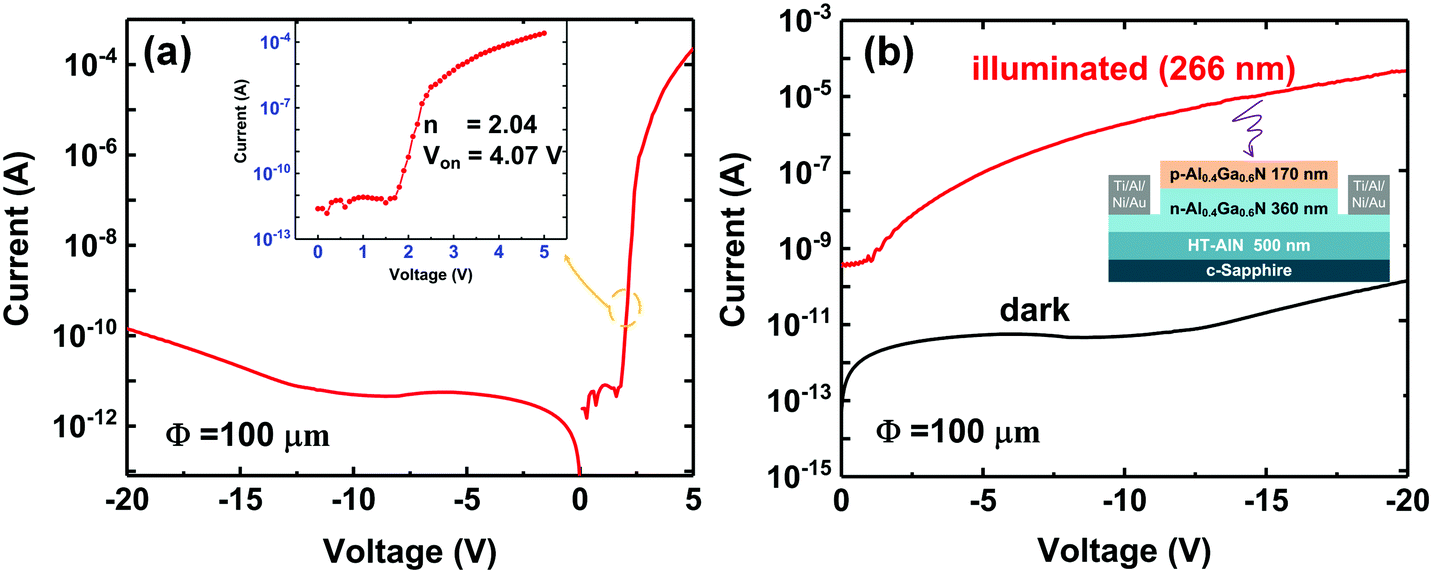 | ||
| Fig. 8 (a) Dark I–V curve of the full Al-rich AlGaN p–n junction diode with the p-type layer grown with the PTGF. (b) Reverse I–V curves of the diode with a mesa diameter of 100 μm under the dark and UV illumination conditions. The insets show the forward I–V curve and the schematic structure of the pn junction. | ||
Moreover, the photoresponse of the AlGaN diodes was also investigated. A DUV light emitting diode with a center wavelength of 266 nm was employed as a light source. The incident optical power density was 220 μW cm−2, as determined by a Newport power meter. Under front UV illumination, the strong photoresponse again verifies that the fabricated AlGaN diodes are pn junctions rather than the Schottky barrier diode formed by the Ni/Au electrode on p-AlGaN, since the photocurrent generated from the depletion region of a zero-biased opaque Schottky contact should be much smaller than that generated from the space-charge region of a pn junction, as in this case (Fig. 8b). The significant photocurrent also indicates the feasibility of the p-AlGaN grown with the PTGF in AlGaN based DUV optoelectronics.
In summary, high doping efficiency has been achieved in Mg-δ-doped Al-rich AlGaN. It was shown by DFT calculations that the Mg substitution is more energetically favorable on the surface of AlGaN, especially for the substitution on the Al site, whereas in the bulk layer the doped Mg prefers to substitute the Ga site. Accordingly, a pulsed TMGa flow was introduced to modify the Mg-doping planes, in which the δ-doping plane can be classified into upper and lower surfaces. In the process of growth, the lower surface is modified by the purge step to increase the Al composition, while the upper surface is modified by the PTGF to impede the upward diffusion of the Mg dopant. Meanwhile, as the epitaxial growth continues, the upper surface is transformed into the bulk of the underlayer with a slightly higher Ga composition by the PTGF, which leads to enhanced Mg incorporation in the bulk. A high hole concentration of 8.3 × 1018 cm−3 was therefore obtained in AlxGa1−xN (x ∼ 0.42) with an average Mg doping concentration of 1.6 × 10¹⁹, indicating a doping efficiency of up to 51.9%. The resistivity is as low as 0.51 Ω cm, comparable to those of the-state-of-art p-GaN. Also, the prepared p-type layer is highly transparent at wavelengths above the absorption edge. The SIMS results show that the Mg incorporation using the proposed method was enhanced by 1.4 times, which can be ascribed to the enhanced Mg substitution for Al by introducing the PTGF at the δ-doping planes and the increased substitution for Ga in the bulk layer. Temperature-dependent Hall measurements indicate a very small EA of ∼26 meV, much lower than the 39 meV of the control sample. The decrease in EA is attributed to the enlarged valence-band bending by the PTGF. Moreover, Al-rich AlGaN pn junctions were fabricated using the p-AlGaN layer grown with the modified doping planes. The resulting pn junctions demonstrate excellent characteristics in terms of leakage current, turn-on voltage, and ideality factor, which proves the applicability of the doping-plane modification concept.
Conflicts of interest
There are no conflicts to declare.Acknowledgements
This work was supported by the National Key R&D Program of China (Grant No. 2016YFB0400901), the State Key Program of National Natural Science Foundation of China (Grant No. 61634002), and Key Realm R&D Program of GuangDong Province (Grant No. 2019B010132004).References
- M. L. Nakarmi, N. Nepal, J. Y. Lin and H. X. Jiang, Appl. Phys. Lett., 2009, 94, 091903 CrossRef.
- K. B. Nam, J. Li, M. L. Nakarmi, J. Y. Lin and H. X. Jiang, Appl. Phys. Lett., 2002, 81, 1038–1040 CrossRef CAS.
- J. P. Zhang, X. Hu, Y. Bilenko, J. Deng, A. Lunev, M. S. Shur, R. Gaska, M. Shatalov, J. W. Yang and M. A. Khan, Appl. Phys. Lett., 2004, 85, 5532–5534 CrossRef CAS.
- Z. G. Shao, D. J. Chen, H. Lu, R. Zhang, D. P. Cao, W. J. Luo, Y. D. Zheng, L. Li and Z. H. Li, IEEE Electron Device Lett., 2014, 35, 372–374 CAS.
- T. Kinoshita, T. Obata, H. Yanagi and S.-I. Inoue, Appl. Phys. Lett., 2013, 102, 012105 CrossRef.
- Z. Jun, T. Wu, W. Feng, Y. Weiyi, X. Hui, D. Jiangnan, F. Yanyan, W. Zhihao and C. Changqing, IEEE Photonics J., 2013, 5, 1600310 Search PubMed.
- J. Simon, V. Protasenko, C. Lian, H. Xing and D. Jena, Science, 2010, 327, 60–64 CrossRef CAS PubMed.
- T. M. Al tahtamouni, J. Y. Lin and H. X. Jiang, AIP Adv., 2014, 4, 047122 CrossRef.
- Y. H. Liang and E. Towe, Appl. Phys. Rev., 2018, 5, 011107 Search PubMed.
- S. R. Jeon, Z. Ren, G. Cui, J. Su, M. Gherasimova, J. Han, H. K. Cho and L. Zhou, Appl. Phys. Lett., 2005, 86, 082107 CrossRef.
- W. Luo, B. Liu, Z. Li, L. Li, Q. Yang, L. Pan, C. Li, D. Zhang, X. Dong, D. Peng, F. Yang and R. Zhang, Appl. Phys. Lett., 2018, 113, 072107 CrossRef.
- M. Martens, C. Kuhn, E. Ziffer, T. Simoneit, V. Kueller, A. Knauer, J. Rass, T. Wernicke, S. Einfeldt, M. Weyers and M. Kneissl, Appl. Phys. Lett., 2016, 108, 151108 CrossRef.
- C. Bayram, J. L. Pau, R. McClintock and M. Razeghi, J. Appl. Phys., 2008, 104, 083512 CrossRef.
- J. Li, W. Yang, S. Li, H. Chen, D. Liu and J. Kang, Appl. Phys. Lett., 2009, 95, 151113 CrossRef.
- J. Tersoff, Phys. Rev. Lett., 1995, 74, 5080–5083 CrossRef CAS PubMed.
- G. Kresse and J. Furthmuller, Phys. Rev. B: Condens. Matter Mater. Phys., 1996, 54, 11169–11186 CrossRef CAS PubMed.
- G. Kresse and J. Furthmüller, Comput. Mater. Sci., 1996, 6, 15–50 CrossRef CAS.
- P. E. Blöchl, Phys. Rev. B: Condens. Matter Mater. Phys., 1994, 50, 17953–17979 CrossRef PubMed.
- J. P. Perdew, K. Burke and M. Ernzerhof, Phys. Rev. Lett., 1996, 77, 3865–3868 CrossRef CAS.
- H. J. Monkhorst and J. D. Pack, Phys. Rev. B: Solid State, 1976, 13, 5188–5192 CrossRef.
- C. G. Van de Walle and J. Neugebauer, J. Appl. Phys., 2004, 95, 3851–3879 CrossRef CAS.
- A. Zoroddu, F. Bernardini, P. Ruggerone and V. Fiorentini, Phys. Rev. B: Condens. Matter Mater. Phys., 2001, 64, 045208 CrossRef.
- B. Lange, C. Freysoldt and J. Neugebauer, Phys. Rev. B: Condens. Matter Mater. Phys., 2010, 81, 2583–2587 Search PubMed.
- Y. Chen, H. Wu, E. Han, G. Yue, Z. Chen, Z. Wu, G. Wang and H. Jiang, Appl. Phys. Lett., 2015, 106, 162102 CrossRef.
- W. J. O.-T., J. Mol. Struct., 1981, 71, 355 CrossRef.
- J. Zhu, F. Liu, G. B. Stringfellow and S. H. Wei, Phys. Rev. Lett., 2010, 105, 195503 CrossRef PubMed.
- E. C. H. Kyle, S. W. Kaun, E. C. Young and J. S. Speck, Appl. Phys. Lett., 2015, 106, 222103 CrossRef.
- Y. Chen, H. Wu, G. Yue, Z. Chen, Z. Zheng, Z. Wu, G. Wang and H. Jiang, Appl. Phys. Express, 2013, 6, 041001 CrossRef.
- D. G. Zhao, Z. S. Liu, J. J. Zhu, S. M. Zhang, D. S. Jiang, H. Yang, J. W. Liang, X. Y. Li and H. M. Gong, Appl. Surf. Sci., 2006, 253, 2452–2455 CrossRef CAS.
- T. Tanaka, A. Watanabe, H. Amano, Y. Kobayashi, I. Akasaki, S. Yamazaki and M. Koike, Appl. Phys. Lett., 1994, 65, 593–594 CrossRef CAS.
- T. Takeuchi, C. Wetzel, S. Yamaguchi, H. Sakai, H. Amano, I. Akasaki, Y. Kaneko, S. Nakagawa, Y. Yamaoka and N. Yamada, Appl. Phys. Lett., 1998, 73, 1691–1693 CrossRef CAS.
- Y. Arakawa, K. Ueno, A. Kobayashi, J. Ohta and H. Fujioka, APL Mater., 2016, 4, 086103 CrossRef.
- B. Sarkar, S. Mita, P. Reddy, A. Klump, F. Kaess, J. Tweedie, I. Bryan, Z. Bryan, R. Kirste, E. Kohn, R. Collazo and Z. Sitar, Appl. Phys. Lett., 2017, 111, 032109 CrossRef.
| This journal is © The Royal Society of Chemistry 2020 |