
 Open Access Article
 This Open Access Article is licensed under a
 Creative Commons Attribution 3.0 Unported Licence
Potential for neutron and proton transmutation doping of GaN and Ga2O3†‡
Julie V.
Logan
 *a,
Elias B.
Frantz
b,
Lilian K.
Casias
c,
Michael P.
Short
a,
Christian P.
Morath
d and
Preston T.
Webster
d
*a,
Elias B.
Frantz
b,
Lilian K.
Casias
c,
Michael P.
Short
a,
Christian P.
Morath
d and
Preston T.
Webster
d
aDepartment of Nuclear Science and Engineering, Massachusetts Institute of Technology, Cambridge, USA. E-mail: jvl2xv@mit.edu
bDepartment of Engineering Science & Mechanics, The Pennsylvania State University, State College, USA
cQuantum Phenomena Division, Sandia National Laboratories, Albuquerque, USA
dSpace Vehicles Directorate, Air Force Research Laboratory, Kirtland Air Force Base, USA
First published on 13th February 2020
Abstract
As the potential applications of GaN and Ga2O3 are limited by the inadequacy of conventional doping techniques, specifically when uniform selective area p-type doping is required, the potential for transmutation doping of these materials is analyzed. All transmuted element concentrations are reported as a function of time for several common proton and neutron radiation sources, showing that previously published results considered a small subset of the dopants produced. A 40 MeV proton accelerator is identified as the most effective transmutation doping source considered, with a 2.25 × 10¹⁷ protons per cm2 fluence yielding net concentrations of uncompensated p-type dopants of 7.7 × 10¹⁵ and 8.1 × 1015 cm−3 for GaN and Ga2O3, respectively. Furthermore, it is shown that high energy proton accelerator spectra are capable of producing dopants required for magnetic and neutron detection applications, although not of the concentrations required for current applications using available irradiation methods.
1 Introduction
Wurtzite GaN and monoclinic β-Ga2O3 are direct wide and ultra-wide bandgap semiconductors with bandgaps of approximately 3.4 and 4.8 eV, respectively. While interest in these two semiconductor systems is growing, the development of some electronic devices using these materials is stalemated by the present inability to achieve selective area p-type doping. Conventional techniques; including selective area etch and regrowth, activation-enhanced laterally pattered ion implantation, and selective area diffusion; have been unable to produce junctions of the required quality for production of high performance vertical GaN transistors.1 This work investigates the potential of transmutation doping as an alternative to circumvent this limitation impeding the use of GaN and Ga2O3 for some applications.GaN has applications in optoelectronic, high-power, and high-frequency devices due to its large breakdown field, high electron mobility, and high converter power density in conjunction with its large heat capacity and thermal conductivity.2 Particular applications include laser diodes, microwave RF power amplifiers, high voltage switching devices, UV photodetectors, Schottky rectifiers, and solar cells.2,3 Interest in Ga2O3 stems from its predicted critical field of 6–8 MV cm−1,4 which is more than double that of GaN and SiC, allowing for high current and voltage (up to 10 kV) power transistor operation. Furthermore, low cost, high quality, scalable melt-grown substrates make Ga2O3 one of the few ultra-wide bandgap materials that is predicted to compete with wide bandgap materials like GaN and SiC for power and RF device applications.4,5
Both GaN and Ga2O3 are also being investigated for use as dilute magnetic semiconductors (DMS) due to these materials' capacity to achieve room temperature ferromagnetism when doped with transition and rare-earth metals. If adequately doped to a few atomic percent, these materials have applications such as spin-based transistors, spin valves, magnetic memories, and spin-polarized light-emitting diodes.6 Examples of applicable transition metal dopants potentially produced from transmutation include Co, Ni, and Cu.7,8 Additionally, proper doping permits use of these materials in more cost-effective and robust thermal neutron detectors. Doping of either of these radiation-tolerant material systems with 6-Li or 10-B permits fabrication of neutron scintillators and semiconductor thermal neutron detectors.2
All electronic device architectures and applications mentioned above require selective semiconductor doping to permit control of carrier concentrations, but in contrast to Si and GaAs, there are not yet well-established, technologically advanced doping methods for wide-bandgap semiconductors.1,4,9 The high bond strength and rigid lattice structure of wide bandgap materials make it difficult to achieve incorporation of substitutional impurities. This makes common doping methods which seek to insert atoms into the lattice through diffusion, implantation, or otherwise, practically demanding. Specifically for GaN, the primary acceptor dopant is Mg and effective p-type doping is difficult because Mg incorporation is complicated, Mg has a large ionization energy of 170–220 eV, and Mg is readily passivated by hydrogen incorporation and nitrogen vacancies.10–13 For Ga2O3, there are no known shallow acceptors and the general consensus in the community is that conventional doping means will not be effective in producing p-type samples.4 Furthermore, producing uniform heavily doped wafers of these materials is limited by the involved nature of the conventional doping methods. However, one feasible method for doping, which is well-suited to permit uniform and selective area doping, has not yet been conclusively explored for these wide bandgap semiconductors: transmutation doping.1
As protons and neutrons move through a semiconductor, they lose energy primarily through elastic or inelastic scattering events with the host nuclei in the case of neutrons and with host nuclei and electrons in the case of protons. Alternatively, these baryons may interact with lattice atoms through nuclear reactions, resulting in the production of excited lattice atom nuclei of a different composition. The decay of these nuclei to lower energy states over time may be associated with the emission of particles (proton(s), neutron(s), electron(s), positron(s)) or high energy gamma rays. This process can result in the production of an atom of a different element within the lattice, doping the semiconductor. The efficiencies of different nuclear reactions and the probabilities of different decays are influenced by the original lattice atom nucleus as well as the energy and identity of the incident particle initiating the reaction.14 Transmutation doping is fundamentally different from implantation doping in that implantation doping relies on injecting a foreign nucleus into the lattice while transmutation doping is the transformation of one native lattice atom into another, the dopant. Transmutation doping is particularly effective for doping as effective dopants typically lie adjacent to the host lattice atom on the periodic table and these are the nuclei which are more likely formed through the decay of excited lattice nuclei.
Neutron and proton transmutation doping are methods capable of producing a high-quality doped semiconductor in terms of doping precision and homogeneity.15,16 Neutron transmutation doped Si has the best quality among all doping methods.17 Dopant concentration precision is achieved because the impurity concentration produced is linearly proportional to the neutron or proton fluence. Precision doping with errors of <1% are readily achievable for neutron transmutation of Si, a well-established process.16,17 Doping precision is important for applications in which highly resistive materials are required, such as avalanche detectors as well as more generally when highly controlled junctions are required as in CMOS fabrication.16,18,19 Both neutron and proton transmutation doping produce more uniform dopant profiles than does ion implantation doping because neutrons and protons both produce dopants along their entire track, in comparison to ion implantation in which dopants are only produced at the end of the incident particle track. Neutron transmutation doping is the most uniform doping mechanism available due to the small probability of a transmutation reaction, the highly penetrating nature of neutrons, the uniformity of neutron flux achievable, and the random isotopic distribution of host nuclei in the sample. Doping uniformity across an entire ingot is achievable.17 Neutron transmutation doped semiconductors do not exhibit the microresistivity structure commonly exhibited by conventionally doped materials. Furthermore, for applications requiring large-scale uniformity, neutron transmutation does not exhibit the doping gradients across the wafer produced by traditional doping methods. For example, float zone doped Si yields slices with four to ten times higher radial resistivity gradient than does neutron transmutation doping.16 This uniformity of doping is important for a variety of devices, but finds its most prominent advantage in high power devices such as thyristors (such as integrated gate-commutated thyristors and gate turn-off thyristors) and insulated-gate bipolar transistors due to the functionality requirements of low on-resistance and high breakdown voltage.17,20 Additionally, the defects generated through neutron transmutation doping can generally be annealed and the dopants activated through relatively low temperature annealing (particularly when compared to ion implantation doping).16,21
Neutron transmutation doping is a method which produces uniform concentrations of impurity atoms in semiconductors and is employed commercially for high power silicon device production.22 There have been no published theoretical or experimental investigations of the potential of transmutation doping of Ga2O3 and, although there have been a few experimental investigations of the potential for the use of thermal neutron transmutation to dope GaN, no effort has conducted a complete analysis considering all impurities introduced due to the irradiation and their temporal variation. In the earliest experimental investigations in 2002 and 2004,23,24 Ge production through (n,γ) reactions with the two stable isotopes of gallium was considered in the interpretation of experimental results. Later, the (n,p) reaction of neutrons with 14-N was included in the analysis after observing that high sample resistivity (108 Ohms at room temperature) was maintained after 1000 °C annealing.25 There exists no analysis including other thermal neutron reactions, fast neutron reactions, or the temporal variation in impurities produced.26,27 Additionally, the use of protons for transmutation doping has not been considered for these wide-bandgap materials. This work addresses all of these shortcomings.
A comprehensive analysis of the fundamental potential for transmutation doping of GaN and Ga2O3, wide bandgap semiconductors, is conducted. All nuclear reactions that produce impurities, their temporal variation, and the potential of non-thermal neutron and proton-induced transmutation are considered. All transmuted elemental concentrations are presented as a function of time following irradiation using a variety of proton and neutron sources, enabling analysis of the use of these techniques for doping to control carrier transport, magnetic properties, and neutron detection capabilities of these materials.
2 Methods
The following neutron and proton transmutation irradiation scenarios are considered: monoenergetic proton irradiation, typical of an accelerator source, of 2, 5, 10, 20, 30, and 40 MeV and neutron irradiation from a variety of potential neutron sources, which are summarized in Table 1. These neutron spectra are visualized in Fig. 1. For all proton spectra, a total fluence of 2.25 × 10¹⁷ protons per cm2 is employed (associated with 1 hour irradiation with a 10 μA accelerator with a 1 cm2 spot size). For all neutron spectra, 3.6 × 10¹⁷ neutrons per cm2 are considered, a fluence associated with 1 hour irradiation in a typical light water reactor of total 1014 neutrons per cm2 per s scalar flux.| Spectrum name | Bins | Spectrum description |
|---|---|---|
| EBR-2 | 29 | Experimental breeder reactor spectrum |
| 252-Cf | 70 | 252-Cf spontaneous fission source |
| BWR-MOX-Gd-40GWd | 1102 | BWR MOX fuel with Gd, 40 GWd per THM |
| PWR-MOX-40GWd | 1102 | PWR MOX fuel with Gd, 40 GWd per THM |
| PWR-UO2-40GWd | 1102 | PWR UO2 fuel, 40 GWd per THM |
| Phenix | 172 | Fast breeder reactor, Phénix |
| ITER-DD | 175 | Magnetic confinement fusion, ITER D-D |
| ITER-DT | 175 | Magnetic confinement fusion, ITER D-T |
| JAEA-FNS | 175 | JAEA fusion neutron source D-T |
| HFIR-highres | 238 | Mat. test reactor, ORNL HFIR midplane |
| All-fast | 3 | 1 MeV neutrons source |
| All-thermal | 3 | 0.025 eV neutron source |
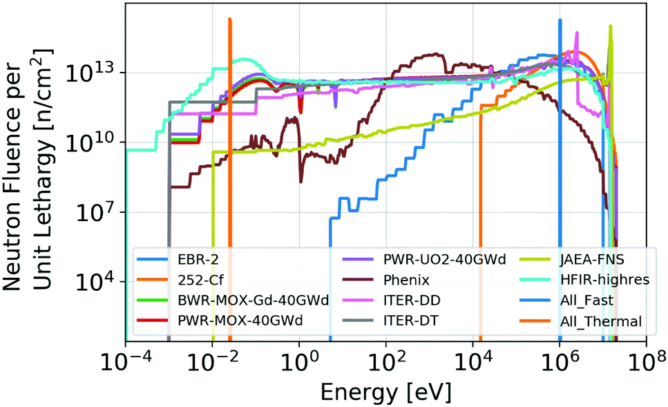 | ||
| Fig. 1 Incident neutron spectra, each of which is used as a source for transmutation quantification. More detail concerning these spectra is included in Table 1. For all neutron spectra shown here, the total fluence of 3.6 × 10¹⁷ neutrons per cm2 is employed (1 hour irradiation in a typical light water reactor of total 1014 neutrons per cm2 per s scalar flux). | ||
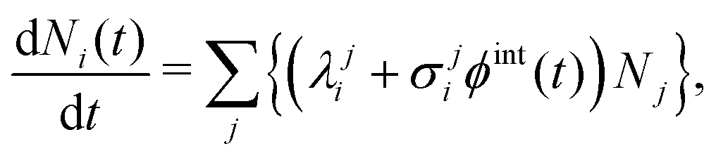
The FISPACT-II enhanced multiphysics inventory and nuclear observables system, a code validated and maintained by the UK Atomic Energy Authority, is utilized to quantify the total elemental transmutation.51 This code computes charged-particle and neutron transmutation and activation using published natural abundances, cross-sections, and decay data, and has previously been validated for semiconductor transmutation applications by comparison to experiments and GEANT4 simulations.52 FISPACT employs the most up-to-date published nuclear data from the TENDL-2017, HEIR-0.1, ENDF/B.VIII.0, JEFF-3.3, JENDL-4.0, and CENDL-3.1 international libraries.51 Specifically for this application, the FISPACT 2017 TENDL database is used for proton (gxs-162) and neutron (gxs-709) nuclear reaction cross-sections, the UKAEDD-12 decay library is used for decay data, and the UKFY-4.1 library (as obtained from JEFF-3.1.1 decay data) is used for fission yields. The use of these nuclear reaction cross-sectional databases implies that input proton and neutron spectra are binned into 162 and 709 equal lethargy bins, respectively.51 It should be noted that, as the published proton cross-section databases do not contain uncertainty quantification for proton reactions, no uncertainties can be derived from this deterministic code. The validity of the results is determined by the accuracy of the cross-section libraries employed.
The nuclear libraries are condensed by FISPACT-II, given the incident radiation spectrum being analyzed. A deterministic, stiff set of coupled ordinary differential rate equations are then solved, the solutions of which provide the time-dependent transmutation of the initial set of nuclides in the sample caused by the input radiation and by spontaneous radioactive decay. The equation governing the concentration, Ni(t) of nuclide i is given in eqn (1) where the summation is conducted over all nuclides.
 | (1) |
In eqn (1), σji [cm2] is the condensed cross-section for production of isotope i from isotope j (a negative value representing destruction equal to the total cross-section for isotope j if i = j), ϕint [cm−2 s−1] is the energy-integrated projectile flux (required due to the use of condensed cross-sections), and λji [s−1] is the decay constant of isotope j to isotope i (a negative value representing destruction equal to the total decay constant for isotope j if i = j).51
3 Results and discussion
3.1 Validation with experiment
To experimentally validate transmuted concentration results in these semiconductors, comparison is made to previous experiment where an unintentionally doped GaN sample was irradiated with thermal and fast neutron fluences each of 1.5 × 10¹⁷ neutrons per cm2 from a thermal neutron pool-type light water moderated and cooled WWR-c reactor, yielding a dopant concentration of 2.2 × 10¹⁶ Ge atoms per cm3.26 As the precise WWR-c neutron spectrum used in the experiment was unavailable, a pure thermal spectrum (0.025 eV) and pure fast spectrum (1 MeV) of the stated fluences and a spectrum from another thermal pool-type light water reactor (LWR) of equivalent total fluence are assumed. Given that both are thermal LWRs and the moderation mechanism is the same for this reactor and that utilized in experiment, one would anticipate that the neutron spectra are similar. The comparison of the computed Ge concentration (from each neutron spectrum) with the experimental 2.2 × 10¹⁶ Ge atoms per cm3 is shown in Fig. 2. As the experimental characterization occurred greater than 3 weeks following irradiation, the concentration is plotted starting at 3 weeks post-irradiation. It is observed that the experimental concentrations fall within the concentrations predicted by this work, which have approximately stabilized during this time interval.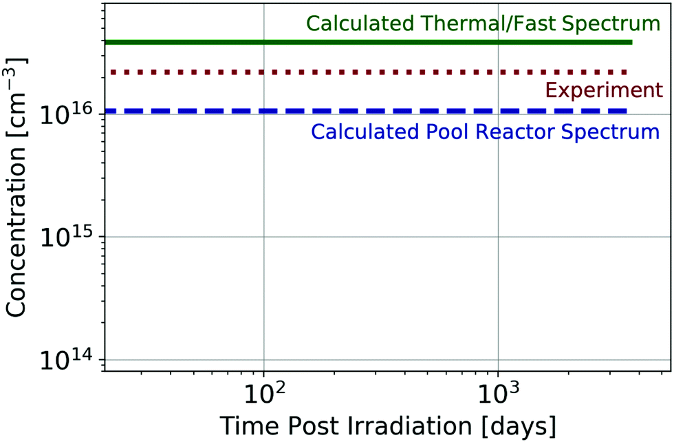 | ||
| Fig. 2 Comparison between experimentally observed26 and computed Ge concentration resulting from GaN neutron irradiation with thermal and fast neutron fluence of 1.5 × 10¹⁷ neutrons per cm2 for pure thermal and pure fast neutron spectra and for a similar thermal pool-type light water reactor as was used for experimental irradiation. Concentrations are shown starting at 3 weeks post-irradiation, as this was when the experiment was performed. | ||
3.2 Temporal transmuted element concentrations
The concentrations of impurities produced as a function of time under proton and neutron irradiation respectively are visualized for GaN in Fig. 3 and 4 and for Ga2O3 in Fig. 5 and 6. It is observed that many additional impurities are produced in concentrations comparable to the historically considered Ge and C.23–27 Additionally, some elemental concentrations show substantial temporal dependence on the order of days to months. This defines the timescale for future experimental study of the doping of these systems through transmutation. It should be noted that these impurities are generally not located on the same site as the parent atom from which they originate due to the subsequent gamma and beta radioactive decays that occur, the energy of which is shared between the emitted particle and the nucleus, causing it to recoil.23 The semiconductor activity (rate of these nuclear decays) as a function of time following irradiation is presented in the ESI.‡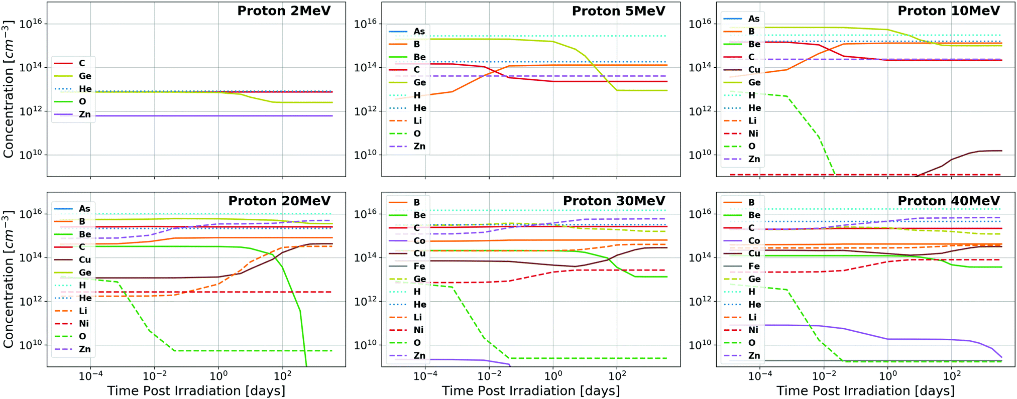 | ||
| Fig. 3 Total concentrations of impurity elements introduced in GaN as a function of time following quasi-monoenergetic 2, 5, 10, 20, 30, and 40 MeV proton irradiation. Substantial dopants of note include Ge, B, C, and Zn for most proton energies (Ep), with the inclusion of Cu, Li, and Ni for Ep ≥ 20 MeV and Be for Ep ≥ 30 MeV. All results are shown in tabular format in the ESI.‡ | ||
 | ||
| Fig. 4 Total concentrations of impurity elements introduced in GaN as a function of time following neutron irradiation, the spectra of which are summarized in Fig. 1. Substantial dopants of note include Ge, B, C, and Zn for most neutron spectra, with the inclusion of Cu and Li in the JAEA-FNS and ITER-DT spectra. The fission power reactor spectra (PWR-UO2-40GWd, BWR-MOX-Gd-40GWd, and PWR-MOX-40GWd) all produce nearly indistinguishable impurity concentration trends and, thus, only the PWR-UO2-40GWd results are visualized. All results are shown in tabular format in the ESI.‡ | ||
 | ||
| Fig. 5 Total concentrations of impurity elements introduced in Ga2O3 as a function of time following quasi-monoenergetic 2, 5, 10, 20, 30, and 40 MeV proton irradiation. Substantial dopants of note include Ge, N, and Zn for most proton energies (Ep), with the inclusion of C for Ep ≥ 10 MeV, Cu and Ni for Ep ≥ 20 MeV, B for Ep ≥ 30 MeV, and Li for Ep ≥ 40 MeV. All results are shown in tabular format in the ESI.‡ | ||
 | ||
| Fig. 6 Total concentrations of impurity elements introduced in Ga2O3 as a function of time following neutron irradiation, the spectra of which are summarized in Fig. 1. Substantial dopants of note include Ge, C, and Zn for most neutron spectra with additional production of Cu and N in JAEA-FNS, ITER-DD, and ITER-DT spectra. The fission power reactor spectra (PWR-UO2-40GWd, BWR-MOX-Gd-40GWd, and PWR-MOX-40GWd) all produce nearly indistinguishable impurity concentration trends and, thus, only the PWR-UO2-40GWd results are visualized. All results are shown in tabular format in the ESI.‡ | ||
3.3 Suitability of transmutation doping for applications
The suitability of neutron and proton irradiation for causing the transmutation required for p-type doping, magnetic applications, and neutron detection applications will now be reviewed.In order to realistically impact semiconductor carrier populations, the compensation of dopants must be considered. As such, the difference between the p-type dopant concentration and the n-type dopant concentration introduced by transmutation is calculated. Many studies used to attribute p-type or n-type character to an impurity consist of density functional theory (DFT) simulations and, while more accurate hybrid functional simulations were chosen when available, there are potential sources of error arising from these simulation sources. Furthermore, the following assumptions are made: all dopants reside on their parent sublattice site (no interstitial or antisite defects) and the crystal is fully annealed (no radiation-induced compensating self-interstitials or vacancies). Deep levels are included in n- or p-type attribution because their effective depth is Fermi level dependent, their depth may be overestimated in the DFT results, and because they are still employed to control semiconductor electrical conductivity (for example Fe in Ga2O3 producing a semi-insulating material4). Despite the potential sources of error in this attribution, Fig. 3–6 can be used to generate net doping introduced as a function of time for one's specific application. This attribution may be irradiation scenario dependent, as different amounts of damage and annealing can impact the site upon which the transmuted elements reside, which impacts their energy level and their resulting doping character. The dominant source of error in this attribution is likely the assumed position of the impurities within the lattice. With all of these potential sources of error in mind, the attributions used in this analysis of GaN and Ga2O3 doping are contained in Tables 2 and 3 respectively.
| Type | Attribution notes | |
|---|---|---|
| H | — | Complex form determines nature28 |
| He | — | |
| Li | p | Deep acceptor 2.23 eV29 |
| Be | p | Predicted 0.060 eV,30,31 but deep acceptor 2.16 eV |
| Observed,29,32 reduces p-type Mg depth to 0.170 eV33 | ||
| B | — | No sources available |
| C | p | Deep acceptor 0.9 eV (DFT), 1 eV (experiment)34–36 |
| O | n | Shallow donor on N, acceptor on interstitial or OGa site37 |
| Fe | p | Deep acceptor 3.17 eV38–41 |
| Co | — | No sources available |
| Ni | p | Activates Mg (p-type) dopants (H desorption)42 |
| Cu | p | Deep acceptor 2.4 eV, p-type observed43–45 |
| Zn | p | Deep acceptor 0.364 eV (DFT), 0.34 eV (experiment)46 |
| Ge | n | Shallow donor 0.03 eV28 |
| As | n | Deep donor 2.6–2.7 eV47–50 |
| Type | Attribution notes | |
|---|---|---|
| H | — | Complex form determines nature28 |
| He | — | No sources available |
| Li | p | Deep acceptor 1.6–1.9 eV53 |
| Be | p | Deep acceptor54 |
| B | — | No sources available |
| C | p | Deep acceptor >2 eV4,55,56 |
| N | p | Deep acceptor 1.33 eV57 |
| F | n | Shallow donor58 |
| Fe | p | Deep acceptor 3.9–4.0 eV59,60 |
| Co | — | Deep acceptor >2 eV4,55,56 |
| Ni | p | Deep acceptor 0.76 eV54 |
| Cu | p | Deep acceptor 0.96 eV54,61,62 |
| Zn | p | Deep acceptor 0.33 eV (DFT), <0.5 eV (experiment)54,63,64 |
| Ge | n | Shallow donor 0.01–0.03 eV60,65 |
| As | — | No sources available |
Impurities produced in transmutation are binned using Tables 2 and 3 to produce the total n- and p-type concentration of impurities introduced as a function of time, as shown for proton and neutron irradiation spectra respectively in Tables 4 and 5 for GaN and in Tables 6 and 7 for Ga2O3 at 50 days post one hour irradiation. It is observed that the samples become bulk n-type or are approximately compensated for the majority of irradiation scenarios. The full temporal variability is presented in the ESI.‡ Exceptions in which net dominant p-type doping is observed exist for GaN and Ga2O3 when irradiated with JAEA-FNS neutrons (a D-T fusion neutron source), 252-Cf neutrons (spontaneous fission) or protons of 2, 5, 20, 30, and 40 MeV. This trend of increasing p-type doping with increasing proton energy occurs because the probabilities of proton interactions generally peak at 10x MeV where x is the number of neutrons emitted from the unstable nucleus through the (p, xn) reaction.52 Because of this, higher energy protons will be more likely to form a nucleus with a proton to neutron ratio that is too high to be stable. This will result in subsequent β+ decay, which converts protons to neutrons and produces lower atomic number elements. These elements will likely contribute to p-type doping by acting as acceptors relative to the parent nucleus.
| Source | Induced dopant concentration in GaN [cm−3] | ||
|---|---|---|---|
| p-Type | n-Type | Net p-type | |
| P-2MeV | 8.4 × 10¹² | 2.6 × 10¹² | 5.7 × 10¹² |
| P-5MeV | 6.4 × 10¹³ | 2.5 × 10¹³ | 3.9 × 10¹³ |
| P-10MeV | 4.6 × 10¹⁴ | 1.1 × 10¹⁵ | −6.0 × 10¹⁴ |
| P-20MeV | 6.7 × 10¹⁵ | 5.2 × 10¹⁵ | 1.5 × 10¹⁵ |
| P-30MeV | 9.0 × 10¹⁵ | 2.0 × 10¹⁵ | 7.0 × 10¹⁵ |
| P-40MeV | 9.4 × 10¹⁵ | 1.7 × 10¹⁵ | 7.7 × 10¹⁵ |
| Source | Induced dopant concentration in GaN [cm−3] | ||
|---|---|---|---|
| p-Type | n-Type | Net p-type | |
| EBR-2 | 3.8 × 10¹⁴ | 6.7 × 10¹⁴ | −2.9 × 10¹⁴ |
| 252-Cf | 6.5 × 10¹⁴ | 2.4 × 10¹⁴ | 4.1 × 10¹⁴ |
| BWR-MOX-Gd-40GWd | 1.6 × 10¹⁵ | 1.3 × 10¹⁶ | −1.1 × 10¹⁶ |
| PWR-MOX-40GWd | 1.4 × 10¹⁵ | 1.3 × 10¹⁶ | −1.1 × 10¹⁶ |
| PWR-UO2-40GWd | 2.3 × 10¹⁵ | 1.4 × 10¹⁶ | −1.1 × 10¹⁶ |
| Phenix | 1.9 × 10¹⁴ | 2.6 × 10¹⁶ | −2.6 × 10¹⁶ |
| ITER-DD | 8.9 × 10¹⁴ | 6.3 × 10¹⁵ | −5.4 × 10¹⁵ |
| ITER-DT | 3.6 × 10¹⁵ | 1.2 × 10¹⁶ | −8.1 × 10¹⁵ |
| JAEA-FNS | 1.1 × 10¹⁶ | 6.1 × 10¹⁵ | 5.1 × 10¹⁵ |
| HFIR-highres | 1.2 × 10¹⁶ | 2.6 × 10¹⁶ | −1.4 × 10¹⁶ |
| All-fast | 2.9 × 10¹⁴ | 2.6 × 10¹⁴ | 2.6 × 10¹³ |
| All-thermal | 2.9 × 10¹⁶ | 4.6 × 10¹⁶ | −1.7 × 10¹⁶ |
| Source | Induced dopant concentration in Ga2O3 [cm−3] | ||
|---|---|---|---|
| p-Type | n-Type | Net p-type | |
| P-2MeV | 6.2 × 10¹² | 2.3 × 10¹² | 3.9 × 10¹² |
| P-5MeV | 4.2 × 10¹³ | 2.1 × 10¹³ | 2.1 × 10¹³ |
| P-10MeV | 9.3 × 10¹⁴ | 9.0 × 10¹⁴ | 3.4 × 10¹³ |
| P-20MeV | 7.6 × 10¹⁵ | 4.5 × 10¹⁵ | 3.1 × 10¹⁵ |
| P-30MeV | 9.5 × 10¹⁵ | 1.7 × 10¹⁵ | 7.8 × 10¹⁵ |
| P-40MeV | 9.6 × 10¹⁵ | 1.4 × 10¹⁵ | 8.1 × 10¹⁵ |
| Source | Induced dopant concentration in Ga2O3 [cm−3] | ||
|---|---|---|---|
| p-Type | n-Type | Net p-type | |
| EBR-2 | 4.9 × 10¹³ | 5.7 × 10¹⁴ | −5.2 × 10¹⁴ |
| 252-Cf | 2.9 × 10¹⁴ | 2.1 × 10¹⁴ | 8.4 × 10¹³ |
| BWR-MOX-Gd-40GWd | 1.2 × 10¹⁴ | 1.1 × 10¹⁶ | −1.1 × 10¹⁶ |
| PWR-MOX-40GWd | 1.2 × 10¹⁴ | 1.1 × 10¹⁶ | −1.1 × 10¹⁶ |
| PWR-UO2-40GWd | 1.2 × 10¹⁴ | 1.2 × 10¹⁶ | −1.1 × 10¹⁶ |
| Phenix | 4.4 × 10¹³ | 2.2 × 10¹⁶ | −2.2 × 10¹⁶ |
| ITER-DD | 9.3 × 10¹³ | 5.4 × 10¹⁵ | −5.3 × 10¹⁵ |
| ITER-DT | 2.7 × 10¹⁵ | 1.0 × 10¹⁶ | −7.4 × 10¹⁵ |
| JAEA-FNS | 1.4 × 10¹⁶ | 5.2 × 10¹⁵ | 8.6 × 10¹⁵ |
| HFIR-highres | 1.2 × 10¹⁴ | 2.2 × 10¹⁶ | −2.2 × 10¹⁶ |
| All-fast | 1.3 × 10¹² | 2.3 × 10¹⁴ | −2.2 × 10¹⁴ |
| All-thermal | 1.9 × 10¹⁴ | 3.9 × 10¹⁶ | −3.9 × 10¹⁶ |
It should be noted that the neutron fluence employed in this computation (3.6 × 10¹⁷ neutrons per cm2) was chosen with reactor fluxes in mind, which is unrealistic for current accelerator-based D-T generators, which would require over 100 hours of continuous operation to achieve this fluence.66,67 For a 252-Cf source of 10 grams, 55 hours of continuous irradiation at a distance of 1 cm would be required.68 The dopant population becomes more p-type as a function of time as the dominant n-type dopant Ge decays. Originally, the Ge isotopes 68-Ge, 69-Ge, and 70-Ge are produced in approximately equal amounts and 69-Ge decays to stable 69-Ga through β+ decay with a half-life of 1.63 days, thus reducing the n-type dopant concentration. Additionally, the p-type dopant concentration is increased due to production of 67-Zn through the electron capture decay of 67-Ga with a half-life of 3.26 days. This temporal variability of electrical properties illustrates the importance of a holistic analysis when considering transmutation doping.
As mentioned in Section 1, transition metal doping of GaN and Ga2O3 can lead to room temperature ferromagnetism. Specifically in Fig. 3 and 4 it is observed that long-lived Fe, Co, Ni, and Cu are produced in GaN due to transmutation. For proton irradiation of 20 MeV and above, concentrations of >1012 cm−3 and >1013 cm−3 of Ni and Cu respectively are produced per hour. Neutrons are less effective at causing transition metal doping with the primary irradiations of note being the two D-T fusion sources producing Cu concentrations of >1012 cm−3. Similar results are observed in Fig. 5 and 6 for Ga2O3, due to the fact that the transmuted metallic constituents derive from the Ga present in both semiconductors. Given current applications, this doping efficiency is insufficient to provide the few atomic percent mole fractions required to produce DMS.6–8
Many neutron detection applications rely primarily on the large cross-section of interaction for neutrons with 10-B and 6-Li.69 It is observed that protons are efficient at producing these two isotopes in GaN and Ga2O3. As both of these isotopes are radioactively stable, their concentration is invariant with time after they are produced. It is found that in GaN, protons with energies >30 MeV are capable of producing concentrations of >1014 cm−3 of 6-Li and 10-B per hour of irradiation. In Ga2O3, concentrations only exceed 1012 cm−3 for B-10 from 40 MeV protons. This difference arises because 10-B and 6-Li are transmuted from the anion, which is not common between the two semiconductors. The uniform production of neutron-sensitive isotopes through transmutation is desirable because the neutron reaction products must travel to and deposit energy in the active region of the detector, a requirement which sets an intrinsic limit to the efficiency of a 6-Li or 10-B coated semiconductor detectors to 4.5%.70 Despite this, the concentrations produced through transmutation are unsuitable for thermal neutron detection applications as they result in intrinsic detection efficiencies, given an assumed 1 cm thick absorber layer, of <0.001%.
4 Conclusion
The potential for transmutation doping of GaN and Ga2O3 is presented, as unresolved doping difficulties restrict the use of these materials, specifically when p-type doping is required. All transmuted element concentrations are reported as a function of time, showing the substantial temporal variability of the semiconductor composition. A range of realistically obtainable proton and neutron spectra are considered, as originating from accelerators, fission reactors, fusion reactors and reactions, and radioactive isotopes. It is shown that, for the impurity attribution considered in this analysis, most proton spectra as well as 252-Cf spontaneous fission and D-T fusion neutron spectra are capable of producing a net increase in p-type dopants which increases with time as Ge decays and Zn is produced. At 50 days following a one hour irradiation, the net concentration of uncompensated p-type dopants introduced is 7.7 × 10¹⁵ and 8.1 × 1015 cm−3 for GaN and Ga2O3 respectively for the most effective irradiation considered (40 MeV protons). Furthermore, it is shown that high energy proton accelerator spectra are capable of producing Cu, a key dopant for magnetic applications, in concentrations of >1013 cm−3 per hour in both semiconductors, but this efficiency is orders of magnitude too small to effectively produce dilute magnetic semiconductors. Finally, concentrations of >1014 cm−3 of key neutron detection isotopes are produced in GaN per hour through similar high energy proton irradiation, but these concentrations are again too small for current neutron detector implementations.Conflicts of interest
There are no conflicts to declare.Acknowledgements
The present work has benefited from the financial support of the US Department of Defense SMART Fellowship.Notes and references
- I. C. Kizilyalli, E. P. Carlson, D. W. Cunningham, J. S. Manser, Y. Xu and A. Y. Liu, Wide Band-Gap Semiconductor Based Power Electronics for Energy Efficiency, 2018, pp. 1–17 Search PubMed.
- C. Zhou, A. Ghods, V. G. Saravade, P. V. Patel, K. L. Yunghans, C. Ferguson, Y. Feng, B. Kucukgok, N. Lu and I. T. Ferguson, ECS J. Solid State Sci. Technol., 2017, 6, Q149–Q156 CrossRef CAS.
- K. N. Chopra, Lat. Am. J. Phys. Educ., 2014, 8, 541–547 Search PubMed.
- M. Tadjer, J. L. Lyons, N. Nepal, J. A. Freitas, A. D. Koehler and G. M. Foster, ECS J. Solid State Sci. Technol., 2019, 8, Q3187–Q3194 CrossRef.
- Z. Galazka, Semicond. Sci. Technol., 2018, 33, 113001 CrossRef.
- S. A. Chambers and B. Gallagher, New J. Phys., 2008, 10, 055004 CrossRef.
- P. R. Ganz, C. Sürgers, G. Fischer and D. M. Schaadt, J. Phys.: Conf. Ser., 2010, 200, 062006 CrossRef.
- M. Shakil, A. Husain, M. Zafar, S. Ahmad, M. Khan, M. Masood and A. Majid, Chin. J. Phys., 2018, 56, 1570–1577 CrossRef CAS.
- M. G. Pravica, N. A. Guardala and J. L. Price, Diamond Relat. Mater., 2009, 18, 846–849 CrossRef CAS.
- J. K. Sheu and G. C. Chi, J. Phys.: Condens. Matter, 2002, 14, R657–R702 CrossRef CAS.
- Y.-T. Shi, F.-F. Ren, W.-Z. Xu, X. Chen, J. Ye, L. Li, D. Zhou, R. Zhang, Y. Zheng, H. H. Tan, C. Jagadish and H. Lu, Sci. Rep., 2019, 9, 8796 CrossRef PubMed.
- M. Tadjer, B. Feigelson, J. Greenlee, J. A. Freitas, T. J. Anderson, J. Hite, L. Ruppalt, C. R. Eddy, K. Hobart and F. J. Kub, ECS J. Solid State Sci. Technol., 2016, 5, P124–P127 CrossRef CAS.
- J. Chen, W. Yi, T. Kimura, S. Takashima, M. Edo and T. Sekiguchi, Appl. Phys. Express, 2019, 12, 051010 CrossRef CAS.
- K. Krane, Introductory Nuclear Physics, Wiley, 1987 Search PubMed.
- S. Kang and H. Cho, Method for doping gallium Nitride (GaN) substrates and the resulting doped gan substrate, 2002.
- J. M. Meese, in The NTD Process – A New Reactor Technology, ed. J. M. Meese, Springer US, Boston, MA, 1979, pp. 1–10 Search PubMed.
- M. Kim, S. Park and I. Lim, 2009 13th European Conference on Power Electronics and Applications, 2009, pp. 1–10.
- S. H. Park, T. W. Kang and T. W. Kim, J. Mater. Sci., 2004, 39, 3217–3219 CrossRef CAS.
- J. Montserrat, J. Bausells, E. Lora-Tamayo and F. Serra-Mestres, Vacuum, 1989, 39, 687–690 CrossRef CAS.
- J. W. Cleland, K. Lark-Horovitz and J. C. Pigg, Phys. Rev., 1950, 78, 814–815 CrossRef CAS.
- S. H. Park, T. W. Kang and T. W. Kim, J. Mater. Sci., 2004, 39, 6353–6355 CrossRef CAS.
- S. B. Duun, A. B. Nielsen, C. Hendrichsen, T. Sveigaard, O. T. Andersen, J. J. Jabłoński and L. A. Jensen, Neutron Transmutation Doped (NTD) Silicon for High Power Electronics, Topsil Semiconductor Materials, 2013.
- K. Kuriyama, T. Tokumasu, J. Takahashi, H. Kondo and M. Okada, Appl. Phys. Lett., 2002, 80, 3328–3330 CrossRef CAS.
- K. Kuriyama, T. Tokumasu, H. Sano and M. Okada, Solid State Commun., 2004, 131, 31–35 CrossRef CAS.
- T. Nakamura, K. Kamioka, K. Kuriyama, K. Kushida, Q. Xu and M. Hasegawa, Solid State Commun., 2015, 205, 1–3 CrossRef CAS.
- A. Y. Polyakov, N. B. Smirnov, A. V. Govorkov, N. G. Kolin, D. I. Merkurisov, V. M. Boiko, A. V. Korulin and S. J. Pearton, J. Vac. Sci. Technol., B: Nanotechnol. Microelectron.: Mater., Process., Meas., Phenom., 2010, 28, 608–612 CAS.
- S. Park, T. Kang and T. W. Kim, J. Mater. Sci., 2004, 39, 6353–6355 CrossRef CAS.
- M. Reshchikov and H. Morkoç, J. Appl. Phys., 2005, 97, 061301 CrossRef.
- J. Pankove, M. Duffy, E. Miller and J. Berkeyheiser, J. Lumin., 1973, 8, 89–93 CrossRef CAS.
- F. Bernardini, V. Fiorentini and A. Bosin, Appl. Phys. Lett., 1997, 70, 2990–2992 CrossRef CAS.
- Y. Nakano and T. Jimbo, Appl. Phys. Lett., 2002, 81, 3990–3992 CrossRef CAS.
- F. Albrecht, U. Reislöhner, G. Pasold, C. Hülsen, W. Witthuhn, J. Grillenberger and M. Dietrich, Appl. Phys. Lett., 2004, 84, 3876–3878 CrossRef CAS.
- C.-C. Yu, C.-F. Chu, J.-Y. Tsai, C.-F. Lin, W.-H. Lan, C.-I. Chiang and S.-C. Wang, Jpn. J. Appl. Phys., 2001, 40, L417–L419 CrossRef CAS.
- J. Hu, Y. Zhang, M. Sun, D. Piedra, N. Chowdhury and T. Palacios, Mater. Sci. Semicond. Process., 2018, 78, 75–84 CrossRef CAS.
- L. Li, J. Yu, Z. Hao, L. Wang, J. Wang, Y. Han, H. Li, B. Xiong, C. Sun and Y. Luo, Comput. Mater. Sci., 2017, 129, 49–54 CrossRef CAS.
- J. L. Lyons, A. Janotti and C. G. Van de Walle, Phys. Rev. B: Condens. Matter Mater. Phys., 2014, 89, 035204 CrossRef.
- A. F. Wright, J. Appl. Phys., 2005, 98, 103531 CrossRef.
- S. Heikman, S. Keller, T. Mates, S. DenBaars and U. Mishra, J. Cryst. Grow., 2003, 248, 513–517 CrossRef CAS.
- R. Heitz, P. Maxim, L. Eckey, P. Thurian, A. Hoffmann, I. Broser, K. Pressel and B. K. Meyer, Phys. Rev. B: Condens. Matter Mater. Phys., 1997, 55, 4382–4387 CrossRef CAS.
- M. Iwinska, R. Piotrzkowski, E. Litwin-Staszewska, T. Sochacki, M. Amilusik, M. Fijalkowski, B. Lucznik and M. Bockowski, Appl. Phys. Express, 2016, 10, 011003 CrossRef.
- J. L. Lyons, A. Janotti and C. G. Van de Walle, Phys. Rev. B: Condens. Matter Mater. Phys., 2014, 89, 035204 CrossRef.
- I. Waki, H. Fujioka, M. Oshima, H. Miki and M. Okuyama, J. Cryst. Grow., 2002, 234, 459–462 CrossRef CAS.
- J. Senawiratne, M. Strassburg, A. Payne, A. Asghar, W. Fenwick, N. Li, I. Ferguson and N. Dietz, MRS Online Proc. Libr., 2005, 892, 0892-FF23-08 CrossRef.
- K. Yohannes and D.-H. Kuo, Mater. Sci. Semicond. Process., 2015, 29, 288–293 CrossRef CAS.
- S. W. Kim, Y. H. Park, I. Kim, T.-E. Park, B. W. Kwon, W. K. Choi and H.-J. Choi, Nanoscale, 2013, 5, 8550–8554 RSC.
- S. Fischer, C. Wetzel, E. E. Haller and B. K. Meyer, Appl. Phys. Lett., 1995, 67, 1298–1300 CrossRef CAS.
- C. G. Van de Walle and J. Neugebauer, Appl. Phys. Lett., 2000, 76, 1009–1011 CrossRef CAS.
- J. I. Pankove and J. A. Hutchby, J. Appl. Phys., 1976, 47, 5387–5390 CrossRef CAS.
- L. J. Guido, P. Mitev, M. Gherasimova and B. Gaffey, Appl. Phys. Lett., 1998, 72, 2005–2007 CrossRef CAS.
- X. Li, S. Kim, E. E. Reuter, S. G. Bishop and J. J. Coleman, Appl. Phys. Lett., 1998, 72, 1990–1992 CrossRef CAS.
- J.-C. Sublet, The FISPACT-II User Manual, 2015 Search PubMed.
- J. V. Logan, M. P. Short, P. T. Webster, C. P. Morath and E. H. Steenbergen, J. Mater. Chem. C, 2019, 7, 8905–8914 RSC.
- A. Kyrtsos, M. Matsubara and E. Bellotti, Appl. Phys. Lett., 2018, 112, 032108 CrossRef.
- C. Tang, J. Sun, N. Lin, Z. Jia, W. Mu, X. Tao and X. Zhao, RSC Adv., 2016, 6, 78322–78334 RSC.
- J. L. Lyons, D. Steiauf, A. Janotti and C. G. Van de Walle, Phys. Rev. Appl., 2014, 2, 064005 CrossRef.
- S. Lany, APL Mater., 2018, 6, 046103 CrossRef.
- L. Dong, R. Jia, C. Li, B. Xin and Y. Zhang, J. Alloys Compd., 2017, 712, 379–385 CrossRef CAS.
- J. Yan and C. Qu, J. Semicond., 2016, 37, 042002 CrossRef.
- M. E. Ingebrigtsen, J. B. Varley, A. Y. Kuznetsov, B. G. Svensson, G. Alfieri, A. Mihaila, U. Badstübner and L. Vines, Appl. Phys. Lett., 2018, 112, 042104 CrossRef.
- A. T. Neal, S. Mou, S. Rafique, H. Zhao, E. Ahmadi, J. S. Speck, K. T. Stevens, J. D. Blevins, D. B. Thomson, N. Moser, K. D. Chabak and G. H. Jessen, Appl. Phys. Lett., 2018, 113, 062101 CrossRef.
- C. Zhang, F. Liao, X. Liang, H. Gong, Q. Liu, L. Li, X. Qin, X. Huang and C. Huang, Phys. B, 2019, 562, 124–130 CrossRef CAS.
- Y. Zhang, J. Yan, Q. Li, C. Qu, L. Zhang and W. Xie, Mater. Sci. Eng., B, 2011, 176, 846–849 CrossRef CAS.
- X. Wang, F. Zhang, K. Saito, T. Tanaka, M. Nishio and Q. Guo, J. Phys. Chem. Solids, 2014, 75, 1201–1204 CrossRef CAS.
- X. Wang, F. Zhang, K. Saito, T. Tanaka, M. Nishio and Q. Guo, J. Phys. Chem. Solids, 2014, 75, 1201–1204 CrossRef CAS.
- J. B. Varley, J. R. Weber, A. Janotti and C. G. Van de Walle, Appl. Phys. Lett., 2010, 97, 142106 CrossRef.
- C. Konno, K. Ochiai, M. Wada and S. Sato, Fusion Eng. Des., 2008, 83, 1774–1781 CrossRef CAS.
- A. Klix, T. DÖring, A. R. Domula and K. Zuber, EPJ Web Conf., 2018, 170, 02004 CrossRef.
- R. Radev and T. McLean, Neutron Sources for Standard-Based Testing, Department of Energy Technical Report, 2014.
- G. Knoll, Radiation Detection and Measurement, Wiley, 2000, pp. 505–522 Search PubMed.
- D. McGregor, M. Hammig, Y.-H. Yang, H. Gersch and R. Klann, Nucl. Instrum. Methods Phys. Res., Sect. A, 2003, 500, 272–308 CrossRef CAS.
Footnotes |
| † All data, scripts, and intermediate analysis files can be found on our GitHub repository for this manuscript https://github.com/jvl2xv/GaN_Ga2O3_TransmutationDoping. See DOI: http://10.5281/zenodo.3462165 |
| ‡ Electronic supplementary information (ESI) available. See DOI: 10.1039/d0ma00017e |
| This journal is © The Royal Society of Chemistry 2020 |