
 Open Access Article
 This Open Access Article is licensed under a
 Creative Commons Attribution 3.0 Unported Licence
A simple method for production of hydrophilic, rigid, and sterilized multi-layer 3D integrated polydimethylsiloxane microfluidic chips†
Tomoko Gowa
Oyama
 *,
Kotaro
Oyama
and
Mitsumasa
Taguchi
*,
Kotaro
Oyama
and
Mitsumasa
Taguchi
Quantum Beam Science Research Directorate, National Institutes for Quantum and Radiological Science and Technology (QST), 1233 Watanuki-machi, Takasaki-shi, Gunma 370-1292, Japan. E-mail: ohyama.tomoko@qst.go.jp
First published on 28th May 2020
Abstract
Polydimethylsiloxane (PDMS) has many desirable features for microfluidics applications, particularly in diagnostics and pharmaceuticals, but its hydrophobicity and the lack of a practical method for bonding PDMS layers limit its use. Moreover, the flexibility of PDMS causes unwanted deformation during use in some applications. Here, we report a simple method for solving these problems simultaneously using an electron beam (EB) or γ-rays, which are commonly used for sterilizing medical products. Simply by applying EB or γ-ray irradiation to stacked PDMS layers, we can not only bond the interfaces between the layers by forming Si–O–Si covalent bonds but also achieve long-lasting hydrophilization and sterilization of the internal microchannels and chambers, prevent nonspecific adsorption and absorption of hydrophobic small molecules, and enhance the mechanical strength of the material by converting bulk PDMS into a Si–Ox-rich (where x is 3 or 4) structure though crosslinking. Unlike the one-at-a-time plasma process, EBs and γ-rays can penetrate through many stacked layers of PDMS sealed in their final package, enabling batch modification and bonding. The method requires no chemical crosslinkers, adhesive agents, or fillers; hence, it does not undermine the advantages of PDMS such as ease of molding in soft lithography, biocompatibility, and optical transparency. Furthermore, bonding is achieved with high-throughput yield because it occurs after re-adjustable alignment. We demonstrate that this method is applicable in the mass production of 3D integrated PDMS microfluidic chips with some glass-like properties as well as for 3D structures with complex shapes that are difficult to fabricate with plastic or glass.
Introduction
Polydimethylsiloxane (PDMS) is most commonly used as a base material in microfluidic chips, particularly for proof-of-concept purposes in the academic community.1–5 PDMS has properties analogous to glass, such as biological inertness and optical transparency, while additionally enabling the quick and easy fabrication of devices at low cost.1,5 However, for mass production of the devices and for practical applications, particularly in diagnostics and drug development, it is necessary to overcome the two major drawbacks of PDMS: its hydrophobicity and the lack of a practical method for bonding PDMS layers. Because of its hydrophobicity (water contact angle, WCA: ∼110°), PDMS not only repels aqueous solutions but also absorbs and/or adsorbs hydrophobic small molecules such as amino acids, growth factors, and drugs.1,2 The method for bonding PDMS layers is a critical issue not only for the creation of a leak-proof seal between the microfluidic device and the substrate but also for realizing 3D integrated microfluidic chips which have attracted much attention for their increasing accuracy and functionality.1,5–10 Only a few functions can be realized in a one-layer microfluidic device, but when layers having different microfeatures are integrated, multiple functions can be implemented with one chip: a single 3D microfluidic chip is equivalent to many conventional one-layer devices, and the ability to conduct repeated mixing, sorting, and separation in one 3D chip increases the accuracy of these functions. In addition to the hydrophobicity and lack of a practical bonding method, the flexibility of PDMS, which facilitates demolding during fabrication and expands its application to wearable devices, becomes disadvantageous during use in some cases; the pressure-induced deformation of PDMS microchannels generates untargeted flow velocity and a pressure drop.3,4Extensive efforts have been made to provide PDMS with hydrophilicity and rigidity. A common modification method is plasma irradiation, which can change the hydrophobic methyl groups (Si–CH3) into hydrophilic silanol groups (Si–OH) and produce a Si–Ox-rich (where x is 3 or 4) hard layer on the surface.11 However, the PDMS recovers its original hydrophobicity within minutes because the modified thin surface layer (less than a few hundreds of nanometers thick11) is easily exchanged for unmodified bulk because of the high mobility of molecular chains, which is associated with the low glass-transition temperature of PDMS (Tg ≲ −120 °C).12 Alternative methods have been proposed for achieving longer-lasting modification, such as chemical coating12,13 and the use of low-energy electron beams (LE-EB).14 Although our group previously showed that a 55 kV LE-EB produces a Si–Ox-rich layer as thick as ∼40 μm on the PDMS surface that can prolong the hydrophilicity for more than five months,14 the effect does not reach the bulk. The dissimilar mechanical properties of the modified surface layer and of the unmodified bulk underneath can result in unwanted cracking and warping in the substrate.11,14
Like hydrophilization and hardening of PDMS surfaces, bonding also commonly uses plasma: both surfaces of the PDMS layers are activated by plasma and immediately put into contact to form covalent Si–O–Si bonds between the surfaces.6 The main difficulty of this technique is the necessity of achieving precise alignment on the first try without subsequent adjustment, since the layers are irreversibly bonded once contact is made between the surfaces. Several plasma-free methods have also been proposed and generally involve controlling the mixing ratio of curing agents and/or optimizing curing processes.7,8,10 These bonding methods by plasma or curing only require simple equipment; hence, they are easily accessible for the academic community and suitable for proof-of-concept purposes. However, there is still room for improvement in terms of throughput. In addition, these existing bonding methods require additional treatments for hydrophilization and enhancement of robustness.
In this study, we introduce a simple method that can solve all of the above problems relating to the modification and bonding of PDMS simultaneously: irradiation of the PDMS with an electron beam (EB) or 60Co γ-rays, which are used in commercial facilities to sterilize medical products.15 These forms of ionizing radiation can penetrate through many stacked PDMS layers and simultaneously enable (i) bonding of the interfaces between the multiple layers, (ii) reinforcement of mechanical strength while maintaining optical transparency, (iii) long-lasting hydrophilization, (iv) sterilization of internal microchannels and chambers, and (v) suppression of the absorption and/or adsorption of small molecules (Fig. 1). With this method, 3D integrated microfluidic chips having some glass-like properties can be realized using single-layer PDMS devices prepared by classic soft lithography. The proposed method can be used to transfer the technologies developed in academia to industry owing to its mass-production capability.
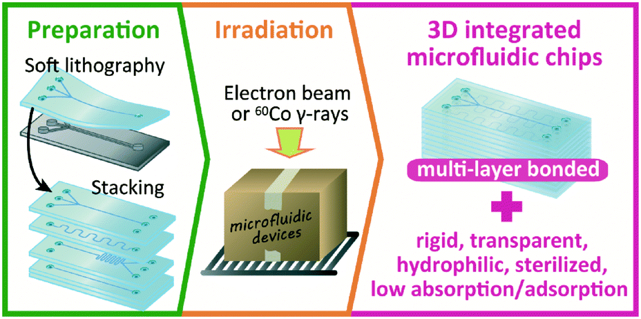 | ||
| Fig. 1 Schematic of proposed method for production of 3D integrated polydimethylsiloxane (PDMS) microfluidic chips having a variety of advantages by simple irradiation with an electron beam or 60Co γ-rays. | ||
This paper describes the effects of EB and γ-ray irradiation on PDMS in terms of compressive modulus, optical transparency, WCA, and absorption/adsorption levels of hydrophobic small molecules. The results obtained are discussed, and the chemical structures are analyzed using Fourier transform infrared (FT-IR) spectroscopy. We assess the bonding quality of PDMS interfaces irradiated by EB and γ-rays by a shear test. The obtained results were compared with the results from the widely used plasma modification and bonding method. We also demonstrate that this method can produce multi-layer 3D microfluidic chips and 3D structures with complex shapes, which are difficult to fabricate with plastic or glass.
Experimental
Materials
Three types of PDMS were used in this study: Sylgard 184 (Dow Inc.), which we will refer to as “PDMS A”, and KE-106 and SIM-260 (both by Shin-Etsu Chemical Co., Ltd.), which we will refer to as “PDMS B” and “PDMS C”, respectively. The typical properties of these PDMS types, as reported in their respective product data sheets, are summarized in Table 1. Although their mechanical properties are similar, we chose PDMS B and PDMS C in addition to the widely used PDMS A in order to determine whether residual low-molecular-weight (low-MW) siloxane influences the properties of EB- or γ-ray-irradiated PDMS. Only PDMS C ensures that the low-MW siloxane is reduced to less than 200 ppm.| PDMS A | PDMS B | PDMS C | |
|---|---|---|---|
| Durometer Shore A | 43 | 56 | 60 |
| Tensile strength (MPa) | 6.7 | 8.0 | 7.8 |
| Low-MW siloxane | Data not available | Not controlled | <200 ppm |
Sample preparation
Flat PDMS substrates were prepared by pouring a mixture of the respective precursor and curing agent (10![[thin space (1/6-em)]](https://www.rsc.org/images/entities/char_2009.gif) :1 by weight) in a Si mold and heating on a hot plate at 150 °C in ambient air for 10 min in the case of PDMS A, and for 30 min in the cases of PDMS B and C, as recommended by the respective suppliers. The cured substrates were then peeled from the molds. The thickness of the substrates was ∼0.7 mm unless otherwise specified.
:1 by weight) in a Si mold and heating on a hot plate at 150 °C in ambient air for 10 min in the case of PDMS A, and for 30 min in the cases of PDMS B and C, as recommended by the respective suppliers. The cured substrates were then peeled from the molds. The thickness of the substrates was ∼0.7 mm unless otherwise specified.
Irradiation
PDMS samples were irradiated by EB or 60Co γ-rays supplied from Irradiation Facilities of Takasaki Advanced Radiation Research Institute, National Institutes for Quantum and Radiological Science and Technology (QST) in Japan. The samples were placed in polyethylene terephthalate (PET)-based sterilization bags (KAPOLA γ, Meiwa Pax Co., Ltd.), or PET films (Lumirror™, TORAY Industries, Inc.) were simply inserted between the samples to prevent bonding between the samples. The EB energy, beam current, and dose rate were 1 MeV, 1 mA, and 1.16 J g−1 s−1 (J g−1 = kGy), respectively, unless otherwise specified. The dose rate of γ-rays was 2.5 × 10⁻³ J g−1 s−1. Both EB and γ-ray irradiation were conducted in ambient air at room temperature (∼20 °C). For EB irradiation, the samples were placed on a water-cooled stage, unless otherwise specified. The simulated penetration depths of 1 MeV and 2 MeV EBs in PDMS (density of ∼0.97 g cm−3) are ∼3.6 mm and ∼8.3 mm, respectively (Fig. S1†), and that of γ-rays is ∼1000 mm.15 For EB-irradiation, the samples were irradiated from both sides to avoid depth-dependent dose differences.Characterization of EB- and γ-ray-irradiated PDMS substrates
Evaluation of PDMS–PDMS bonding
Bonding between two PDMS substrates by EB or γ-ray irradiation was evaluated by a shear test. Flat PDMS substrates (∼0.7 mm thick) were cut into strips 10 mm wide × 25 mm long. Two cut strips were stacked so as to make the overlapping area (shear area) 10 mm wide × 15 mm long (Fig. 2a). Within the overlap area, the layers physically adhered to each other. Each non-irradiated and irradiated sample was clamped with the grips of the indentation and tensile tester (RE2-3305B, Yamaden, Co., Ltd.) ∼5 mm from the edge of the overlap area (Fig. 2a). The samples were then pulled by moving the grip (Fig. 2b) at 0.1 mm s−1 until the strips came apart (each strip remaining intact) or the strips fractured. Note that standard bond test methods, which evaluate the bonding strength of adhesive coated on the same material, could not be applied in this work because the irradiation both bonded the strips themselves and simultaneously changed the mechanical properties of the strips, as described later.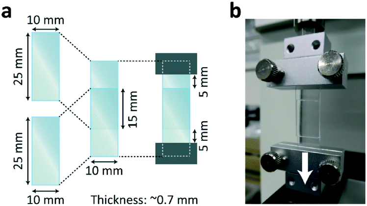 | ||
| Fig. 2 (a) Sample geometry and (b) sample setup for shear test. | ||
Comparison with modification and bonding method using plasma
The proposed method using EB and γ-rays was compared with the widely used plasma modification and bonding method. PDMS substrates were treated by low-pressure air plasma (YHS-R, Sakigake-Semiconductor Co., Ltd., 45 W) for 180 s. Subsequently, the compressive modulus, optical transparency, and WCA were measured using the same methods employed for EB- and γ-ray-irradiated samples. Chemical analysis using FT-IR and evaluation of bonding between the two PDMS substrates were also conducted. For bonding, two PDMS strips were immediately brought into contact manually after 180 s plasma treatment. Subsequently, a 100 g weight was placed over the overlapping area for 2 min.Multi-layer bonding of PDMS microfluidic devices
For multi-layer bonding, we used single-layer PDMS microfluidic devices (Microfluidic System Works Inc.) made of PDMS A with punched inlet and outlet holes. The size of the devices was 27 mm × 20 mm, and the width and depth of the channels were 200 μm and 100 μm, respectively. As a cover, a flat PDMS A substrate was prepared as described above. Six layers (five microfluidic devices with various channels and chambers and a flat cover) were stacked and then irradiated by EB for multi-layer bonding. In this experiment, a 2 MeV EB was used to increase the penetration depth. The samples were placed on a mesh stage and conveyed under a 2 mA EB shower with a dose rate of 10 J g−1 per pass. After the irradiation, blue and yellow food dyes were introduced through the inlets using syringes.Formation of 3D structures with complex shapes
The ability to form 3D structures with complex shapes, such as curved structures, Moebius loops, and coil structures using PDMS substrates, was also tested. For this, flat PDMS C substrates were cut, bent, and overlapped before undergoing EB irradiation (2 MeV, 2 mA, 10 J g−1 per pass). Some overlapping parts were tied together with PET films or paper so that the substrates would not peel apart during irradiation.Results and discussion
Enhanced rigidity
EB or γ-ray irradiation alone was apparently sufficient to cause the PDMS substrates to become rigid and lose their original deformability depending on the irradiation dose (Fig. 3a and b). This phenomenon was confirmed by changes in the compressive modulus (Fig. 3c and d): from the original value of 7 MPa, the compressive modulus of the EB-irradiated substrates became >15 MPa with a dose of 500 J g−1, and >20 MPa with a dose above 1000 J g−1. To the best of our knowledge, the stiffest PDMS A substrate in the literature has a rigidity of 10 MPa, which was achieved by adding the curing agent to the precursor at a ratio of 2:1.18 In our experiment, however, the irradiation process itself enhanced the rigidity of PDMS A, which was cured using the conventional 10:1 ratio. No major difference in compressive modulus was observed among the three types of PDMS, but for all types, EB irradiation hardened the substrates more effectively than γ-rays, with which >2500 J g−1 was required to obtain a rigidity of >20 MPa. We will discuss the mechanism for this difference later.
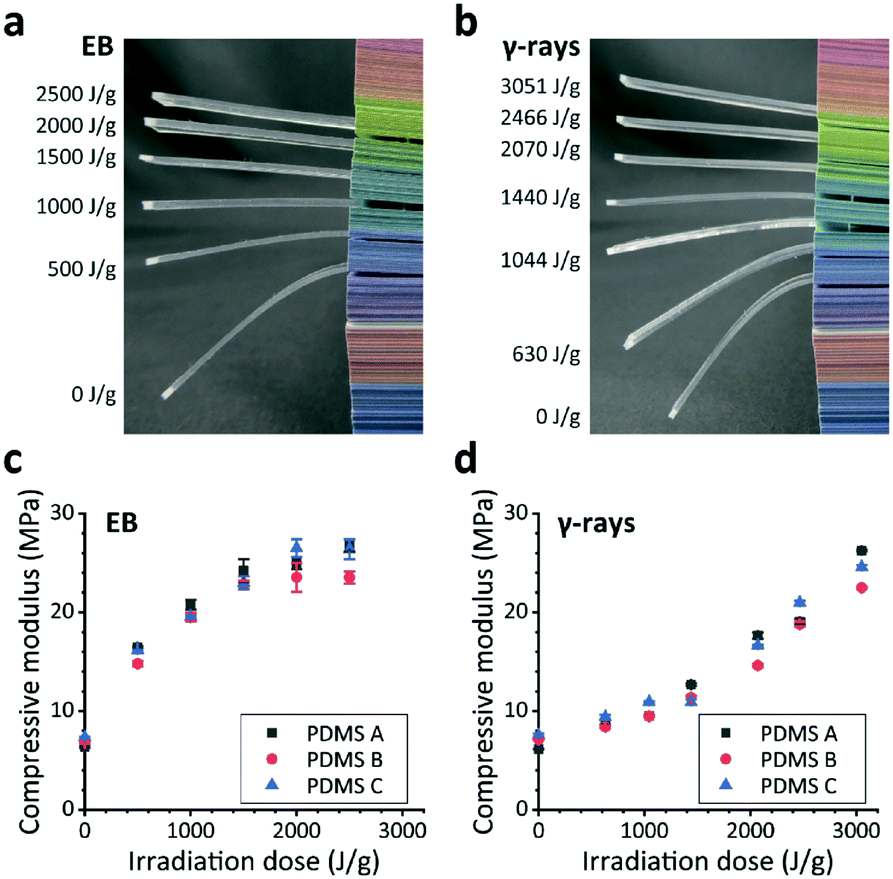 | ||
| Fig. 3 Demonstration of PDMS A substrates (5 mm wide × 35 mm long × 0.7 mm thick, put between the pages of a book) gradually losing flexibility and instead gaining rigidity in accordance with the dose of irradiation from (a) a 1 MeV electron beam (EB) and (b) 60Co γ-rays; the compressive modulus of PDMS samples as a function of the dose of irradiation from (c) a 1 MeV EB and (d) 60Co γ-rays. Error bars show the standard error of the mean for n = 3. | ||
It is known that plasma irradiation produces a rigid layer on PDMS surfaces; Mills et al. reported that oxygen-plasma irradiation resulted in a stiffness-graded layer from 37 MPa at the surface to a bulk value of 3.5 MPa at a depth of ∼200 nm by atomic force microscopy measurement.19 The thickness of this rigid layer is limited because of the plasma interaction range. In contrast, our results clearly indicate that the EB and γ-rays changed the bulk properties of the PDMS substrates by penetrating completely through them. The EB and γ-ray-irradiated substrates were free of cracking and warping, unlike those irradiated by plasma and LE-EB.11,14 Although the ranges of depth of hardening vary, it can be assumed that the mechanism for increased rigidity is similar among plasma, EB, and γ-ray irradiation, considering that the compressive modulus reported for plasma-treated PDMS surfaces19 is comparable to the obtained results (Fig. 3c and d). The details will be discussed later based on the chemical analysis investigated using FT-IR.
Optical transparency
Generally, the mechanical properties of silicones are improved by the addition of filler materials, such as silica nanoparticles20 and graphene,21 but this causes the original transparency to deteriorate. In contrast, the PDMS samples hardened by EB- or γ-ray-irradiation remained transparent. As confirmed by the UV-vis spectra (Fig. 4 and S2†), the transmittance of all three types of PDMS substrates was almost unaffected in the range of visible light (wavelength: 400–900 nm) and remained above 90%, which is suitable for microfluidic devices.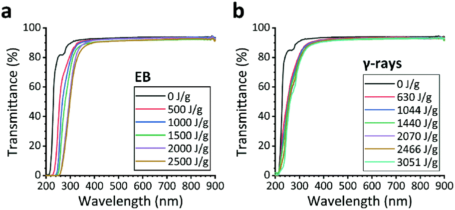 | ||
| Fig. 4 Ultraviolet-visible (UV-vis) spectra of PDMS A substrates before and after irradiation with (a) a 1 MeV electron beam (EB) and (b) 60Co γ-rays. | ||
In the wavelength range of 200–400 nm, the PDMS transmittance gradually decreased with increasing irradiation dose. This result suggests that C![[double bond, length as m-dash]](https://www.rsc.org/images/entities/char_e001.gif) C, CO, or other similar bonding may be taking place. The decrease in transmittance was greater in the EB-irradiated samples than in the γ-ray-irradiated ones, and this tendency was observed in all three PDMS types (Fig. S2†).
C, CO, or other similar bonding may be taking place. The decrease in transmittance was greater in the EB-irradiated samples than in the γ-ray-irradiated ones, and this tendency was observed in all three PDMS types (Fig. S2†).
Long-lasting hydrophilization
In addition to the hardening effect, both EB and γ-ray irradiation resulted in PDMS hydrophilization. The resultant WCAs of the PDMS substrates decreased from their original values (>110°) depending on the irradiation dose (Fig. 5a and b). It was found that EB-irradiated substrates exhibited lower WCAs than γ-ray-irradiated ones at similar irradiation doses. The results for rigidity, transmittance, and hydrophilicity all show that EB irradiation induced more dramatic chemical changes than γ-rays. There are very few reports on the hydrophilization of PDMS by ionizing radiation.14,22,23 The mechanism will be explained later with the results on chemical structural changes investigated using FT-IR.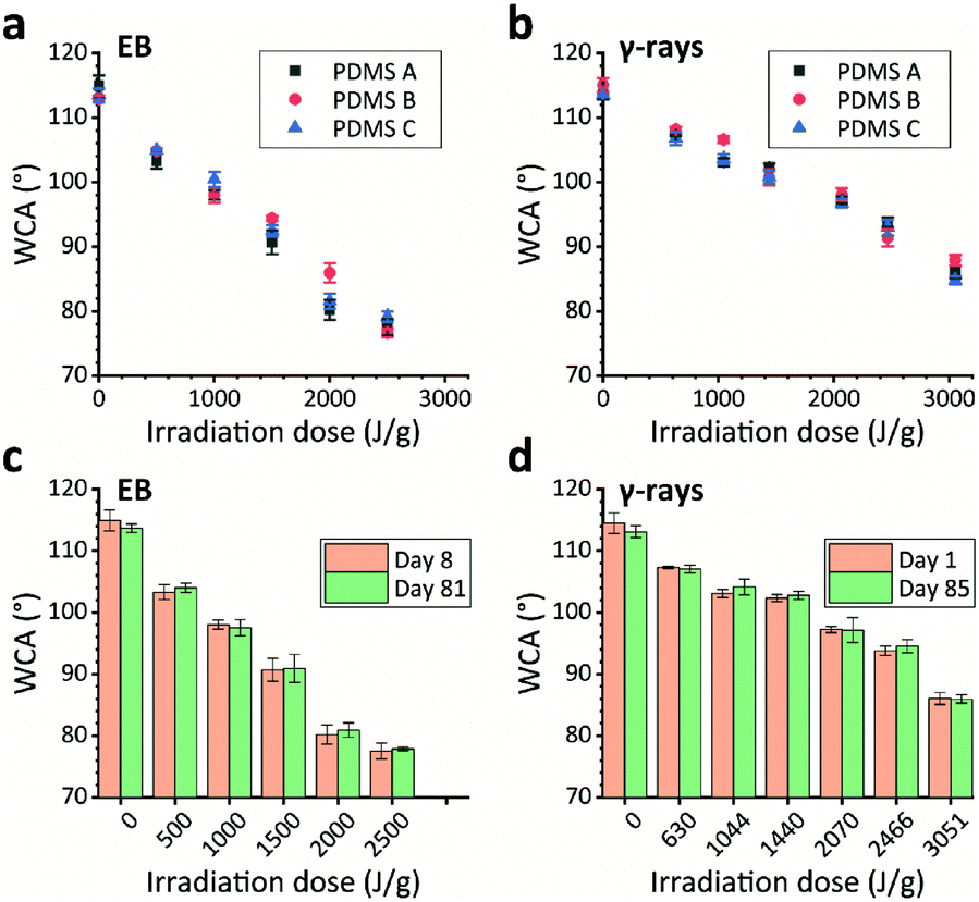 | ||
| Fig. 5 Water contact angles (WCAs) of PDMS substrates as function of irradiation dose using (a) 1 MeV electron beam (EB) and (b) 60Co γ-rays; and WCAs of PDMS A soon after irradiation by (c) EB and (d) 60Co γ-rays vs. those after storage for more than 80 days in ambient conditions. Error bars show the standard error of the mean for n = 3. | ||
Most importantly, the WCAs of EB- and γ-ray-irradiated PDMS substrates were unchanged even after storage for more than 80 days in ambient air at room temperature (∼20 °C) (Fig. 5c, d and S3†); this contrasts with hydrophilization using plasma, where the substrate recovers its hydrophobicity in mere minutes. This result supports our perspective14 that the thickness of the hydrophilized layer is a key factor in prolonging hydrophilicity because it can hinder the reorientation of nonpolar groups from the bulk to the surface. Both the 1 MeV EB and the γ-rays completely penetrate the PDMS substrates and change the bulk into hydrophilic materials; thus, the hydrophobicity cannot be recovered. No major difference was observed among the three PDMS types regarding hydrophilicity and its durability.
Absorption/adsorption of hydrophobic small molecules
Using rhodamine B as a model drug,17 the absorption/adsorption of small molecules in the PDMS substrates was evaluated. After storage for >80 days in ambient air at room temperature (∼20 °C), non-irradiated and EB- and γ-ray-irradiated PDMS substrates were soaked in 1 μM rhodamine B solution for 60 min. The red coloration in the cross-section fluorescence images of the substrates represents the distribution of rhodamine B (Fig. 6a); the dye attached to the surface is seen as a deep red horizontal line. The samples were then soaked in ultrapure water for 10 min. The fluorescence intensity of a representative image for each sample was plotted against the depth from the sample surface (Fig. 6b and c). The intensity values were normalized using the maximum value for a non-irradiated sample soaked in the dye for 60 min. | ||
| Fig. 6 Absorption/adsorption of rhodamine B in non-irradiated and 1 MeV electron beam (EB)-irradiated PDMS A substrates evaluated after storage for 83 days in ambient conditions. The cross-section images of the substrates (a) were obtained by confocal fluorescence microscopy; the triangle beside each picture indicates the position of the substrate surface. The distribution of rhodamine B was evaluated in terms of the image intensity after (b) soaking in rhodamine B for 60 min and (c) subsequent soaking in ultrapure water for 10 min. | ||
Although glare from bright surfaces increased the background intensity above and below the focal plane (because we avoided image restoration by deconvolution), it is clear that the non-irradiated PDMS A absorbed rhodamine B inside the substrate. Soaking in water for 10 min could not remove rhodamine B from the non-irradiated sample; in contrast, this soaking process resulted in the diffusion of the dye inside the substrates. However, both absorption and adsorption of rhodamine B were markedly suppressed after irradiation. The dye hardly adhered to the surface of the sample that was EB-irradiated at 2500 J g−1. A small amount of dye on the surface of the sample that was EB-irradiated at 2000 J g−1 was removed by simple immersion in ultrapure water for 10 min without shaking.
As expected from the different effects of EB and γ-ray irradiation on PDMS rigidity and hydrophilicity as described above, the suppression of absorption/adsorption properties of PDMS was more effective with irradiation by EB than by γ-rays (Fig. S4†). Similar results were obtained for PDMS B and C. The hydrophilization and the structural changes in bulk (demonstrated by the enhanced rigidity) of the irradiated PDMS considerably reduced the absorption/adsorption of hydrophobic small molecules even after more than 80 days had passed since the irradiation.
Various modification methods have been proposed to degrade the absorption/adsorption properties of PDMS, such as plasma irradiation,24 grafting,25 or mixing with functional polymers.26,27 In contrast with these methods, the method proposed here requires no additives or reagents and enables long-lasting modification with high throughput.
Chemical changes in PDMS
The results above show that both EB and γ-ray irradiation changed PDMS into a rigid, stably hydrophilized, and low-absorption/adsorption material while maintaining the transparency of the substrate in the visible-light region. The chemical changes induced were analyzed using FT-IR spectroscopy (Fig. 7 and S5†). In the full spectra of the non-irradiated and irradiated PDMS substrates, only small differences are apparent; in the expanded spectra, however, an increase in the peak around 1010 cm−1 (Si–O–Si bonds) and a decrease in the peak around 790 cm−1 (–CH3 bonds) can be seen with increasing irradiation dose. Note that the peak intensity may be influenced by the sample rigidity. The intensities for rigid samples, which require more pressure for good contact with the ATR crystal than soft samples, might be underestimated because the same pressure was applied for all samples. Although quantitative analysis is difficult, the results showing the decrease in –CH3 bonds and increase in Si–O–Si bonds are consistent with the findings of our previous study analyzing LE-EB irradiation effects on PDMS surfaces using X-ray photoelectron spectroscopy.14 The three PDMS types have similar FT-IR spectra, and the spectral changes are greater with irradiation by EB than by γ-rays (Fig. S5†). | ||
| Fig. 7 Fourier transform infrared (FT-IR) spectra of non-irradiated and 1 MeV electron beam (EB)-irradiated PDMS A: (a) full spectrum and (b–d) expanded spectra. | ||
Although their energy absorption processes are different, EBs and γ-rays both generate secondary electrons in polymers through ionization and induce essentially the same subsequent chemical reactions.15 There are several reports on radiation-induced chemical reactions in PDMS. Hill et al. showed that crosslinking is more likely to occur than chain scission in PDMS upon γ-ray irradiation, and identified the crosslinking structures using nuclear magnetic resonance.28,29 Their results also indicated the decrease in –CH3 bonds and the formation of Si–O–Si bonds. Like plasma, EB and γ-rays decompose –CH3 side groups, which evaporate from the matrix as gases such as H2 and CH4.30 Some of the decomposed –CH3 groups change into CC and CO, as suggested by the decrease in transmittance in the 200–400 nm wavelength region (Fig. 4 and S2†). PDMS also reacts with ambient oxygen and will form hydrophilic Si–OH (silanol) groups instead of hydrophobic –CH3. Both the silanol groups and Si· and O· produced by main-chain scission trigger the formation of Si–O–Si bridges and convert PDMS into a Si–Ox-rich (where x is 3 or 4) crosslinked structure. Owing to its high dose rate, which was ∼500 times higher than that of the γ-rays, EB irradiation induced chemical changes and modified the PDMS more efficiently than the γ-rays. Heat produced by high-dose-rate EB irradiation can also promote crosslinking reactions in PDMS.28 Although we minimized the heat by placing the samples on a cooled stage, some heat may have accumulated inside the samples.
Although the chemical reactions induced are similar, there is a major difference between plasma and EBs/γ-rays in their ranges of interaction in PDMS. EBs and γ-rays penetrate and modify PDMS in the range of millimeters (Fig. S1†) to meters.15 We believe, on the basis of our results, that intrinsic gas permeability allows crosslinking deep inside the bulk through evaporation of decomposed –CH3 and intake of ambient oxygen, as described above. The fully crosslinked PDMS substrates acquired favorable characteristics that are completely different from those of the original PDMS such as enhanced rigidity, long-lasting hydrophilicity, and remarkably suppressed absorption/adsorption properties.
Bonding between PDMS substrates
We found that EB and γ-rays not only modify the PDMS bulk but also bond stacked PDMS substrates. For detailed evaluation, shear testing was performed on two-layer stacked PDMS substrates. The samples, composed of two overlapping PDMS strips (overlapped area: 10 mm wide × 15 mm long, Fig. 2a), were pulled by moving one of the grips clamping the ends (Fig. 2b). The non-irradiated samples only adhered to each other physically; thus, they were easily separated into the two intact original substrates by pulling. By contrast, all of the EB- or γ-ray-irradiated samples were fractured by pulling. This type of failure occurs when the strength of the bond is equal to or greater than that of the material bonded. Thus, it was clearly shown that the PDMS substrates were chemically bonded by crosslinking between their interfaces by irradiation even at the relatively low dose of 500 J g−1 for EB irradiation and 630 J g−1 for γ-rays.As shown by the shear load–extension curves (Fig. 8 and S6†), the maximum load values that mark the onset of separation or failure increased markedly after EB or γ-ray irradiation. It is difficult to assess bond strength from these results because the substrates as a whole were changed mechanically by irradiation. The samples irradiated with doses of 500 J g−1 and 1000 J g−1 somewhat preserved their original flexibility (Fig. 3a) and extended for ∼4.5 mm and ∼3 mm, respectively. However, the decrease in extension with increasing irradiation dose indicates that samples lost their original elasticity as rubber and became brittle instead. The PDMS substrates bonded by EB irradiation showed higher maximum load values than those bonded by γ-rays (Fig. S6†). Among the three types of PDMS, PDMS C exhibited the highest load value and the greatest extension at the breaking point. The high bond strength and retention of flexibility of PDMS C may be attributable to its high purity.
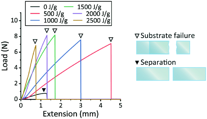 | ||
| Fig. 8 Shear load–extension curves obtained for non-irradiated and 1 MeV electron beam (EB)-irradiated PDMS A. The triangles indicate whether the tests ended with separation of the intact substrates (black triangle) or substrate failure (white triangles). | ||
The interfaces of stacked materials are rarely chemically bonded solely by irradiation using ionizing radiation. We believe that the crosslinking between PDMS interfaces is promoted by the high mobility of molecular chains due to the low Tg. Nishi et al. reported that adhesion forces between PDMS and other polymers such as polypropylene (PP),31 polytetrafluoroethylene (PTFE),32 and polymethyl methacrylate (PMMA)33 became stronger when two films were compressed and irradiated by low-energy EBs (0.17 MeV). The mobilities of the molecular chains of these polymers are low at room temperature because of the high Tg, but all of these polymers have low radiation resistance. The radicals produced via main-chain scission of these polymers might interact with PDMS molecules by pressing against each other. Our PDMS–PDMS bonding, in contrast, did not require compression during the irradiation owing to the high mobility of the molecules on both sides. As the result, micropatterns on the bonded interfaces can be prevented from being deformed due to compression. It should be noted that the PDMS samples did not bond to the PET-based radiation–sterilization bags nor the PET films we used. We believe that the high radiation resistance of PET prevents it from reacting with PDMS.
Comparison with modification and bonding method using plasma
We compared the proposed method using EB and γ-rays with a widely used modification and bonding method using plasma. Unlike EB and γ-rays (Fig. 3), plasma irradiation did not affect the mechanical properties of the bulk substrate (Fig. S7a†) because plasma produces a rigid layer only at the surface.19 The plasma-irradiated PDMS substrates remained transparent as shown in the UV-vis spectra (Fig. S7b†). Although EB- and γ-ray-irradiated substrates also remained transparent (Fig. 4), the spectral changes observed for the plasma-irradiated samples were much smaller than those for EB- and γ-ray-irradiated ones. This is also due to the different penetration ranges, which affect where chemical reactions are induced. The plasma-modified layer was too thin to be detected by FT-IR spectroscopy (Fig. S7c†). The plasma effectively modified only the surface of PDMS substrates: the WCA evaluated within 1 h after the plasma-irradiation was ∼33° (Fig. S7d†). This value is lower than those obtained by EB- or γ-ray-irradiation (Fig. 5); however, the plasma-irradiated surface soon recovered its original hydrophobicity during storage in ambient air at room temperature (∼20 °C) (Fig. S7d†). Due to this instability, substrate bonding by plasma requires immediate contact of the PDMS surfaces after irradiation. In contrast, EB and γ-rays irreversibly bond PDMS surfaces during irradiation. Moreover, a difference between the two bonding methods was observed in the shear load–extension curves (Fig. S7e†). Plasma irradiation bonded the substrates while preserving the original elasticity of PDMS; thus, longer extension and higher maximum load values were obtained compared to EB-/γ-ray-irradiation, which mechanically changed the bonded substrates as a whole (Fig. 8 and S6†). As revealed by these comparison results, essentially, the main difference between plasma and EB-/γ-rays is the interaction range in PDMS: plasma modifies only the surface, but EB and γ-rays modify the bulk and can modify many stacked substrates, depending on the irradiation dose.Production of 3D integrated microfluidic chips
Both EBs and γ-rays irreversibly bonded PDMS substrates in addition to simultaneously inducing various modifications. Using these salient effects, we produced 3D integrated microfluidic chips (Fig. 9). For this, six PDMS layers (five microfluidic devices and a flat cover) were stacked and then irradiated by a 2 MeV EB. By the flow of blue and yellow food dyes introduced through the inlets, it was verified that our method enabled leak-proof multi-layer bonding between the six layers. The blue and yellow solutions flowed separately from the first to the fourth layer via the various microchannels and chambers and then mixed in the fifth layer. The mixed solution (green) flowed from the fifth layer to the outlet in the first layer as designed. The multi-layer-bonded chip functioned successfully as a 3D integrated chip.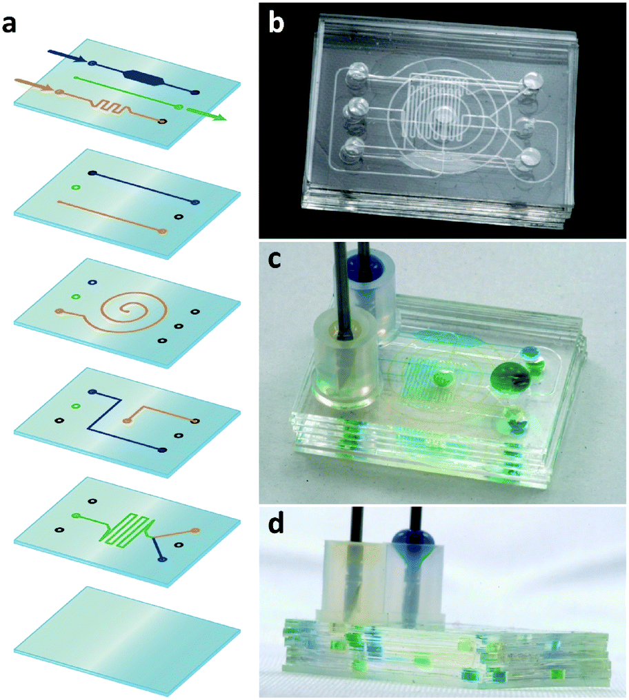 | ||
| Fig. 9 3D integrated microfluidic chip produced by 2 MeV electron beam (EB) irradiation. (a) Six stacked layers (five microfluidic devices and a cover) made of PDMS A were (b) irreversibly bonded by EB irradiation, and (c and d) blue and yellow dyes flowed through them three-dimensionally as planned. | ||
As clearly demonstrated by successful multi-layer bonding, the EB/γ-rays penetrated through the stacked layers and induced chemical changes in all layers. That is, EB/γ-rays can chemically bond the contact interfaces between layers and simultaneously modify all the layers including the internal microchannels and chambers. Therefore, the proposed EB-/γ-ray-irradiation method can produce rigid, transparent, hydrophilized, and low-absorption/adsorption 3D integrated microfluidic chips. The bonding of multiple layers is achieved with high-throughput yield because the layers bond after re-adjustable alignment. Furthermore, this method can be applied to stacked PDMS substrates sealed in their final packages; thus, the chips obtained were radiation-sterilized simultaneously with modification and bonding. Moreover, unlike the one-at-a-time process using plasma, mass production of 3D chips is possible using commercial radiation sterilization facilities. Data from 2019 reveal that more than 200 γ-ray and thousands of EB facilities are operating in 55 countries to sterilize medical and healthcare products including gloves, syringe needles, and cell culture dishes.34 The processing time can be significantly reduced when high-dose-rate EB is adopted: full irradiation with a dose of 25 J g−1 (the general sterilization dose) is completed within seconds;35 hence, the proposed method can be conducted within several minutes. Bonding takes several days if γ-rays are selected; however, large-quantity processing is still possible owing to the high penetration range.15,34 Usually, the cost of the irradiation is calculated per box (space) and per irradiation dose. Many stacked PDMS substrates can be irradiated after they are separately sealed in sterilization bags to prevent bonding between the 3D chips, and to keep them sterile after irradiation. The cost of EB-irradiation per box (340 × 400 × 400 mm3) at a dose of 25 J g−1 was approximately 2000–2500 JPY (approximately 18–23 USD) in Japan as of 2004.36 Given the density of PDMS (∼0.97 g cm−3), the height of the box is limited to ∼100 mm when 10 MeV-EB is used (Fig. S1†). If the irradiation box (340 × 400 × 100 mm3) is filled with 800 chips in sterilization bags (estimated size: 30 × 50 × 10 mm3) and the box is irradiated with EB at 1000 J g−1, the estimated cost will be 1 USD per chip or less. Based on information from the website of one commercial EB provider,35 the recent cost for radiation sterilization is expressed in “dollars per cubic foot”. If the irradiation cost for 25 J g−1 is 10 USD, and if the box (300 × 300 × 100 mm3) is filled with 600 chips and irradiated at 1000 J g−1, the cost will be 0.7 USD per chip or less. However, it should be noted that the cost per chip depends on the number of chips contained in one irradiation box. If only a small number of chips are fabricated and placed in the box, for example 10 chips, the cost will be 42 USD per chip. The proposed method will be cost-effective when large quantities are involved. Nevertheless, such mass-production capability and ready-to-use practicality of the proposed method have never before been achieved in 3D chip production. We believe our method will bridge the gap between academia and industry by enabling the low-cost mass production of 3D chips whose concept and effectiveness have been examined by using the easily accessible plasma bonding technique.
Formation of 3D structures with complex shapes
In addition to the production of modified single-layer or multi-layer PDMS microfluidic chips, the proposed method can be used to obtain a variety of 3D structures with complex shapes. As we demonstrated, EBs and γ-rays can harden and bond flexible PDMS materials. Therefore, by cutting, performing origami-style folding, and making contact between components before irradiation (Fig. S8a†), complex structures can be produced that are difficult to fabricate by conventional methods such as cut processing and injection molding (Fig. 10 and S8b†). Although 3D printers have emerged as a potential next-generation technology for the fabrication of 3D devices, including microfluidic ones, there are still major issues concerning patterning resolution and throughput.37 The combined use of precise and repeatable micro/nanopatterning of PDMS by conventional soft lithography and hardening/bonding by the proposed method offers a novel approach for obtaining specialized 3D structures that are currently in demand in a variety of fields including electronics, photonics, energy, and biomedicine.38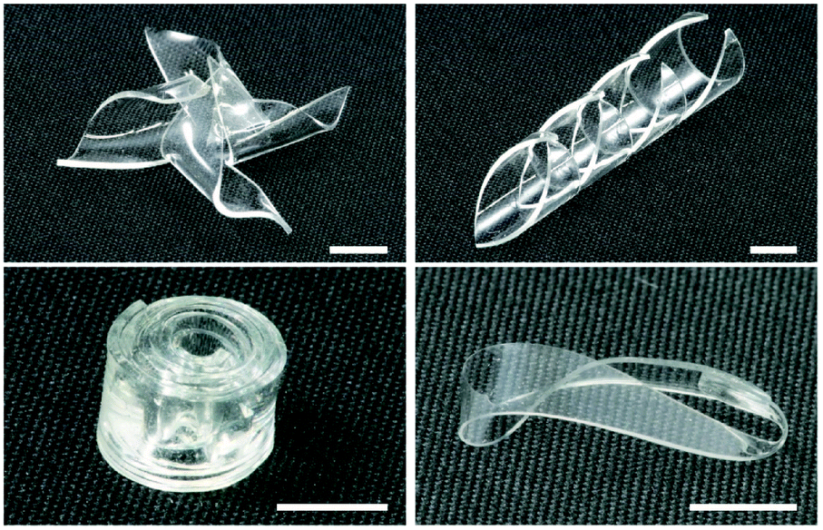 | ||
| Fig. 10 Cut, folded, and overlapped PDMS C films were integrated into structures with complex 3D shapes by the hardening and bonding effects induced by 2 MeV electron beam irradiation. Scale bars are 5 mm. | ||
Conclusions
In this paper, we have introduced a simple and high-throughput method for obtaining hydrophilic, rigid, low-absorption/adsorption, and sterilized multi-layer 3D integrated PDMS microfluidic chips by utilizing chemical reactions induced by EB and 60Co γ-rays. The proposed method can also be used for producing 3D structures with complex shapes that are difficult to fabricate with plastic or glass. PDMS's advantages, such as the ease of molding in soft lithography, biocompatibility, and optical transparency, are not impaired because no chemical crosslinkers, adhesive agents, or fillers are required in this method. Importantly, mass production of 3D chips and 3D structures is possible at low cost using commercial radiation–sterilization facilities.Both EB and γ-rays can be used for this new PDMS bonding method. As revealed in this study, EB can modify PDMS more efficiently than γ-rays owing to its high dose rate. However, the depth-dependent dose difference should be carefully considered especially when EB is applied. The 3D chips should be irradiated from both sides similar to the current radiation sterilization process. For the mass production of reliable 3D chips, the dose uniformity within an irradiation box should be precisely assessed for both EB and γ-rays. The irradiation dose should be selected according to the purpose; for example, 500 J g−1 will be sufficient for bonding, but more than 1000 J g−1 will be required to avoid nonspecific adsorption and absorption. For applications which require flexibility, such as wearable devices, nonspecific adsorption and adsorption may be insufficiently minimized because the irradiation dose required will be lower. Although we found no significant differences among the three PDMS types having different amounts of low-MW siloxane except in bonding strength, material optimization in future work may enable more effective modification and bonding at lower irradiation doses. Further, several other additional processes will be required for guaranteeing the desired chemical and mechanical properties of the internal microchannels and chambers of the 3D chips, such as hydrophilicity, absorption/adsorption level, and rigidity. The evaluation of the actual bonding strength between multilayers and the influence of hydrophilization and enhanced rigidity on microchannel flow should be also studied. For the mass production of 3D microfluidic chips, additional considerations will be needed, such as the precise and automated alignment and stacking of the layers using robot hands, and the packing style to keep the stacked substrates flat and to prevent unnecessary compression.
The favorable properties of 3D integrated microfluidic chips produced using the new method as summarized above, especially low-cost mass-production capability and ready-to-use practicality, can bridge the gap between academia and industry and facilitate the application of PDMS-based chips to a variety of fields, particularly diagnostics and pharmaceuticals. In addition, the production of 3D structures with complex shapes using the proposed method will open up new possibilities for 3D devices in a wide variety of applications including microfluidics.
Author contributions
T. G. O. conceived and initiated the project. T. G. O., K. O., and M. T. designed, and T. G. O. performed, experiments. T. G. O. and K. O. analyzed the data, and T. G. O., K. O., and M. T. wrote the manuscript.Conflicts of interest
T. G. O. and M. T. are co-inventors for a patent related to this study.Acknowledgements
The authors thank Dr. Yuji Hosaka (QST) for helping with the simulation of the EB penetration depth; Ms. Ryoko Mezaki (QST) for helping with sample preparation, especially in the fabrication of the 3D structures with complex shapes; Ms. Noriko Tawara (QST) for technical assistance with irradiation and measurements; and Mr. Ichiro Takahashi (QST) for taking the sample photographs shown in Fig. 9, 10, and S8.† T. G. O. was supported by a Japan Society for the Promotion of Science KAKENHI Grant (JP18K18390) and the QST President's Strategic Grant (Creative Research).References
- J. C. McDonald, D. C. Duffy, J. A. Anderson, D. T. Chiu, H. Wu, O. J. A. Schueller and G. M. Whitesides, Electrophoresis, 2000, 21, 27–40 CrossRef CAS.
- M. W. Toepke and D. J. Beebe, Lab Chip, 2006, 6, 1484–1486 RSC.
- B. S. Hardy, K. Uechi, J. Zhen and H. P. Kavehpour, Lab Chip, 2009, 9, 935–938 RSC.
- C. Kang, C. Roh and R. A. Overfelt, RSC Adv., 2014, 4, 3102–3112 RSC.
- Y. Temiz, R. D. Lovchik, G. V. Kaigala and E. Delamarche, Microelectron. Eng., 2015, 132, 156–175 CrossRef CAS.
- D. C. Duffy, J. C. McDonald, O. J. A. Schueller and G. M. Whitesides, Anal. Chem., 1998, 70, 4974–4984 CrossRef CAS PubMed.
- M. A. Unger, H. P. Chou, T. Thorsen, A. Scherer and S. R. Quake, Science, 2000, 288, 113–116 CrossRef CAS PubMed.
- M. A. Eddings, M. A. Johnson and B. K. Gale, J. Micromech. Microeng., 2008, 18, 067001 CrossRef.
- M. Zhang, J. Wu, L. Wang, K. Xiao and W. Wen, Lab Chip, 2010, 10, 1199–1203 RSC.
- M. Chu, T. T. Nguyen, E. K. Lee, J. L. Morival and M. Khine, Lab Chip, 2017, 17, 267–273 RSC.
- S. Béfahy, P. Lipnik, T. Pardoen, C. Nascimento, B. Patris, P. Bertrand and S. Yunus, Langmuir, 2010, 26, 3372–3375 CrossRef PubMed.
- J. Zhou, A. V. Ellis and N. H. Voelcker, Electrophoresis, 2010, 31, 2–16 CrossRef CAS PubMed.
- M. Li and D. P. Kim, Lab Chip, 2011, 11, 1126–1131 RSC.
- T. G. Oyama, B. J. D. Barba, Y. Hosaka and M. Taguchi, Appl. Phys. Lett., 2018, 112, 213704 CrossRef.
- Q. Q. Qiu, W. Q. Sun and J. Connor, Comprehensive Biomaterials, Volume 4: Biocompatibility, Surface engineering, and Delivery of Drugs, Genes and Other Molecules, ed. P. Duchevne, Elsevier, Amsterdam, 1st edn, 2011, pp. 127–144 Search PubMed.
- W. S. Rasband, ImageJ, U. S. National Institutes of Health, Bethesda, Maryland, USA, 1997–2018, Available from: https://imagej.nih.gov/ij Search PubMed.
- M. A. Iyer and D. T. Eddington, Lab Chip, 2019, 19, 574–579 RSC.
- R. Seghir and S. Arscott, Sens. Actuators, A, 2015, 230, 33–39 CrossRef CAS.
- K. L. Mills, X. Zhu, S. Takayama and M. D. Thouless, J. Mater. Res., 2008, 23, 37–48 CrossRef CAS PubMed.
- J. Liu, G. Zong, L. He, Y. Zhang, C. Liu and L. Wang, Micromachines, 2015, 6, 855–864 CrossRef.
- K. Zeranska-Chudek, A. Lapinska, A. Wroblewska, J. Judek, A. Duzynska, M. Pawlowski, A. M. Witowski and M. Zdrojek, Sci. Rep., 2018, 8, 9132 CrossRef CAS PubMed.
- D. W. Kang, I. S. Kuk, C. H. Jung, I. T. Hwang, J. H. Choi, Y. C. Nho, S. Mun and Y. M. Lee, Polymer, 2011, 35, 157–160 CAS.
- R. Huszank, D. Szikra, A. Simon, S. Z. Szilasi and I. P. Nagy, Langmuir, 2011, 27, 3842–3848 CrossRef CAS PubMed.
- L. J. Waters, C. V. Finch, A. K. M. M. H. Bhuiyan, K. Hemming and J. C. Mitchell, J. Pharm. Anal., 2017, 7, 338–342 CrossRef PubMed.
- Z. Zhang, X. Feng, Q. Luo and B. F. Liu, Electrophoresis, 2009, 30, 3174–3180 CrossRef CAS PubMed.
- J. Zhou, H. Yan, K. Ren, W. Dai and H. Wu, Anal. Chem., 2009, 81, 6627–6632 CrossRef CAS PubMed.
- A. Gökaltun, Y. B. A. Kang, M. L. Yarmush, O. B. Usta and A. Asatekin, Sci. Rep., 2019, 9, 7377 CrossRef PubMed.
- D. J. T. Hill, C. M. L. Preston, D. J. Salisbury and A. K. Whittaker, Radiat. Phys. Chem., 2001, 62, 11–17 CrossRef CAS.
- D. J. T. Hill, C. M. L. Preston and A. K. Whittaker, Polymer, 2002, 43, 1051–1059 CrossRef CAS.
- A. A. Miller, J. Am. Chem. Soc., 1960, 82, 3519–3523 CrossRef CAS.
- Y. Nishi, H. Kawazu, H. Takei, K. Iwata, H. Kudoh and K. Mitsubayashi, Mater. Trans., 2011, 52, 1943–1948 CrossRef CAS.
- Y. Nishi, M. Uyama, H. Kawazu, H. Takei, K. Iwata, H. Kudoh and K. Mitsubayashi, Mater. Trans., 2012, 53, 1657–1664 CrossRef CAS.
- R. Yamaguchi, A. Yagi, C. Kubo, M. Kanda and Y. Nishi, J. Jpn. Inst. Met. Mater., 2016, 80, 503–507 CrossRef CAS , (in Japanese).
- I. Obodovskiy, Radiation: Fundamentals, Applications, Risks, and Safety, Elsevier, The Netherlands, 2019 Search PubMed.
- E-BEAM Services, Inc. How does the electron beam sterilization process work? [Internet]. (Accessed March 2020). Available from: https://ebeamservices.com/blog/how-does-the-electron-beam-sterilization-process-work/.
- M. Tabei, H. Kudo and Y. Katsumura, Radioisotopes, 2004, 53, 483–490 CrossRef , (in Japanese).
- N. P. Macdonald, J. M. Cabot, P. Smejkal, R. M. Guijt, B. Paull and M. C. Breadmore, Anal. Chem., 2017, 89, 3858–3866 CrossRef CAS PubMed.
- Y. Zhang, F. Zhang, Z. Yan, Q. Ma, X. Li, Y. Huang and J. A. Rogers, Nat. Rev. Mater., 2017, 2, 17019 CrossRef CAS.
Footnote |
| † Electronic supplementary information (ESI) available: Fig. S1–S8. See DOI: 10.1039/d0lc00316f |
| This journal is © The Royal Society of Chemistry 2020 |