
Contactless sensing of liquid marbles for detection, characterisation & computing†
Thomas C.
Draper‡
 a,
Neil
Phillips
a,
Roshan
Weerasekera
ab,
Richard
Mayne
ac,
Claire
Fullarton
a,
Ben P. J.
de Lacy Costello
ad and
Andrew
Adamatzky
a
a,
Neil
Phillips
a,
Roshan
Weerasekera
ab,
Richard
Mayne
ac,
Claire
Fullarton
a,
Ben P. J.
de Lacy Costello
ad and
Andrew
Adamatzky
a
aUnconventional Computing Laboratory, University of the West of England, Bristol, BS161QY, UK. E-mail: Tom.Draper@uwe.ac.uk
bDepartment of Engineering Design and Mathematics, Faculty of the Environment and Technology, University of the West of England, Bristol, BS161QY, UK
cDepartment of Applied Sciences, Faculty of Health and Applied Sciences, University of the West of England, Bristol, BS161QY, UK
dInstitute of Biosensing Technology, Centre for Research in Biosciences, University of the West of England, Bristol, BS161QY, UK
First published on 21st November 2019
Abstract
Liquid marbles (LMs) are of growing interest in many fields, including microfluidics, microreactors, sensors, and signal carriers. The generation of LMs is generally performed manually, although there has recently been a burst of publications involving ‘automatic marble makers’. The characteristics of a LM is dependent on many things, including how it is generated, it is therefore important to be able to characterise LMs once made. Here is presented a novel contactless LM sensor, constructed on a PCB board with a comb-like structure of 36 interlacing electrical traces, 100 μm wide and 100 μm apart. This cheap, scalable, and easy to use sensor exploits the inherent impedance (comprised of the electrical resistance, capacitive reactance and inductive reactance) of different LMs. With it, parameters of a LM can be easily determined, without interfering with the LM. These parameters are (1) particle size of the LM coating, (2) the concentration of a NaCl solution used as the LM core, and (3) the volume of the LM. Additionally, due to the comb-like nature of the sensor, the accurate positioning (down to the inter-trace spacing) of the LM can be ascertained. The new sensor has been shown to work under both static and dynamic (mobile) conditions. The capacitance of a LM was recorded to be 0.10 pF, which compares well with the calculated value of 0.12 pF.
1 Introduction
A single, sessile droplet of water on a solid smooth surface, typically wets said surface. This is a result of the reduction of the droplet's surface energy. The extent of the wetting is determined by the energy of the solid substrate, which is qualitatively termed its hydrophobicity; the more hydrophobic, the less the droplet wets the surface. There are two primary routes for decreasing the wetting of a surface: modify the surface, or modify the droplet.Liquid marbles (LMs) are an increasingly popular1–5 modification to the droplet. Initially reported by Aussillous and Quéré in 2001,6 they are comprised of a droplet of liquid, surrounded by hydrophobic particles adhered to the surface of the droplet. By having such an ‘armoured droplet’, the effects of wetting are nullified. A LM can freely move around on a typically wetting surface, with minimal hindrance or hysteresis, and no loss of volume due to adhesion. This provides many advantages to microfluidics,7 and creates a great many other applications for LMs. These include rapid blood-typing assays,8 unconventional computation signals,9 and control of micro-encapsulated reactions.10,11
LMs provide additional advantages in microfluidics. Due to the powder coating on the surface of the droplet, the evaporation rate of the liquid core can be reduced,12–15 providing ease and flexibility to experimental setups. Resultantly the oil phase, traditionally present in microfluidic systems, can also be removed as it is no longer required for heat dissipation during reactions. This helps to remove any cross-contamination that may have occurred through the oil phase, as well as reducing the energy required for heating.
The development of microfluidics has enabled massive reductions in the quantity of both reagents and waste, helping to reduce costs and keep chemistry greener. Movement of droplets through digital microfluidic devices16 is normally achieved through electrowetting on dielectric (EWOD),17 surface acoustic waves (SAW),18 or thermocapillary actuation.19 Once the droplet has been relocated, sensing the new position of the droplet is required. Capacitance measurement provides for a means of achieving this in a non-invasive manner20–23 (though other techniques, such as labelling,24 are also used).
Microfluidic systems using LMs can also use EWOD for actuation,25,26 though due to the low hysteresis and lack of wetting the marbles can also roll under gravity.27 The coalescence of two LMs can be controlled through many techniques, such as collisions,28–30 acoustic waves,31 or electrical potential.32–34 This enables the controlled initiation of reactions. Continued efforts to enable complete automation of such devices necessitates the ability to accurately determine the positions of LMs.
We report on the first use of impedance and capacitance to accurately and reliably determine the presence and properties of a LM. Using a custom-made printed circuit board (PCB) and a high frequency AC supply, the voltage drop across an in-series shunt resister provides the necessary information. The purpose of the device is to detect the location of a LM, whilst simultaneously providing quantifiable information on some of the LM's properties. Such detection is increasingly required as the complexity of the paths and/or interactions between LMs increase. Whilst it is sometimes possible to use high-speed cameras for this purpose, optical tracking can be very expensive and doesn't scale easily, as the LM paths can become increasingly obscured in large 3D structures. We propose that this system will be useful in a range of fields, from digital microfluidics (e.g. for the real-time monitoring of LM location and properties) to unconventional computing (e.g. for determining if a billiard ball-style collision has resulted in a coalesced LM of a larger volume).
2 Experimental
LMs were made by rolling a droplet of either deionised water (DIW) or an aqueous NaCl solution on an appropriate hydrophobic powder bed. Droplets were dispensed using an air-displacement micropipette. The powders used were ultra-high density polyethylene (PE) (Sigma-Aldrich, 3–6 × 10⁶ g mol−1) or polytetrafluoroethylene (PTFE) (Alfa Aesar, 6–10 μm). The PE powder was sieved using a micro-sieve set (Sigma-Aldrich, Z675415) in order to provide powders with a variety of particle sizes: 63 μm to 90 μm, 90 μm to 125 μm, 125 μm to 180 μm, and 180 μm to 250 μm. The NaCl solutions (5 wt%, 10 wt%, 15 wt%, 20 wt%, 25 wt%, and saturated) were made either by saturation of DIW (15 MΩ cm) at 21 °C with NaCl (Fisher Scientific), or by solvation of an appropriate amount of NaCl in DIW. All reagents were used as received. The newly formed LMs were rolled by hand on the powder bed for approximately 10 s to ensure a good and complete coating.The main experimental system was designed such that it would be small, cheap and scalable. The sensor itself is an array of two sets of 18 traces (small copper tracks) on a PCB, shown in Fig. 1(a), with each set of 18 traces connected to each other to maximise sensitivity. A range of geometries and forms were considered for the electrode arrays. The area of direct contact between the marble's powder coating and surface of electrode array depends on several factors in particular the volume of the marble. For 20 μl volume the area of direct contact is approximately 3.5 mm2, therefore the resolution of the electrode array needed to be fine, as the influence of changing relative permittivity varies with the inverse square of distance. Consequently the electrode conductors, and gaps between them, were made as narrow as practical. Using ‘standard’ PCB manufacturing facilities provided 100 μm traces with 100 μm gaps (on a two layer board). Alternative methods of forming the conductors (such as printing conductive inks) were investigated but they didn't offer substantial benefits over PCBs. To minimise electrical noise (from external sources) a ground plane was located on the bottom layer of the PCB (which connected to ground on instrumentation) and the fibreglass (FR4) middle portion of the board was made as thin as practical (0.4 mm). The width of the traces from the electrode array were tapered to reduce electrical resistance and tight bends were avoided to reduce impedance at higher frequencies.
 | ||
| Fig. 1 (a) The diagram of the PCB sensor. (b) A cartoon design of the PCB sensor within the holder, with the (simplified) electrical traces visible as yellow tracks. (c) A side photograph of a 30 μL PTFE LM, with dimensions 4.0 mm wide and 2.9 mm high. The scale bar is 2.0 mm. | ||
The thinness of the board (0.4 mm) meant that it had a degree of flexibility. We exploited this by curving the PCB, so that the sensor grid was at the bottom and the electrical connectors were at the top (i.e. the electrical traces ran down either side of the slope). This shape was maintained through use of a custom made 3D-printed support, visible in Fig. 1(b). The new curvature of the PCB means that the LM is always centred to the sensor, along one axis.
The small insulated gaps between the traces mean that there is a large resistance across the circuit under DC, however under AC the system acts like a capacitor. This can be easily confirmed by application of a square wave to the system and monitoring via an oscilloscope, resulting in the characteristic curved profile.
The sensing grid was positioned in series with a high-accuracy resistor (Vishay Z foil, 10 kΩ, tolerance 0.01%, temperature coefficient 2 mΩ °C−1, inductance <0.08 μH). The smaller the value of the resistor, the smaller the potential drop across it, which in turn means a greater potential across the sensor, increasing sensitivity. Conversely, a larger valued resistor gives a greater potential drop, which increases the accuracy of the voltage measuring device (oscilloscope in our case). This value of the resistor was a good compromise between both extremes.
When a high frequency AC potential was applied (20 V, 10 MHz), a current flowed through the system and the applied voltage was split across the two components. The presence or absence of a LM on the sensing grid resulted in a change in the capacitance of the sensor, and therefore a change in impedance. This change in impedance caused a change in the voltage divide, and therefore the potential across the resistor. The potential across the resistor could be accurately measured using a digital oscilloscope. Sinusoidal and square waveforms were generated using a BK Precision 4053B waveform generator. Static measurements were taken using an Iso-Tech IDS 6072A-U digital oscilloscope linked using a ‘serial over USB’ connection, and interfaced using a custom script in MatLab R2018a (MathWorks). The script is available in the ESI.†
When taking static measurements, the system measures the amplitude voltage (Vamp) across Rext 20 times in quick succession (0.22 s per individual measurement), which is then averaged to give the desired value with a typical standard deviation of just 0.2%. Total time is 4.4 s for full 20 measurements and averaging. The outcome of this value is dependent on the presence (and properties) or absence of a LM on the sensor.
Dynamic measurements were conducted using the same set-up as the static measurements, but with a Rigol MSO5074 oscilloscope (8 GSa s−1, 200 MPt memory). Measurements were performed in realtime with a sample rate of 100 MSa s−1, which provides 10 data points per waveform with the applied 10 MHz signal, and so is greater than the Nyquist rate. Recorded waveforms were processed using the MatLab script provided in the ESI.† The signal was averaged over 250 μs, for smoothing.
Location data was obtained by energising individual pins on one side of the sensor, whilst connecting all 18 on the other side to a common ground. The outermost pins were not used, to prevent data skewing due to their asymmetric nature. The pins were individually subjected to 20 Vp–p at 10 MHz, both in the presence and absence of a 30 μL PTFE LM made with a 25 wt% NaCl aqueous solution (a typical of example of which can be seen in Fig. 1(c)). A total of 10 measurements were made for each pin under each condition (each measurement is made of 20 averaged measurements).
The parasitic capacitance of the system, and that with a LM present, was measured through application of a square wave. The current was monitored by measuring the potential drop across the series resistor Rext, using it as a shunt resistor. The potential across the sensor was used to measure the charging potential. A 30 μL PTFE LM, containing a 25 wt% NaCl aqueous solution was used.
The contact area of DIW PTFE LMs of varying volumes was determined using light microscopy. The LMs were made by hand, before transferring to a hemocytometer (a slide with graduated marks of known dimensions, improved Neubauer pattern). The LM was observed via a Zeiss Axiovert 200M inverted light microscope through a 10× objective lens, providing a depth of field of approximately 8.5 μm. The region of contact of the LM was identified by varying the focal length of the image. Multiple images were recorded using a ThorLabs 340M monochromatic CCD camera and ThorCam 3.3.1 software, and combined using the image-stitching plugin in ImageJ in order to gain a wider horizontal field of view than achievable with a single image.35–37 The diameter of the contact zone was measured, and compared to the known graduations of the hemocytometer. Each LM volume was measured in triplicate. The contact area could then be calculated using circle theory.
3 Theoretical
The overall electrical model for the measurement system, including the LM, is shown in Fig. 2. The NaCl solution in the marble was modelled as an impedance (ZNaCl), while the PTFE or PE coating was modelled as a capacitor (Ccoat). ZNaCl is an effective lumped impedance of three-dimensionally distributed resistances and capacitances representing the current paths in the LM. The overall impedance of the LM, ZLM, is the series combination of ZNaCl and two capacitances of the coating, is shown as eqn (1). PCB traces were modelled by series resistance of Rw, wire-to-wire capacitance of Cww, and wire-to-ground plane capacitance of Cwg. Rext in the circuit is the external series resistance added to the circuit to measure the voltage drop due to the current through the LM.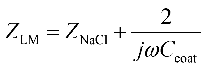 | (1) |
 | ||
| Fig. 2 A (a) cross-sectional electrical model of a LM and the overall circuit diagram of the detection system, and a (b) lumped equivalent circuit diagram. The AC power supply (Vs) is 20 V peak-to-peak and 10 MHz. The oscilloscope is connected to a computer via USB to measure the voltage amplitude across Rext (Vext). Not to scale. | ||
As explanation, if the LM sensor is considered to be acting purely as an impedance Zm, the circuit can be considered to be acting as a DC potential divider, and therefore would follow (2); where Vs is the applied voltage, Vext is the voltage across the external resistor, Zm is the impedance of the LM and PCB wires, and Rext is the resistor.
 | (2) |
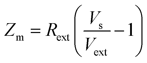 | (3) |
The value of Zm calculated using eqn (3) — rearranged from eqn (2) — includes both the LM and parasitic PCB impedance. In order to remove the PCB impedance, separate measurements were taken: (a) with a short-circuit sensor, and (b) with open-circuit sensor without a LM on the sensor. The impedance of the LM can therefore be given by:
 | (4) |
4 Results & discussion
4.1 Capacitance of a liquid marble
In order to gauge the actual capacitance of the LMs in the system, a standard square wave was applied to the system. To measure the current a shunt resistor was used, and the potential drop across it measured. The applied square wave had Vp–p = 4 V, DC offset = 0 V, f = 100 kHz. This was performed both in the presence and absence of a saturated NaCl(aq) 30 μL PE LM, in order to ascertain the parasitic capacitance of the system. The resulting plot, in the presence of a LM, can be seen in Fig. 3. | ||
| Fig. 3 The charging/discharging cycle of the LM capacitor, as measured by the voltage across Rext, at Vp–p = 4 V, DC offset = 0 V, f = 100 kHz. This is proportional to the current through the resistor. | ||
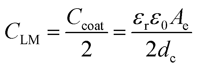
It is possible to calculate capacitance using the plots in Fig. 3 by measuring the time taken to reach one time constant: the time taken to reach 63.2% of the capacitors full charge. This can then be used to calculate the capacitance of the system using C = t/R, where t is the time constant. The capacitance of the empty system is the parasitic capacitance, Cpara, which when subtracted from the capacitance of the measured LM system Cm gives the capacitance of the LM in the system, CLM: such that Cm = Cpara + CLM. Note that Cpara = Cww + Cwg, and CLM = Ccoat/2. The measured value of capacitance was CLM = 0.10 pF. This value was compared to a simulated system, where twin capacitors were considered in series. By knowing the electrode contact area, it is possible to calculate the expected capacitance using eqn (5), where εr is the relative permittivity (dielectric constant) of the powder coating, ε0 is the permittivity of free space, Ae is the electrode plate area, and dc is the thickness of the LM's powder coating. The integer divisor is required as the system acts as two capacitors in series: first going across the powder coating into the LM, and second going back across the coating out of the LM.
 | (5) |
The calculated value for the system is 0.12 pF, which is in good agreement with the measured value. It is worth noting that an equivalent simplified circuit model can be envisaged, by replacing the twin capacitors with a single capacitor that has double the coating particle diameter (spacing between electrodes).
4.2 Response to the particle size of a liquid marble coating
In order for this system to be useful for a variety of liquid marbles and resulting applications, the system should not be restricted by the size of the particles chosen for the powder coating of the LM. Therefore, the sensor grid, described in section 2, was tested using both 30 μL and 50 μL LMs with various particle sizes and a saturated NaCl aqueous core. The results can be seen in Fig. 4(a). The solid markers indicate PE LMs, whilst the hollow markers are PTFE LMs; red squares indicate 30 μL LMs, and blue triangles show 50 μL LMs. The black dashed line with zero gradient indicates the voltage amplitude across the resistor in the absence of a LM, with the red dotted lines either side indicating error. All error is the standard deviation of 10 measurements, with each measurement being the mean of 20 individual values. Note that none of the measurements, or the corresponding error, is near the level of the absent LM. | ||
| Fig. 4 (a) The amplitude of the AC signal recorded across the resistor, is plotted against the particle size of the powder coating of the LM. Solid red squares indicate a 30 μL PE coating, hollow red squares indicate a 30 μL PTFE coating, solid blue triangles show a 50 μL PE coating, and hollow blue triangles indicate a 50 μL PTFE coating. The dashed black line shows the signal when there is no LM present, and the red dotted line shows its error. All errors are standard deviations over 10 independent measurements. (b) The amplitude of the AC signal recorded across the resistor, is plotted against different concentrations of NaCl. Red squares indicate a 30 μL LM, and blue triangles indicate a 50 μL LM. The solid red line is a linear line of best fit, with an R-squared of 0.996, and the dashed blue line is a linear line of best fit, with an R-squared of 0.977. Plots are averages of 10 measurements, and errors are standard deviations over said 10 independent measurements. (c) The amplitude of the AC signal recorded across the resistor, is plotted against the volume of different LMs. Red squares indicate a concentrated NaCl(aq) core, and blue triangles indicate a DIW core. The solid red line is a linear line of best fit, with an R-squared of 0.992, and the dashed blue line is a linear line of best fit, with an R-squared of 0.991. Plots are averages of 10 measurements, and errors are standard deviations over said 10 independent measurements. (d) The amplitude of the AC signal recorded across the resistor, using a single pin of the sensor grid, is plotted against the pin's physical location. The black dashed line shows the sensor with no LM, and the red line shows the presence of a 30 μL PTFE LM made with a 25 wt% NaCl solution. Each point is an average of 10 measurements, and error bars are standard deviations over said 10 measurements. The x-axis indicates the respective electrical trace's distance from the centre of the sensor. | ||
Importantly, the sensor functions as desired for all tested particle sizes and volumes. There is minimal variance between repeated tests of the same particle sizes, though there is variation across different particle sizes. Despite the slight polydisperse nature of the powder, a clear trend can be seen: as the particle size of the LMs powder coating increases, the signal decreases. This is due to the affected impedance of the capacitive sensor. In the absence of a LM, the applied AC current passes through the parasitic capacitance of the electrodes which results in a larger voltage drop across the sensor. When a LM is placed on top of the sensor, a new route is available. The AC current can pass up into the LM, through the core, and back down to the grounded side of the circuit, thus completing it. This new pathway is lower in impedance than the previous path, and so the voltage drop across the capacitor decreases. This causes a consequent increase of potential across the resistor, which is measured using an oscilloscope. The larger LMs cause a greater signal amplitude, which is to be expected, as the larger LMs cover more of the sensor grid. This is discussed fully in section 4.4.
The trend in signal amplitude is due to the different LM coating thickness, which relates to particle size. As described in section 3, the coating around LM can be modelled as a capacitance (Ccoat) and it is inversely proportional to the coating thickness. As the coating thickness increases, Ccoat decreases (see eqn (5)). Therefore, according to eqn (1), ZLM increases. Due to eqn (2), the increasing ZLM reduces the signal amplitude (Vext) which is measured across Rext.
It is interesting to note that the PTFE LMs (hollow markers in Fig. 4(a)) are in line with the PE LMs. The larger signal amplitude is due to the smaller particle size of the PTFE powder, and so the reduced coating. This suggests that the powder coating is not greatly interacting with the sensor. There are two reasons for this: firstly, relative permittivities of PE and PTFE are very similar;38 and secondly, the powder coating of the LM occupies a small amount of the current pathway, approximately 100 μm twice, compared to hundreds of microns through the core of the LM, as the current has many different grounding points.
4.3 Response to the salt concentration of a liquid marble
Due to the nature of the sensor, the output signal is dependent on the electrical conductivity of the LM's core. Therefore, investigations were performed on the sensitivity of the sensor to cores of different conductivities. The conductivity of aqueous NaCl solutions increases linearly with concentration,38 and so was deemed a suitable candidate. Various concentrations of NaCl solutions were tested using both 30 μL and 50 μL PTFE LMs, in order to discover any trend. The results of which can be seen in Fig. 4(b).For the 30 μL LMs (red squares), there is a clear strong relationship between the NaCl concentration inside the LM, and the amplitude of the signal. A linear relationship can be extrapolated, yielding the equation V = 4.97 × 10⁻⁴·[NaCl] + 0.322. This function has been plotted on the graph as a solid red line, and has an R-squared of 0.996. Such a relationship is expected, as the conductivity of NaCl in water also increases proportionally with concentration, due to its complete dissociation when solvated.38 It therefore follows the proportionality of resistance, R ∞ l/σA, where l is the length of the ‘resistor’, σ is its conductivity, and A is its cross sectional area. Due to these effects, ZNaCl reduces as the NaCl concentration increases the reduction in ZNaCl reduces ZLM and so increases Vext, the signal amplitude.
The larger LMs (blue triangles) also follow a similar linear trend, with the equation V = 5.55 × 10⁻⁴·[NaCl] + 0.331. This function has also been plotted on the graph, as a blue dashed line, and has an R-squared of 0.977. The larger LMs result in a greater signal amplitude than the smaller LMs, this is because the larger LMs cover more of the sensor grid. This is discussed fully in section 4.4.
It should be noted that changes in the salt concentration would have an effect on the surface tension of the aqueous core,39 which would in turn affected the shape of the LM. However, any such change in the LM shape (and ensuing contact area with the sensor) are accounted for. As the relationship shown in Fig. 4(b) uses empirical data, any changes in LM shape are incorporated by design.
This relationship makes it possible to not only use the sensor to detect the presence or absence of a LM, but also to gain useful characteristic data on it. This has many applications, including potential determination of the concentration of the cargo inside a LM, without interfering with said cargo, which is useful in microfluidics. For example, when the progress of a reaction needs to be monitored, but there is a desire to not directly interact with the reaction. Contactless determination of the LM's cargo concentration also allows for fast and clean measurements: there are no probes to place inside the LM, and so no time-consuming cleaning after the measurement, and therefore no risk of contamination with the next LM to be tested.
4.4 Response to the volume of a liquid marble
Investigations were also conducted on the susceptibility of the sensor to the volume of a LM. Tests were performed using a PTFE powder coating and both a DIW and saturated NaCl aqueous core. LMs were tested from 2.5 μl up to 100 μl in 5 μl and 10 μl steps (no cracking in the powder coating was observed for the larger LMs, the size restriction was the physical dimensions of our sensor). Each volume was tested 10 times. The results of which are presented in Fig. 4(c).It can be seen that there is a strong positive relationship between the volume of the LM and the signal amplitude: the signal amplitude increases with increasing volume of the liquid marble. This is true for both the DIW (blue triangles) and saturated NaCl (red squares) LMs. This relationship is due to two main factors: the increase in amount of the LM in contact with the sensor and the reduction of ZNaCl. The LM, being soft, does not rest on a spherical bottom point, but instead sits on a flattened out base, visible in Fig. 1(c). It is this base which increases with size as the LM volume is increased. As the base increases in size, additional electrical traces in the sensor are in contact with the LM, allowing more current to pass into and exit the LM. Further, since there is more liquid volume, the cross-sectional area for the current path is significantly higher compared to smaller LMs. These two factors lower the impedance of the sensor and thereby its potential drop, again due to the proportionality of resistance.
As expected, and as previously explained in section 4.3, the saturated NaCl(aq) LMs have a greater signal amplitude at a fixed volume. The gradient is slightly different between the two cores however: 5.01 × 10⁻⁴ for DIW and 5.58 × 10⁻⁴ for NaCl(aq). This is explained by the greater conductivity of the NaCl(aq) LMs permitting more effective use of the entire of the cross-section of the LM, as opposed to DIW LMs whose lower core conductivity restricts effective signal conduction to regions closer to the bottom of the LM (and thereby closer to the sensor traces).
The phenomenon of maximal LM height plays a role in the linear nature of the plot in Fig. 4(c). As the volume of the LM increases, it reaches a maximal height in a logarithmic manner,40 resultantly the breadth of the LM increases disproportionally with its volume (a cartoon demonstration is shown in Fig. 5(a)). The contact radius of variously sized LMs was measured using light microscopy by observing where the powder particles moved out of the focal plane (as explained in the Experimental section), an example image of which is shown in Fig. 5(b). The contact area was then calculated using circle theory and plotted against LM volume, shown in Fig. 5(c).
 | ||
| Fig. 5 (a) A sketch of a LM resting on the sensor, demonstrating how the height of an expanding LM plateaus as the volume is increased, causing the breadth of a LM to increase disproportionately. Not to scale. (b) A collection of 9 light microscope images stitched together, providing a ‘bottom-up’ view of a LM. This facilitated measurement of the contact diameter of the LM (a 10 μL PTFE DIW LM in the example image). The contact diameter can be determined by observing where the powder particles move out of the focal plane. The scale bar is 500 μm. (c) The contact area of a LM against its volume. Error bars indicate the mean absolute deviation. LMs had a PTFE powder coating and a deionised water core. The dashed red line indicates the positive growth phase where the contact area is proportional to V4/3, and the dotted blue line indicates the region where the LMs maximal height results in the contact area becoming linearly proportional to V. Both fittings were first introduced for LMs by Aussillous and Quéré.1,6 | ||
The contact area of differently sized LMs was first discussed by Aussillous and Quéré in 2001, and then again in 2006.1,6 They noted that for smaller LMs the contact radius, l, could be defined as  . Where R is the radius of the idealised spherical droplet; and the capillary length, λ, is defined as
  , where γ is the surface tension, ρ is the density, and g is gravitational acceleration. When related to contact area and LM volume, V, a relationship is revealed where the contact area is proportional to V4/3. This has been added to Fig. 5(c) as a red dashed line.
Once the volume of a LM is above a certain threshold, the mass of the liquid causes the height to plateau, typically at twice the capillary length. At this stage, as also reported by Aussillous and Quéré,1,6 the contact area increase is no longer polynomial. The contact radius of a larger LM can therefore be defined by  . When this is related to contact area and LM volume, it reveals that the contact area is linearly proportional to volume. This relationship is displayed in Fig. 5(c) as a blue dotted line. It is this linear relationship that dominates the volume-sensor response plot in Fig. 4(c).
4.5 Determining the location of a liquid marble
In order to ascertain location information of the LM from the sensor, each single trace on one side of the sensor was energised individually, whilst the other side remained as a single network of 18 traces connected to ground via Rext. The outer traces on each side were not used, as their asymmetry could skew the data. Fig. 4(d) demonstrates the location data obtained from the sensor. It can be clearly seen that there is a noticeable difference between the signal amplitudes in the range between pins 4 and 10, indicating the location of the LM on the sensor grid. This system can be used to determine the location of a LM in an environment, without directly interfering with the LM, with an accuracy equivalent to the spacing of the excitation electrical traces: 400 μm. There is also scope to measure the size of the LM, by inferring its diameter from the contact area. Due to variations with contact angles, this would require calibrating for each LM species.Measurement resolution of the device can be further improved by applying higher voltages, higher frequencies or a smoother sinusoidal waveform, as the capacitive reactance of the components is inversely proportional to the frequency of the applied signal, and therefore decreases. The frequency can be increased significantly, for example CPUs operating at 100 MHz have been available for decades. Testing has also revealed that the voltage can be greatly increased using the current sensor setup. On connecting two adjacent pins (100 μm apart) and ramping the DC potential, no breakdown (indicated by a drop in resistance) of the PCB was detected, within the limits of the SourceMeter (210 V, >200 MΩ). Therefore, it is possible to increase the voltage to 200 Vp–p and the frequency to 100 MHz, resulting in an increase of two orders of magnitude on excitation.
4.6 Dynamic measurements of a mobile liquid marble
A series of proof-of-principle measurements were also made of liquid marbles dynamically rolling across the sensor grid. LMs comprised of a 25 wt% NaCl aqueous core and PTFE coating were used. These measurements recorded the signal amplitude of each waveform, and plotted a smoothed signal amplitude with averaging over 250 μs. As the LM approached the sensor the signal increases, reaching a maximum when the LM is entirely covering the sensor, then returning to its baseline level once the LM has left the sensor. Plots showing the traversing of a single LM, and of two separate LMs, can be seen in Fig. 6(a) and (b), respectively.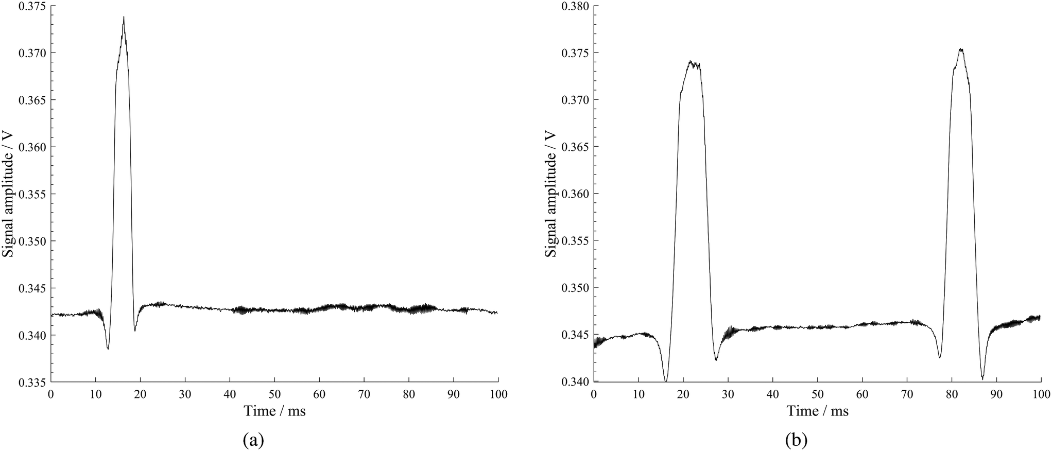 | ||
| Fig. 6 Signal amplitude plots showing the traversing of (a) one, and (b) two LMs across the sensor. The time for each of these LMs to traverse the sensor was 7 ms to 12 ms, with speeds of 1.0 m s−1 to 1.9 m s−1. | ||
As long as the sensor grid is wider than the contact length of the LM, then it is possible to calculate the speed of the LM, from the breadth of the signal peak. The leading edge of the LM entering the sensor causes the signal to start to increase, and the leading edge of the LM leaving the sensor causes the signal to begin to decrease. For peaks of this style, the start of the peak rise to the start of the peak decrease is equivalent to the full-width at half-maximum (FWHM), which provides a time. By knowing the width of the sensor (7.1 mm) it is possible to calculate the speed of the LMs in the above plots. The LM in Fig. 6(a) had a speed of 2.0 m s−1, the first LM in Fig. 6(b) had a speed of 1.0 m s−1, whilst the second LM in that figure had a speed of 1.1 m s−1. This assumes a steady speed across the 7.1 mm of the sensor.
4.7 Application to computing
Unconventional computing has previously exploited the properties of LMs,9,27,41 facilitating their use as both a signal and signal carrier. The capability of the system to detect the position and volume of a LM permits the use of a new and facile system of addition and division. Using the sensor grid, we have demonstrated how the volume of a LM can be measured with ease. When two LMs are coalesced9,29 then their volumes are added, and the volume of the new LM can be determined. Additionally, by splitting the LM into smaller separate LMs (possible using previously published techniques30,42,43), the physical division can be measured quantitatively, to determine the comparable mathematical division.In the billiard-ball style of computing44–46 it is possible to fuse signals (LMs) in a collision, and thereby implement logic gate 〈x, y〉 → 〈![[x with combining macron]](https://www.rsc.org/images/entities/i_char_0078_0304.gif) y, xy, xȳ〉. The resulting larger volume of the new signal would be confirmation that such an operation had been performed. Conservative logic requires that the output signal be identical to the input, and so the design would need to be supplemented with a LM divider (as previously mentioned) to return the signal to its original volume. It would also be possible to implement either a more traditional billiard-ball gate or a Margolus logic gate — 〈x, y〉 → 〈y, xy, xy, xȳ〉 — where the signals collide and rebound, rather than fuse. In such a system, our sensor could not only be used to measure the size and speed of the colliding LMs, but an appropriately positioned sensor grid could also determine directional information of the rebounding marbles.
y, xy, xȳ〉. The resulting larger volume of the new signal would be confirmation that such an operation had been performed. Conservative logic requires that the output signal be identical to the input, and so the design would need to be supplemented with a LM divider (as previously mentioned) to return the signal to its original volume. It would also be possible to implement either a more traditional billiard-ball gate or a Margolus logic gate — 〈x, y〉 → 〈y, xy, xy, xȳ〉 — where the signals collide and rebound, rather than fuse. In such a system, our sensor could not only be used to measure the size and speed of the colliding LMs, but an appropriately positioned sensor grid could also determine directional information of the rebounding marbles.
Computation can also be achieved by coalescing LMs with cores of different concentrations, to form a new combined core which has a concentration determined by the values of the original inputs. The properties of the new core (including concentration and size) can be measured using the techniques covered in this paper. This enables a new direction in computation to be explored. We performed a preliminary billiard-ball collision experiment by colliding two 20 μL PTFE LMs to yield a single 40 μL PTFE LM. The reported sensor successfully recorded the volumes of both the starting LMs, and the resulting larger LM — indicating a successful coalescence.
Capacitance of LMs could be applied in design of flexible and stretchable logical circuits47–49 and soft robotics,50 especially where disposable devices are used. Capacitive threshold logic51 is an extension of standard threshold logic, wherein logical values 1 and 0 are interpreted from the voltage being above or below a certain value. It can also be used to design capacitive synapse architecture.52,53 The easily variable capacitance of the LM sensor system (through the addition or removal of LM volume), permits straightforward tuning of the set-up.
It is worth noting that the evaporation of LMs would need to be controlled in a computing environment. Several previous studies have investigated the evaporation of LMs,12–15,54,55 and the rate has been shown to be related to several factors, including the powder coating, initial volume, and ambient humidity. Limiting the evaporation of LMs by maintaining a high-humidity environment has been previously demonstrated with success.56
5 Conclusions
Herein is reported a novel LM sensor, constructed using standard PCB manufacturing techniques and operating with 20 Vp–p at 10 MHz. The sensor is low-cost and scalable, allowing future projects to have many large (or small) sensors. As the LM rests on the sensor, the change in impedance (comprised of the electrical resistance, capacitive reactance and inductive reactance) causes a measurable change in the current following through the accompanying circuit. This change was quantified using a digital oscilloscope, and was found to correlate to many identifiable features of the present LM. Using this system, we have demonstrated the contactless and non-invasive measurement of a number of LM properties: (1) particle size of the LM coating, (2) the concentration of a NaCl solution used as the LM core, (3) the volume of the LM, and (4) the accurate positioning of the LM. These properties are vital to LM systems, especially automatic LM makers. Sensing has been performed under both static and dynamic conditions.The ability to automatically detect the volume of a LM in a non-destructive and contactless manner has many potential uses, especially in pharmaceutical manufacturing processes and biomedical diagnostic testing due to benefits associated with self-contained small sample volume bioreactors.57 It should be noted that this technique distinguishes between LMs and a naked droplet of equivalent mass (unlike a balance). There are now several papers that address the facile and automatic formation of LMs,9,30,58 and so having a method for easy confirmation that each LM formed is within required tolerance limits is certainly advantageous.
Conflicts of interest
There are no conflicts of interest to declare.Acknowledgements
The authors thank Matthew Stevens for fruitful & constructive discussions, and Dr David Patton of the University of the West of England for help with SEM imaging. TCD, CF, BPJDLC, and AA acknowledge support from the EPSRC with grant EP/P016677/1. RW acknowledges support from the UWE Bristol Vice Chancellor's Early Career Research Award. This work was conducted entirely at the University of the West of England, Bristol, UK.References
- P. Aussillous and D. Quéré, Proc. R. Soc. A, 2006, 462, 973–999 CrossRef CAS.
- G. McHale and M. I. Newton, Soft Matter, 2015, 11, 2530–2546 RSC.
- Y. Zhang and N.-T. Nguyen, Lab Chip, 2017, 17, 994–1008 RSC.
- N. M. Oliveira, R. L. Reis and J. F. Mano, Adv. Healthcare Mater., 2017, 6, 1700192 CrossRef PubMed.
- R. Mayne, T. C. Draper, N. Phillips, J. G. H. Whiting, R. Weerasekera, C. Fullarton, B. P. J. de Lacy Costello and A. Adamatzky, Langmuir, 2019, 35, 13182–13188 CrossRef CAS PubMed.
- P. Aussillous and D. Quéré, Nature, 2001, 411, 924–927 CrossRef CAS PubMed.
- N.-T. Nguyen, M. Hejazian, C. Ooi and N. Kashaninejad, Micromachines, 2017, 8, 186 CrossRef.
- T. Arbatan, L. Li, J. Tian and W. Shen, Adv. Healthcare Mater., 2012, 1, 80–83 CrossRef CAS.
- T. C. Draper, C. Fullarton, N. Phillips, B. P. de Lacy Costello and A. Adamatzky, Mater. Today, 2017, 20, 561–568 CrossRef CAS.
- C. Fullarton, T. C. Draper, N. Phillips, B. P. J. de Lacy Costello and A. Adamatzky, J. Phys. Mater., 2019, 2, 015005 CrossRef.
- A. Adamatzky, C. Fullarton, N. Phillips, B. De Lacy Costello and T. C. Draper, R. Soc. Open Sci., 2019, 6, 190078 CrossRef.
- M. Dandan and H. Y. Erbil, Langmuir, 2009, 25, 8362–8367 CrossRef CAS PubMed.
- H. Y. Erbil, Adv. Colloid Interface Sci., 2012, 170, 67–86 CrossRef CAS PubMed.
- C. Fullarton, T. C. Draper, N. Phillips, R. Mayne, B. P. J. de Lacy Costello and A. Adamatzky, Langmuir, 2018, 34, 2573–2580 CrossRef CAS PubMed.
- F. Geyer, Y. Asaumi, D. Vollmer, H.-J. Butt, Y. Nakamura and S. Fujii, Adv. Funct. Mater., 2019, 1808826 CrossRef.
- T. Thorsen, R. W. Roberts, F. H. Arnold and S. R. Quake, Phys. Rev. Lett., 2001, 86, 4163–4166 CrossRef CAS PubMed.
- R. B. Fair, Microfluid. Nanofluid., 2007, 3, 245–281 CrossRef CAS.
- Z. Guttenberg, H. Müller, H. Habermüller, A. Geisbauer, J. Pipper, J. Felbel, M. Kielpinski, J. Scriba and A. Wixforth, Lab Chip, 2005, 5, 308–317 RSC.
- A. A. Darhuber, J. P. Valentino, J. M. Davis, S. M. Troian and S. Wagner, Appl. Phys. Lett., 2003, 82, 657–659 CrossRef CAS.
- E. Ghafar-Zadeh, M. Sawan and D. Therriault, Sens. Actuators, A, 2008, 141, 454–462 CrossRef CAS.
- C. Elbuken, T. Glawdel, D. Chan and C. L. Ren, Sens. Actuators, A, 2011, 171, 55–62 CrossRef CAS.
- A. Kalantarifard, A. Saateh and C. Elbuken, Chemosensors, 2018, 6, 23 CrossRef.
- J. Z. Chen, A. A. Darhuber, S. M. Troian and S. Wagner, Lab Chip, 2004, 4, 473–480 RSC.
- C. A. Merten, H. Hu and D. Eustace, WO Pat. 2016/174229/A1, 2016 Search PubMed.
- X. Fu, Y. Zhang, H. Yuan, B. P. Binks and H. C. Shum, ACS Appl. Mater. Interfaces, 2018, 10, 34822–34827 CrossRef CAS PubMed.
- J. Jin, C. H. Ooi, K. R. Sreejith, D. V. Dao and N.-T. Nguyen, Phys. Rev. Appl., 2019, 11, 044059 CrossRef CAS.
- T. C. Draper, C. Fullarton, N. Phillips, B. P. J. de Lacy Costello and A. Adamatzky, Sci. Rep., 2018, 8, 14153 CrossRef PubMed.
- J. Jin, C. H. Ooi, D. V. Dao and N.-T. Nguyen, Soft Matter, 2018, 14, 4160–4168 RSC.
- T. C. Draper, C. Fullarton, R. Mayne, N. Phillips, G. E. Canciani, B. P. J. de Lacy Costello and A. Adamatzky, Soft Matter, 2019, 15, 3541–3551 RSC.
- B. Wang, K. F. Chan, F. Ji, Q. Wang, P. W. Y. Chiu, Z. Guo and L. Zhang, Adv. Sci., 2019, 1802033 CrossRef PubMed.
- Z. Chen, D. Zang, L. Zhao, M. Qu, X. Li, X. Li, L. Li and X. Geng, Langmuir, 2017, 33, 6232–6239 CrossRef CAS PubMed.
- Z. Liu, X. Fu, B. P. Binks and H. C. Shum, Soft Matter, 2017, 13, 119–124 RSC.
- Z. Liu, T. Yang, Y. Huang, Y. Liu, L. Chen, L. Deng, H. C. Shum and T. Kong, Adv. Funct. Mater., 2019, 29, 1901101 CrossRef.
- Y. Zhang, X. Fu, W. Guo, Y. Deng, B. P. Binks and H. C. Shum, Lab Chip, 2019, 19, 3526–3534 RSC.
- S. Preibisch, S. Saalfeld and P. Tomancak, Bioinformatics, 2009, 25, 1463–1465 CrossRef CAS PubMed.
- J. Schindelin, I. Arganda-Carreras, E. Frise, V. Kaynig, M. Longair, T. Pietzsch, S. Preibisch, C. Rueden, S. Saalfeld, B. Schmid, J.-Y. Tinevez, D. J. White, V. Hartenstein, K. Eliceiri, P. Tomancak and A. Cardona, Nat. Methods, 2012, 9, 676–682 CrossRef CAS PubMed.
- C. T. Rueden, J. Schindelin, M. C. Hiner, B. E. DeZonia, A. E. Walter, E. T. Arena and K. W. Eliceiri, BMC Bioinf., 2017, 18, 529 CrossRef PubMed.
- CRC Handbook of Chemistry and Physics: Student, ed. R. C. Weast, CRC Press, Boca Raton, Florida, USA, 1st edn, 1988, pp. D105–E49 Search PubMed.
- H. Chen, Z. Li, F. Wang, Z. Wang and H. Li, J. Chem. Eng. Data, 2017, 62, 3783–3792 CrossRef CAS.
- E. Bormashenko, R. Pogreb, G. Whyman and A. Musin, Colloids Surf., A, 2009, 351, 78–82 CrossRef CAS.
- T. C. Draper, C. Fullarton, N. Phillips, B. P. J. de Lacy Costello and A. Adamatzky, in UCNC 2018, LNCS 10867, ed. S. Stepney and S. Verlan, Springer, 2018, pp. 59–71 Search PubMed.
- E. Bormashenko and Y. Bormashenko, Langmuir, 2011, 27, 3266–3270 CrossRef CAS PubMed.
- V. Sivan, S.-Y. Tang, A. P. O'Mullane, P. Petersen, N. Eshtiaghi, K. Kalantar-zadeh and A. Mitchell, Adv. Funct. Mater., 2013, 23, 144–152 CrossRef CAS.
- T. Toffoli, in Int. Colloq. Autom. Lang. Program., ed. J. de Bakker and J. van Leeuwen, Springer, 1980, pp. 632–644 Search PubMed.
- E. Fredkin and T. Toffoli, in Collision-Based Computing, ed. A. Adamatzky, Springer, London, 2002, pp. 47–81 Search PubMed.
- N. Margolus, in Collision-Based Computing, ed. A. Adamatzky, Springer, London, 2002, pp. 107–134 Search PubMed.
- L. Cai and C. Wang, Nanoscale Res. Lett., 2015, 10, 320 CrossRef PubMed.
- J. A. Rogers, T. Someya and Y. Huang, Science, 2010, 327, 1603–1607 CrossRef CAS PubMed.
- G. Cantarella, C. Vogt, R. Hopf, N. Münzenrieder, P. Andrianakis, L. Petti, A. Daus, S. Knobelspies, L. Büthe, G. Tröster and G. A. Salvatore, ACS Appl. Mater. Interfaces, 2017, 9, 28750–28757 CrossRef CAS.
- S. Kim, C. Laschi and B. Trimmer, Trends Biotechnol., 2013, 31, 287–294 CrossRef CAS.
- H. Ozdemir, A. Kepkep, B. Pamir, Y. Leblebici and U. Cilingiroglu, IEEE J. Solid-State Circuits, 1996, 31, 1141–1150 CrossRef.
- U. Cilingiroglu, in Int. Symp. Circuits Syst., IEEE, 1990, pp. 2982–2985 Search PubMed.
- U. Cilingiroglu, IEEE Trans. Circuits Syst., 1991, 38, 210–217 CrossRef.
- C. H. Ooi, E. Bormashenko, A. V. Nguyen, G. M. Evans, D. V. Dao and N.-T. Nguyen, Langmuir, 2016, 32, 6097–6104 CrossRef CAS.
- K. R. Sreejith, C. H. Ooi, D. V. Dao and N.-T. Nguyen, RSC Adv., 2018, 8, 15436–15443 RSC.
- K. R. Sreejith, L. Gorgannezhad, J. Jin, C. H. Ooi, H. Stratton, D. V. Dao and N.-T. Nguyen, Lab Chip, 2019, 19, 3220–3227 RSC.
- R.-E. Avrămescu, M.-V. Ghica, C. Dinu-Pîrvu, D. I. Udeanu and L. Popa, Molecules, 2018, 23, 1120 CrossRef.
- K. R. Sreejith, C. H. Ooi, J. Jin, D. V. Dao and N.-T. Nguyen, Rev. Sci. Instrum., 2019, 90, 055102 CrossRef PubMed.
Footnotes |
| † Electronic supplementary information (ESI) available. See DOI: 10.1039/c9lc01001g |
| ‡ Current address: Department of Earth and Planetary Sciences, Harvard University, 20 Oxford Street, Cambridge, MA 02138, USA. |
| This journal is © The Royal Society of Chemistry 2020 |