
 Open Access Article
 This Open Access Article is licensed under a
 Creative Commons Attribution 3.0 Unported Licence
Efficient NO2 sensing performance of a low-cost nanostructured sensor derived from molybdenite concentrate†
Mirabbos
Hojamberdiev
 *a,
Neeraj
Goel
b,
Rahul
Kumar
b,
Zukhra C.
Kadirova
c and
Mahesh
Kumar
b
*a,
Neeraj
Goel
b,
Rahul
Kumar
b,
Zukhra C.
Kadirova
c and
Mahesh
Kumar
b
aInstitut für Chemie, Technische Universität Berlin, Straße des 17. Juni 135, 10623 Berlin, Germany. E-mail: khujamberdiev@tu-berlin.de; Fax: +49 (0) 30 314-79656; Tel: +49 (0)30 314-26178
bDepartment of Electrical Engineering, Indian Institute of Technology Jodhpur, Jodhpur-342037, India
cDepartment of Inorganic Chemistry, Faculty of Chemistry, National University of Uzbekistan, University Street 4, 100174 Tashkent, Uzbekistan
First published on 7th September 2020
Abstract
Accumulation of industrial solid waste necessitates the development of utilization processes and technologies to reduce their negative environmental impact. Herein, molybdenite concentrate from the mining-metallurgy industry is systematically characterized as a valuable starting material for the fabrication of an efficient and low-cost nanostructured gas sensor. Few-layer MoS2 is obtained from molybdenite concentrate by liquid nitrogen exfoliation and deposited on different substrates by spin coating and drop casting. It is found that spin coating is advantageous over drop casting in fabricating a homogeneous and dense few-layer MoS2 film. The charge-transfer-based sensing performance of the fabricated few-layer MoS2 film is investigated upon exposure to NO2 at different temperatures (50, 100, and 120 °C). At an optimized temperature of 120 °C, a faster recovery is achieved, and the fabricated device exhibits 28, 38, and 44% sensitivity to 10, 50, and 100 ppm NO2, respectively, making it suitable for practical applications. Furthermore, the adsorption affinity of NO2 to the predominant (002) crystallographic plane of MoS2 is estimated from the distribution of field density and the calculated differential adsorption energies. According to the molecular modeling data, NO2 in the Ar/NO2 mixture has better interaction (dEad/dNNO2 = 4.77 kcal mol−1) with the few-layer MoS2 surface than individual NO2 (dEad/dNNO2 = 2.57 kcal mol−1), and van der Waals interaction (≈14 kcal mol−1) is the main adsorption force compared to the relatively weaker electrostatic interaction (<1 kcal mol−1). This work demonstrates a straightforward approach not only for the conversion of molybdenite concentrate into an efficient and low-cost nanostructured gas sensor but also for the reduction of the negative impact of accumulated molybdenum concentrate on the environment and human health.
1. Introduction
Rapid industrialization and urbanization have led to severe air pollution that has increasing negative impacts on human health and the environment alike. The United States Environmental Protection Agency (EPA) has even started an AirNow program that receives, manages and shares the data related to the real-time global air quality.1 This program also forecasts the local air quality and supports actions to reduce exposure to air pollution. Along with other hazardous air pollutants like sulfur dioxide (SO2), carbon dioxide (CO2), and nitrogen monoxide (NO), nitrogen dioxide (NO2) is emitted into the atmosphere as a product of combustion processes (vehicles, industry, heating, shipping, etc.)2 and explosives.3 NO2 is the main source of tropospheric ozone and PM2.5 and forms nitrous acid (acid rain) upon reaction with water, which is harmful to ecosystems. Short- and long-term exposure to NO2 can have adverse respiratory and cardiovascular health effects and even mortality.4 According to the current World Health Organization's guideline, the NO2 annual mean value has been set to 40 micrograms per cubic meter in order to protect public health.5 It is a prerequisite to constantly monitor the air quality using highly sensitive and fast gas sensing systems to comply with laws and regulations.In recent years, two-dimensional (2D) transition metal dichalcogenides, such as MoS2, MoSe2, WS2, WSe2, SnS2, etc., have gained enormous interest in sensing applications with low-power consumption due to their exceptional electrical, chemical, and physical properties.6 Among transition metal dichalcogenides, MoS2 has recently emerged as a potential candidate for NO2 sensing application due to its atomic-scale thickness, high surface to volume ratio, tunable band gap, and high on/off switching ratio.
A one-dimensional MoS2 nanowire network (NW) fabricated by using controlled turbulent vapor flow from the chemical transport reaction showed about 2-fold enhanced sensitivity for NO2 at 60 °C with a low detection limit (4.6 ppb) and enhanced sensitivity and selectivity towards NO2 because of a combination of abundant active edge sites and a large surface area and tuning of the potential barrier at the intersections of nanowires during adsorption/desorption.7 Vertically aligned MoS2 fabricated by using the rapid sulfurization method of CVD process showed about 5-fold enhanced sensitivity to NO2 compared to horizontally aligned MoS2 due to the high density of the exposed edge sites.8 Hierarchical MoS2 microsphere hollow structures synthesized by a hydrothermal method showed enhanced NO2 detection owing to the improved active edge sites.9 Some researchers have used a UV light source to improve the sensing performance of a MoS2 sensor at room temperature. For instance, a photoactivated mixed in-plane and edge-enriched p-type MoS2 flake-based sensor demonstrated a fast response with a good sensitivity of ∼10.36% for 10 ppm NO2 without and with complete recovery at room temperature and under UV light irradiation, respectively.10 Under photo excitation, MoS2 exhibited an enhanced sensitivity with ultrafast response time of ∼29 s and excellent recovery to NO2 (100 ppm) at room temperature due to charge perturbation on the surface of the sensing layer during the NO2/MoS2 interaction under light irradiation.11 A high-performance gas sensor prepared using a hybrid of temperature-assisted sulfur vacancy within the edge-oriented vertically aligned MoS2 and reduced graphene oxide exhibited a significantly enhanced response to NO2 with fast response and complete recovery due to the controlled electrical/chemical sensitization level of MoS2 through controllable vacancy and interface engineering.12
However, it is necessary to develop efficient and low-cost sensing materials based on MoS2 to find practical applications in NO2 sensing. One of the plausible ways to develop efficient and low-cost sensing materials is to utilize industrial solid wastes. In this work, we aim to characterize molybdenite concentrate from the mining-metallurgy industry and to fabricate an efficient and low-cost nanostructured sensor by utilizing molybdenite concentrate. Simple liquid nitrogen exfoliation is used to exfoliate few-layer MoS2 and to remove any impurities from molybdenite concentrate. The gas sensing behavior of the fabricated sensor by spin coating of few-layer MoS2 to the ppm concentration of NO2 is investigated. Furthermore, the adsorption affinity of NO2 to the predominant (002) crystallographic plane of molybdenite-2H is estimated from the distribution of field density and the calculated differential adsorption energies. This work demonstrates a straightforward approach not only for the conversion of molybdenite concentrate into an efficient and low-cost nanostructured gas sensor but also for the reduction of the negative impact of accumulated molybdenum concentrate on the environment and human health.
2. Experimental
2.1. Preparation
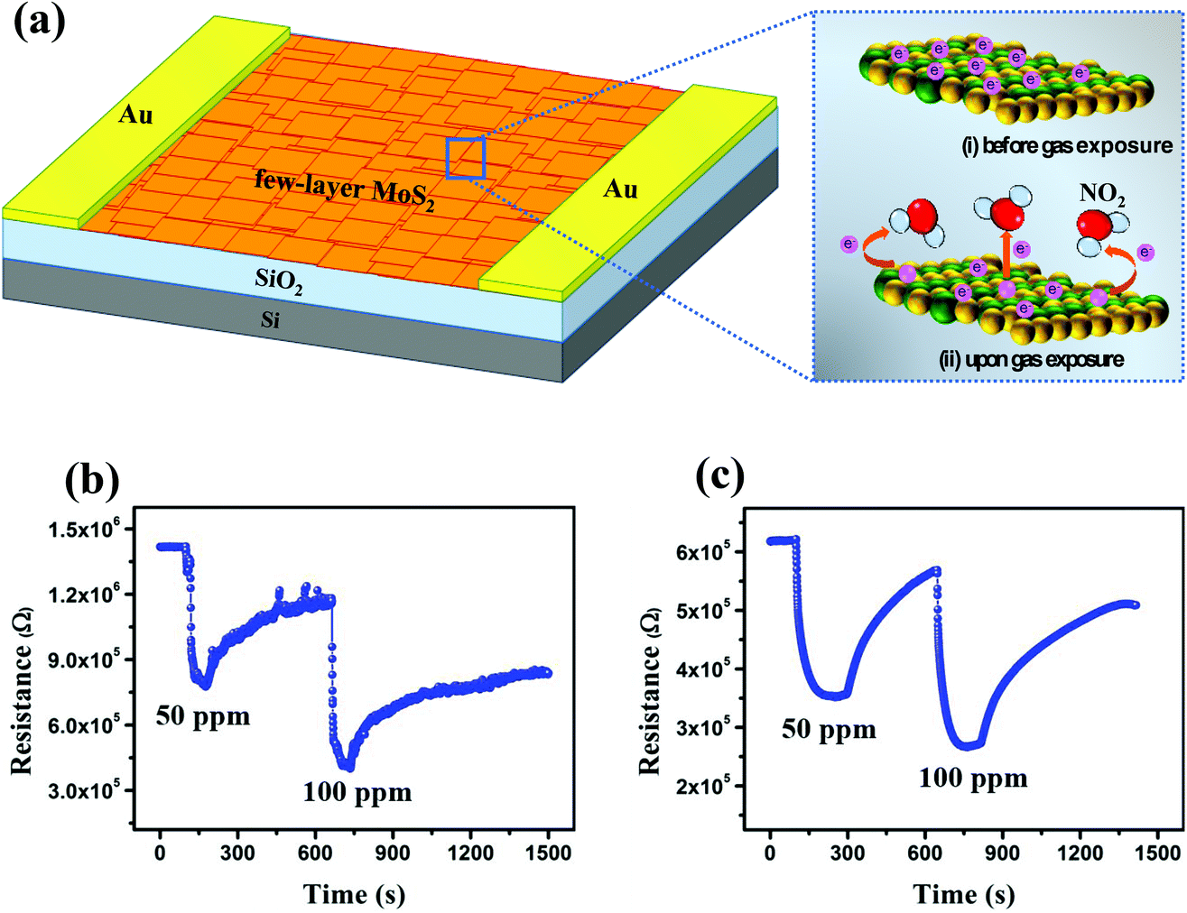
Molybdenite concentrate (MC) is generally formed during the extraction process of copper and molybdenum from porphyry copper-molybdenum in Almalyk Mining-Metallurgical Complex, Uzbekistan and has been used as the starting material in this study. As shown in Fig. 1, after grinding for 30 min, MC was immersed in liquid nitrogen for 2 h,13 and the upper part of the suspension was separated and ground again for 1 h. Afterward, 45 mg of the exfoliated MC was dispersed in 3 mL of isopropyl alcohol under sonication for 2 h. The samples were prepared by spin coating of the MC-based suspension on a SiO2/Si substrate at 1500 (MC1), 2500 (MC2) and 3500 (MC3) rpm for 30 s. The MC4 and MC5 samples were prepared by spin coating of the MC-based suspension on an n-type silicon substrate at 500 and 1500 rpm for 30 s, respectively. The MC6 sample was prepared by drop casting of 30 μL of the MC-based suspension on a metallic IDC-patterned SiO2/Si substrate.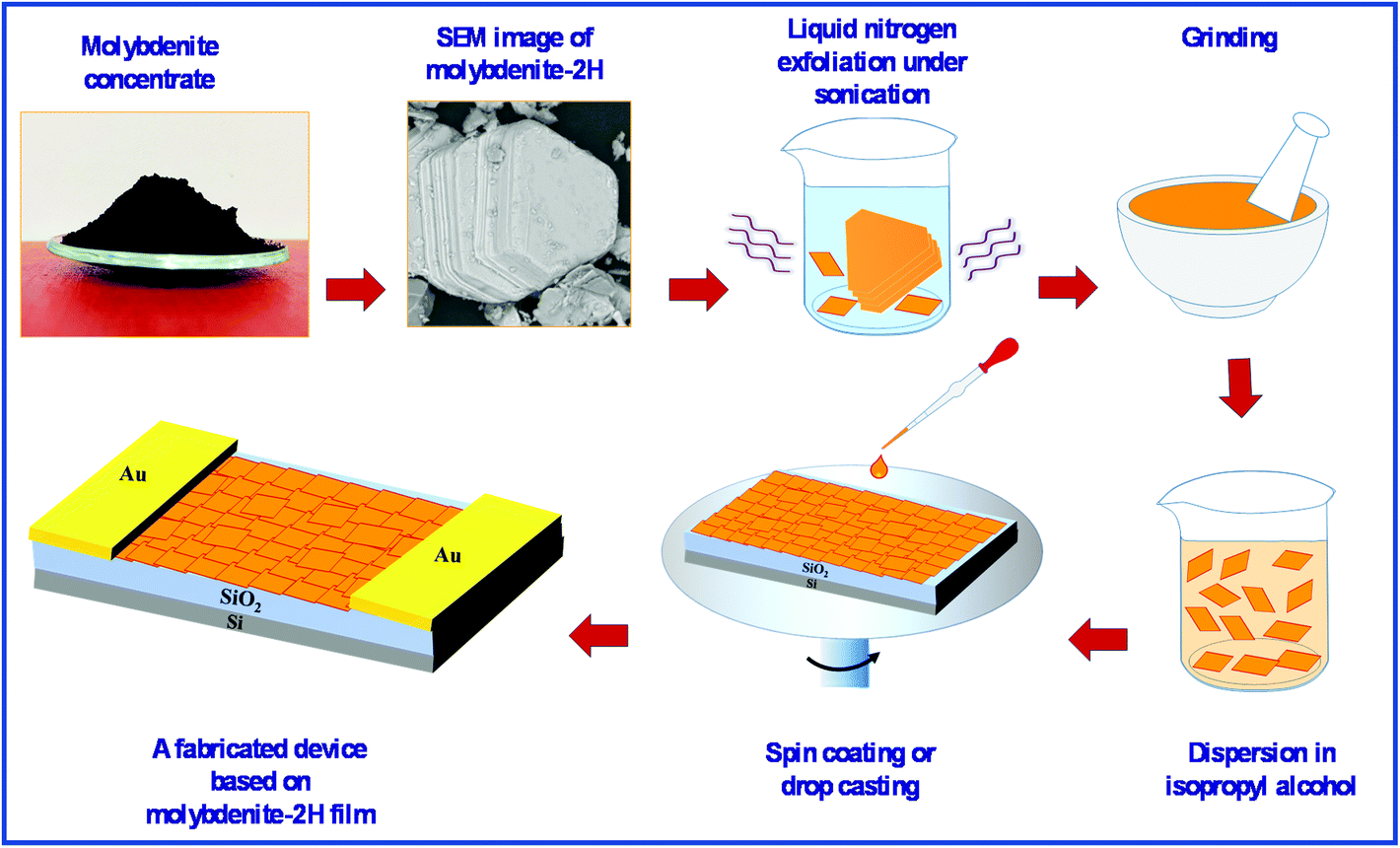 | ||
| Fig. 1 Preparation procedure of a low-cost nanostructured sensor from molybdenite concentrate. | ||
The conductivity of the fabricated sensing device is very important in examining its sensing response. Previously, it has been reported that few-layer MoS2 has higher conductivity than its monolayer and multilayer counterparts.14 Therefore, we have used few-layer MoS2 to fabricate a sensing device that shows a higher sensing response stability while maintaining a high surface to volume ratio. The fabricated sensing device was annealed at 300 °C for 1 h under a N2 atmosphere to reduce the unintentional barrier at the metal/semiconductor interfaces.15 Au was used to create an Ohmic contact with few-layer MoS2.16,17 The current–voltage characteristic curve of the fabricated sensing device at room temperature is shown Fig. S1 in the ESI,† indicating the Ohmic behavior of the fabricated sensing device.
2.2. Characterization
The X-ray diffraction (XRD) patterns were recorded on a MiniflexII (Rigaku) diffractometer using Cu Kα radiation (λ = 0.15418 nm) in the 2θ scan range from 10 to 80°. The morphology of the samples was examined using a JSM-7600F field-emission-type scanning electron microscope (JEOL). The energy-dispersive X-ray spectroscopy (EDX) element mapping images were obtained using a spectrometer attached to the SEM. The crystallinity and nanostructure of the samples were analyzed using a JEM-2100F HK high-resolution analytical scanning transmission electron microscope (JEOL). The ultraviolet-visible (UV-vis) diffuse reflectance spectrum of the samples was recorded on a UV-3600 UV-vis-NIR spectrophotometer (Shimadzu) equipped with an integrating sphere, and BaSO4 was used as the reference. The Brunauer−Emmett−Teller (BET) specific surface area of the samples was determined from the N2 adsorption–desorption isotherm measured using a BELSORP-mini instrument (BEL Japan, Inc.) at 77 K after degassing the sample at 120 °C for 12 h. The surface chemical states of elements were analyzed by X-ray photoelectron spectroscopy (JPS-9010MC, JEOL) using non-monochromated Mg Kα radiation (1253.6 eV).2.3. Gas-sensing measurement
Based on the characterization results, only the MC6 sample was selected for gas-sensing measurement. Its gas-sensing behavior was examined in a gas-sensing chamber using the desired concentrations (10, 50 and 100 ppm) of NO2 after injecting a mixture of 5% NO2 (99.99%, HPS Gases Limited) and 95% Ar (99.99%, HPS Gases Limited). An external heating filament was used to increase the temperature of the device to 120 °C. The change in the current of the device at 3.0 V bias voltage was measured using a Keithley 4200-SCS semiconductor characterization system (Tektronix).3. Results and discussion
Fig. 2a shows the XRD pattern of molybdenite concentrate. The major reflections in the XRD pattern are readily indexed to the hexagonal molybdenite-2H with the space group P63/mmc (194) (ICDD PDF# 06-0097), while the minor reflections can be assigned to the triclinic FeS2 with the space group P1 (ICDD PDF#71-1680) and an unidentified phase. The three main reflections observed at 2θ = 14.39, 44.16, and 60.11° correspond to the (002), (006), and (008) atomic planes of crystalline molybdenite-2H, indicating a stacking layer along the c direction. These atomic planes are stacked in a laminar crystalline structure (common 2H polytype), as shown in Fig. 2b. These individual two-dimensional S–Mo–S crystalline layers are bonded by the weak van der Waals interactions and are capable of slipping over each other and generate low-energy and hydrophobic surfaces (basal planes). The in-plane S–Mo bonds are strong Mo–S covalent bonds, which create high-energy and hydrophilic sites known as edges when broken.18,19 Therefore, molybdenite particles exhibit anisotropic surface properties and are naturally hydrophobic due to the surface content of S atoms.19,20Fig. 2c and d show the low- and high-magnification BSE-SEM images of molybdenite concentrate. Along with other irregular particles, truncated triangular particles, formed by the face-to-face stacking of the two-dimensional layers of molybdenite-2H, with a lateral size of <40 μm can be observed. Clearly, the surface of truncated triangular particles also contains some irregular particles of molybdenite-2H.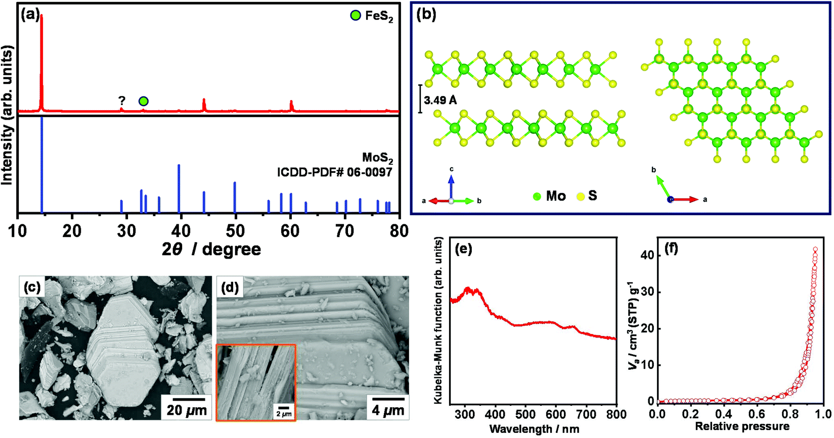 | ||
| Fig. 2 (a) XRD pattern, (b) side and top views of the crystal structure of molybdenite (2H polytype), (c and d) BSE-SEM images, (e) UV-vis DRS spectrum, and (f) N2 adsorption–desorption isotherm of molybdenite concentrate. | ||
Fig. 2e shows the UV-vis diffuse reflectance spectrum of molybdenite concentrate. As shown, molybdenite concentrate exhibits a strong light absorption in the wavelength range of 200–800 nm. An absorption edge of molybdenite concentrate is observed at approximately 435 nm, corresponding to an optical indirect band-gap energy (Eg) of 2.86 eV. Clearly, the indirect band-gap energy of molybdenite concentrate is much lower than the reported value for a bulk MoS2 crystal (Eg = 1.29 eV)21 due to their chemical and structural differences. It is known that the band-gap energy of MoS2 can easily be tuned by changing the number of layers22 and by applying a mechanical strain,23 and a direct to indirect band-gap transition is also observed. Obviously, four characteristic peaks with lower intensity at about 290–300 nm and 550–685 nm are observed in the UV-vis diffuse reflectance spectrum of molybdenite concentrate. Presumably, the peaks observed at 290–300 nm may indicate a reduction in the 2H phase of MoS2![[thin space (1/6-em)]](https://www.rsc.org/images/entities/char_2009.gif) 24,25 or the interband transition between the occupied and unoccupied orbitals,26 while the peaks noted at 550–685 nm correspond to the excitonic interband transitions at the K point of the Brillouin zone.27 It must be mentioned that the peaks representing the four excitonic electronic transitions are blue-shifted compared to those of stable dispersion of MoS2 nanosheets.26 As the specific surface area plays an important role in sensing, the specific surface area was estimated from the N2 gas adsorption–desorption isotherm shown in Fig. 2f. According to the IUPAC classification,28 the isotherm of molybdenite concentrate is type III, indicating a relatively weak adsorbent–adsorbate interactions on the surface of a nonporous or macroporous solid. The estimated specific surface area of molybdenite concentrate was 2.11 m2 g−1.
24,25 or the interband transition between the occupied and unoccupied orbitals,26 while the peaks noted at 550–685 nm correspond to the excitonic interband transitions at the K point of the Brillouin zone.27 It must be mentioned that the peaks representing the four excitonic electronic transitions are blue-shifted compared to those of stable dispersion of MoS2 nanosheets.26 As the specific surface area plays an important role in sensing, the specific surface area was estimated from the N2 gas adsorption–desorption isotherm shown in Fig. 2f. According to the IUPAC classification,28 the isotherm of molybdenite concentrate is type III, indicating a relatively weak adsorbent–adsorbate interactions on the surface of a nonporous or macroporous solid. The estimated specific surface area of molybdenite concentrate was 2.11 m2 g−1.
Various particles were observed in the BSE-SEM images of molybdenite concentrate in addition to the molybdenite-2H particles. To identify these particles, energy-dispersive X-ray spectroscopy (EDX) analysis was performed. Fig. S2 in the ESI† shows the BSE-SEM images and the corresponding EDX spectra of different particles of molybdenite concentrate. Based on the EDX data shown in Fig. S2a and S2d,† the truncated cubic and plate-like particles can be assigned to FeS2 and molybdenite-2H, respectively, and no impurities/dopants are detected, implying the high purity of both components. In Fig. S2b,† the irregular inhomogeneous particles accumulated between the truncated cubic crystals of FeS2 and plate-like particles of molybdenite-2H contain iron, copper, magnesium, aluminum, sulfur, and oxygen elements. Interestingly, the sponge-like quasi-spherical particles contain iron, magnesium, aluminum, oxygen and a small amount of sulfur (Fig. S2c†). According to the EDX data, the chemical composition of molybdenite concentrate (wt%) is 24.54 Mo, 51.41 S, 18.53 O, 3.62 Fe, 0.87 Al, 0.57 Cu, and 0.46 Mg.
The exfoliation in liquid nitrogen and dispersion in isopropanol under ultrasonication yielded a few-layer MoS2 film. As shown in Fig. S3a in the ESI,† the presence of a strong diffraction peak at 2θ = 14.3° in the XRD pattern of the exfoliated/deposited sample confirms high crystallinity of few-layer MoS2. Furthermore, Raman spectroscopy was used to estimate the thickness of the MoS2 film. For a better understanding, the Raman spectrum of few-layer MoS2 deposited on the sensing device is compared with that of bulk MoS2. As shown in Fig. S3b,† the Raman spectrum of few-layer MoS2 deposited on the sensing device shows red and blue shifts as compared to the Raman spectrum of bulk MoS2. The two vibrational modes positioned at 383.30 and 407.28 cm−1 correspond to the in-plane (E12g) and out-of-plane (A1g) phonon modes. The difference between the two modes is ∼24 cm−1 which ensures that the thickness of the deposited MoS2 film in the sensing device is about 4 nm.29,30
Molybdenite-2H collected after liquid nitrogen exfoliation was analyzed using a high-resolution analytical scanning transmission electron microscope to gain more insights into the crystal structure, and the results are shown in Fig. 3. The bright-field TEM image in Fig. 3a shows a molybdenite-2H particle with a lateral size of about 7 μm. Clearly, the main part of the molybdenite-2H particle had a darker color than its edge, suggesting that the molybdenite-2H particle is composed of several layers. No clear defects were seen in the lattice image (Fig. 3b), confirming the high crystallinity of exfoliated molybdenite-2H layers. The interplanar spacing in the lattice fringe image was found to be 0.27 nm, corresponding to the (100) atomic plane of hexagonal molybdenite-2H, which is in good agreement with the XRD data. A typical hexagonal lattice structure of molybdenite-2H was identified by indexing the SAED pattern shown in Fig. 3c. The well-ordered diffraction spots in the SAED pattern reveal the single-crystalline nature of the layered structure of molybdenite-2H. In Fig. 3d–f, the scanning transmission electron microscope (STEM) image and the corresponding elemental mapping images indicate the homogeneous distribution of Mo and S atoms (Mo:S ratio = 1.01:1.97) over the entire layered structure of molybdenite-2H.
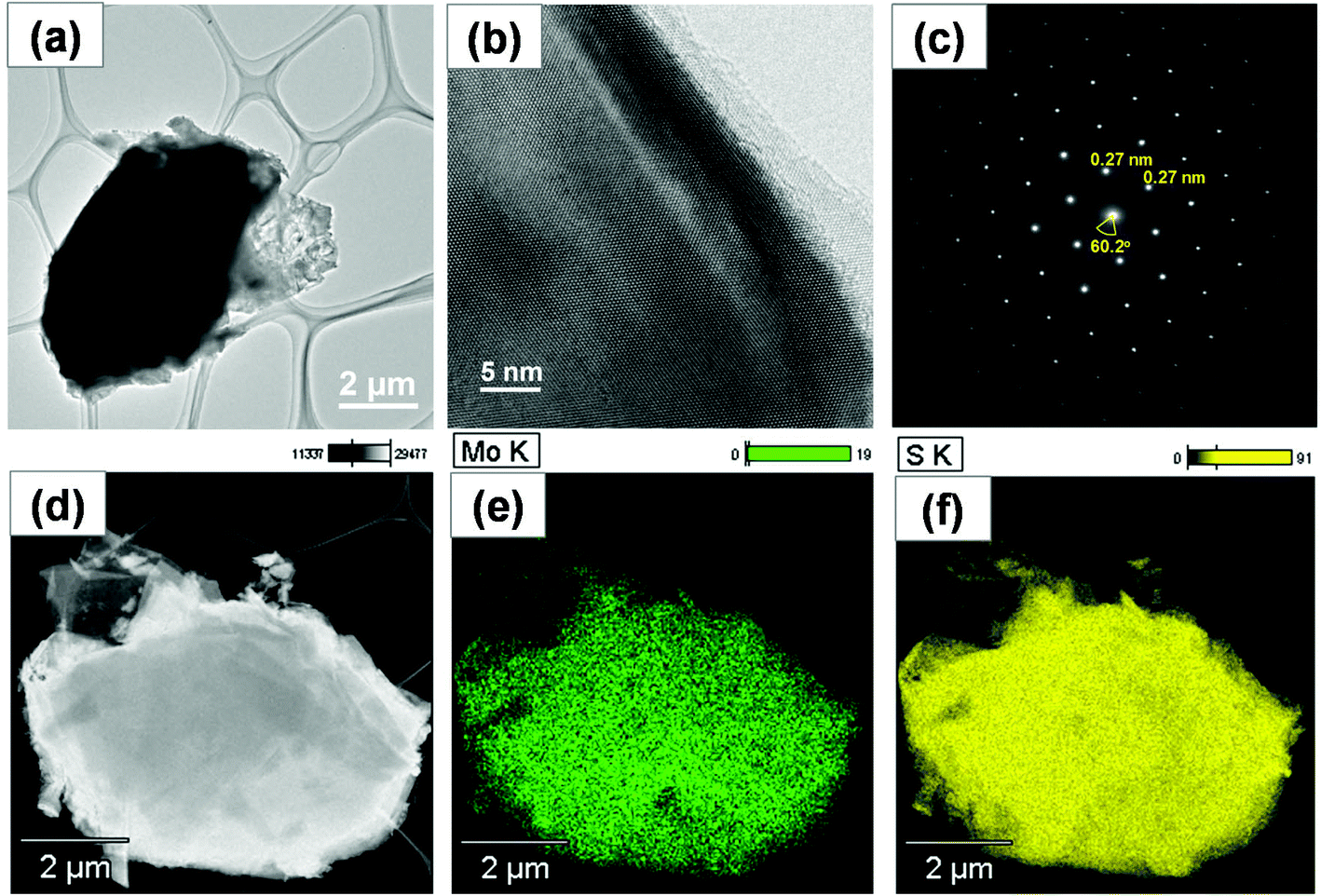 | ||
| Fig. 3 TEM (a) and HRTEM (b) images, SAED pattern (c), STEM image (d) and the corresponding EDX elemental mapping images of Mo (e) and S (f) of exfoliated molybdenite. | ||
The wide-scan XPS spectra of molybdenite concentrate before and after liquid nitrogen exfoliation are shown in Fig. 4. As shown in Fig. 4a, the XPS spectrum of molybdenite concentrate before exfoliation indicates the presence of Mo, S, O, Fe, Al, Cu, Mg and adventitious C elements. In contrast, the XPS spectrum of molybdenite concentrate after liquid nitrogen exfoliation (Fig. 4b) shows only Mo, S, and adventitious C and O elements, deducing that enriched molybdenite-2H can be produced by liquid nitrogen exfoliation. In Fig. 4c, the high-resolution XPS spectrum of Mo 3d shows the predominant Mo 3d3/2 and Mo 3d5/2 peaks at 233.0 eV and 229.9 eV, respectively, which are ascribed to the Mo4+ components of the molybdenite-2H phase. In Fig. 4d, the high-resolution XPS spectrum of S 2p are deconvoluted into two characteristic S2− components (S 2p1/2 and S 2p3/2) of the molybdenite-2H phase at 162.1 eV and 163.31 eV, respectively.31
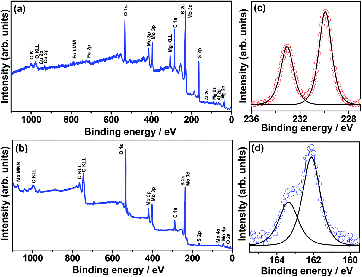 | ||
| Fig. 4 Wide-scan XPS spectra of molybdenite concentrate before (a) and after (b) liquid nitrogen exfoliation and Mo 3d (c), and S 2p (d) XPS spectra of molybdenite concentrate after liquid nitrogen exfoliation. | ||
Fig. 5 shows the XRD patterns of the molybdenite-2H films fabricated on SiO2/Si (MC1–MC3), n-type silicon (MC4 andMC5) and metallic IDC-patterned SiO2/Si (MC6) substrates. Upon increasing the speed of spin coating from 1500 rpm to 3500 rpm, the intensity of the 002 reflection in the XRD patterns of molybdenite-2H films fabricated on the SiO2/Si substrate was increased presumably due to the formation of a thicker film. A similar trend was observed for molybdenite-2H films fabricated by spin coating on the n-type silicon substrate. That is, the intensity of the 002 reflection in the XRD pattern of the molybdenite-2H film fabricated by spin coating at 1500 rpm was higher than that of the molybdenite-2H film fabricated at 500 rpm. The molybdenite-2H film fabricated by drop casting on the metallic IDC-patterned SiO2/Si substrate showed a slightly lower intensity of the 002 reflection than the other samples.
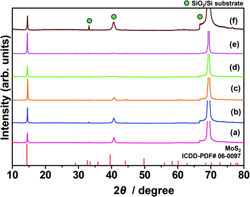 | ||
| Fig. 5 XRD patterns of (a) MC1, (b) MC2, (c) MC3, (d) MC4, (e) MC5, and (f) MC6 samples. | ||
Fig. 6 shows the SEM images of molybdenite-2H films fabricated on the SiO2/Si (MC1–MC3), n-type silicon (MC4 and MC5) and metallic IDC-patterned SiO2/Si (MC6) substrates. It can be seen in Fig. 6a that the exfoliated molybdenite-2H sheets were deposited on the SiO2/Si substrate by spin coating at 1500 rpm, and the shape of the deposited molybdenite-2H sheets was visible. However, upon increasing the spin coating speed from 1500 rpm to 3500 rpm, the deposited molybdenite-2H films became denser and less rough, and the shape of the molybdenite-2H sheets was less visible (Fig. 6b and c). Similarly, the molybdenite-2H film fabricated on the n-type silicon substrate by spin coating at 500 rpm was the least dense and rougher, showing clearly the face-to-face deposited irregular molybdenite-2H sheets (Fig. 6d). In contrast, when the spin coating speed was raised to 1500 rpm, the molybdenite-2H film became denser (Fig. 6e), indicating a close relationship between the fabricated film density and the spin coating speed. Fig. 6f shows the SEM image of the molybdenite-2H film fabricated by drop casting on the metallic IDC-patterned SiO2/Si substrate. It is clear that smaller and thinner molybdenite-2H sheets were homogeneously deposited, from which thicker molybdenite-2H sheets protruded. This indicates that spin coating is advantageous over drop casting in fabricating a homogeneous and dense molybdenite-2H film. Particularly, the MC3 sample shows a homogeneously deposited molybdenite-2H film. In Fig. S4a–c in the ESI,† the EDX spectrum and EDX elemental mapping images reveal that Mo and S are homogeneously distributed in the molybdenite-2H film, and no impurities are detected, implying high purity of the deposited film.
 | ||
| Fig. 6 SEM images of (a) MC1, (b) MC2, (c) MC3, (d) MC4, (e) MC5, and (f) MC6 samples. | ||
In recent years, MoS2 has established itself as a promising gas sensing material for detecting various environmental pollutants. It offers a higher density of states, a higher value of mobility, and a lower value of interface scattering. Late et al.32 studied the sensing performance of single- and few-layer MoS2 upon exposure to NO2 gas molecules. After comparing the results from both types of devices, it was observed that few-layer MoS2 is more suitable for sensing applications due to its excellent sensing response. The improvement in the sensing response of few-layer MoS2 is due to its different electronic structures and more stable response over time. Hence, these appealing attributes of MoS2 for gas sensing applications attract much research interest for developing highly sensitive, selective, and stable gas sensors. However, the incomplete recovery is a major bottleneck restricting the performance of MoS2-based gas sensors at lower temperatures (<100 °C).33 Therefore, a sufficient external stimulus is the stringent need for the complete recovery of practical gas sensors.
Among various available alternatives, thermal energy is one of the most widely used techniques to improve the sensing performance of the developed device. Therefore, we investigated the sensing performance of the device fabricated using the MC3 sample against different concentrations of NO2 at different temperatures (50, 100, and 120 °C). The relative dynamic response of the device was calculated as (ΔR/R0) × 100% = (Rg − R0)/R0 × 100%, where Rg is the resistance of the MC3 sample in the presence of NO2 and R0 is the base resistance of the device. As an oxidizing gas, NO2 traps electrons from the surface of the MC3 sample, resulting in the change of the charge density of the deposited film (Fig. 7a).33 The variation in the carrier concentration leads to a large increase in the resistivity of the device, and hence, a high value of sensitivity was achieved. At 50 °C, 48% and 67% sensitivities were observed upon exposure to 50 and 100 ppm NO2 gas molecules, respectively (Fig. 7b). However, the fabricated sensor was not fully recovered due to insufficient thermal energy. A strong binding energy between the MoS2 film and the NO2 molecules prevents the complete recovery of the fabricated device at 50 °C.34 Therefore, to make the fabricated device fully recoverable, the temperature of the sensor was raised to 100 °C. At this temperature, 42% and 52% sensitivities were achieved for 50 and 100 ppm NO2, respectively. Upon increasing the temperature of the device, the recovery was improved appreciably (Fig. 7c). Yet, a full recovery of the gas sensor was still not possible. Thus, the sensing behavior of the fabricated device was further evaluated at a slightly higher temperature. As expected, a full recovery of the fabricated sensor was achieved at an optimized temperature of 120 °C (Fig. 8). The fabricated device exhibited 28, 38, and 44% sensitivities to 10, 50, and 100 ppm NO2, respectively. Clearly, the sensitivity of the device increased with the increasing concentration of NO2. It was noticed that at 120 °C, the sensitivity was slightly lowered as compared to the sensitivity at 50 and 100 °C. The decrement in the sensitivity is primarily due to a higher rate of desorption than adsorption at high temperatures. Besides acceleration of the desorption process, the reduced interaction between the MoS2 surface and gas molecules at high temperature plays a crucial role in determining the sensitivity of the device. In addition, the sensing performance of the as-received molybdenite concentrate without removing the impurities was also evaluated. As shown in Fig. S5,† the sensitivity decreased from a value of ∼28% to ∼21% in the presence of 10 ppm NO2 at 120 °C. This decrement in the sensitivity is primarily due to the higher thickness of MoS2 in molybdenite concentrate and lesser availability of favorable adsorption sites for NO2. The performance of the fabricated sensing device using few-layer MoS2 was compared with earlier reports. As shown in Table S1 in the ESI,† the sensing performance of the fabricated device is consistent with the previously reported values, indicating its good sensing response.
 | ||
| Fig. 7 (a) Schematic illustration of the sensing behavior of the fabricated device based on the charge-transfer mechanism, and the sensing performance of the MC6 sample against 50 and 100 ppm NO2 at 50 °C (b) and 100 °C (c). | ||
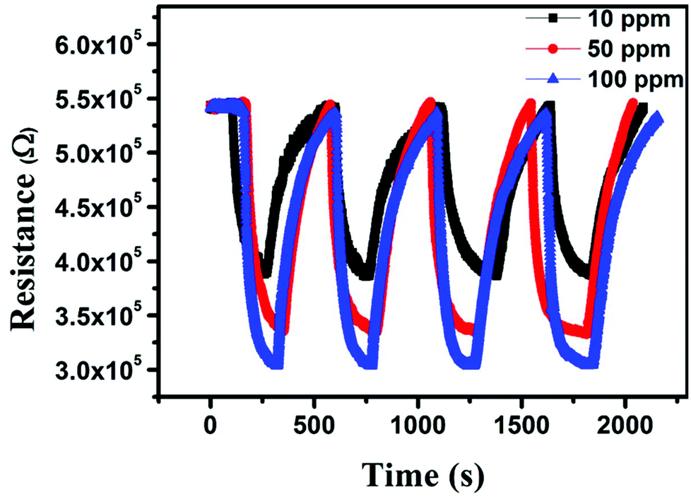 | ||
| Fig. 8 Sensing performance of the MC6 sample against NO2 gas with different concentrations at 120 °C. | ||
The adsorption of NO2 onto the predominant (002) surface of molybdenite-2H was modeled by Forcite and Adsorption Locator modules in Accelrys Materials Studio using the experimental crystallographic structural data.35 The adsorption affinities can be estimated from the distribution of field density (Fig. 9a) and the calculated differential adsorption energies (dEad/dNNO2 and (dEad/dNAr) which are the energies required for removing the sorbate of a particular component. According to the estimated differential adsorption energies, NO2 can form comparatively similar substrate–adsorbate configurations at different surfaces with a slightly preferential adsorption on the (002) surface (Fig. 9a). As the sensing behavior of the molybdenite-2H film was tested using a 5% NO2 and 95% Ar mixture, the dEad/dNi values were estimated for the adsorption of the NO2/Ar mixture onto different surfaces of molybdenite-2H:
NO 2 : −4.77 kcal mol−1 for (002) > −3.43 kcal mol−1 for (006) > −3.35 kcal mol−1 for (008)
Ar: −1.82 kcal mol−1 for (008) > −1.15 kcal mol−1 for (006) > −0.18 kcal mol−1 for (002).
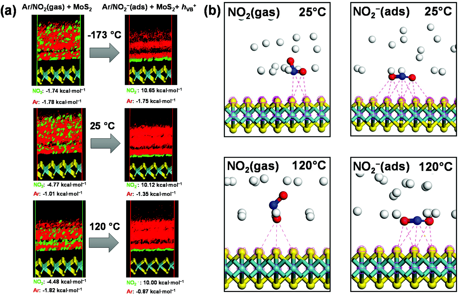 | ||
| Fig. 9 (a) Field density distribution of a 5% NO2 and 95% Ar mixture on the predominant (002) surface of molybdenite-2H. Atoms: sulphur, yellow; and molybdenum, light blue. Isosurface: NO2, green; and Ar, red. (b) Close contacts (less than 3.7 Å) of NO2/NO2− species on the predominant (002) surface of molybdenite-2H. Atoms: sulphur, yellow; molybdenum, light blue; nitrogen, dark blue; oxygen, red; and argon, grey. | ||
It is clear that NO2 in the Ar/NO2 mixture has better interaction with the surfaces of molybdenite-2H than individual NO2 (dEad/dNNO2 = 2.57 kcal mol−1).
The layered crystal structure of molybdenite-2H shows closely packed double layers with S6-coordination of Mo atom (Fig. 9). The adsorption of different adsorbate molecules like H2,36 DNA,37 CO,38 thiophene,39 and methanol40 was studied by molecular modeling on the surface of molybdenite to gain more insights into the mechanisms of catalytic reaction36,38–40 and sensing.37 It has been shown that molybdenite is a promising candidate for a new generation of gas sensors based on layered compounds. The chemical interaction mechanism for NO2 sensing was proposed as follows:41
| MoS2 + NO2(gas) = MoS2+ − NO2−(ads) | (1) |
| MoS2+ − NO2−(ads) = MoS2 − NO2−(ads) + hVB+ | (2) |
The calculation results of equilibrium adsorption of Ar/NO2(gas) and Ar/NO2−(ads) show negative values (exothermic process) of total adsorption energies at different temperatures (Table 1). Although the total adsorption energies and differential adsorption (desorption) energies dEad/dNNO2 are negative, the differential adsorption energies  are positive at different temperatures. This implies that higher temperatures should lead to the desorption of NO2 and the shift of the adsorption–desorption equilibrium to adsorption of Ar/NO2−(ads) on molybdenite-2H. The energy gain between the adsorption and desorption processes for NO2/NO2− species can be estimated as:
| Δ = dEad/dN(NO2) − dEad/dN(NO2−) ≈ 14 kcal mol−1 | (3) |
| Temperature, °C | Adsorption energy | Rigid adsorption energy | Deformation energy | dEad/dN (Ar) | dEad/dN (NO2) |
|---|---|---|---|---|---|
| MoS 2 /NO 2 (gas) | |||||
| −173 °C | −36.88 | −36.88 | 0.00 | −1.78 | −1.74 |
| 25 °C | −33.63 | −33.64 | 0.01 | −1.01 | −4.77 |
| 120 °C | −38.59 | −38.59 | 0.00 | −1.82 | −4.48 |
| MoS 2 + /NO 2 − (ads) | |||||
| −173 °C | −22.49 | −22.49 | 0.00 | −1.75 | 10.65 |
| 25 °C | −20.39 | −20.40 | 0.01 | −1.35 | 10.12 |
| 120 °C | −20.79 | −20.80 | 0.00 | −0.87 | 10.00 |
In general, the dEad/dNNO2 and  values are similar at 25 °C and 120 °C. At 120 °C, the total adsorption of Ar/NO2 (−38.59 kcal mol−1) is greater than that at lower temperatures. However, the dEad/dNNO2 value at 120 °C (−4.48 kcal mol−1) is slightly decreased when compared to the dEad/dNNO2 value at 25 °C (−4.77 kcal mol−1). The highest desorption of Ar/NO2− is observed at 25 °C (−20.39 kcal mol−1), while the desorption of NO2− at 25 °C (10.12 kcal mol−1) is similar to that at 120 °C (10.00 kcal mol−1). Thus, NO2 adsorption is still high at 120 °C with high NO2 desorption. Quantitatively, the optimal adsorption–desorption ratio of NO2/NO2− and the energy gain (−14.99 kcal mol−1) are observed at 25 °C although the largest gain in total adsorption–desorption is at 120 °C (17.80 kcal mol−1).
The calculation results show that the adsorption of Ar and NO2 molecules is impossible between the double S–Mo–S layers connected by weak van der Waals interactions. The negative and positive charges of the molybdenite-2H surface should have more influence on the electrostatic interactions between the molybdenite-2H surface and Ar/NO2− species. As a result, NO2 is adsorbed in a vertical position when compared to NO2− which is adsorbed in a horizontal position correspondingly (Fig. 9b). It is consistent with the previous data40 that the negatively charged DNA-molecules could not interact with the positively charged Mo atoms due to the stereochemical shield of the Mo atoms from the adsorption surface. Therefore, DNA could be adsorbed more effectively on the MoS2 surface via van der Waals interactions than through electrostatic interactions between the phosphate and Mo atoms. As shown in Table 1, the interaction forces between NO2− and MoS2 were analyzed, and the total interaction energy was found to be about −14 kcal mol−1. The van der Waals force is similar to the total energy, while the contribution of electrostatic interaction force is less than −1.0 kcal mol−1 in the case of NO2− adsorption. It indicates that the electrostatic interaction is relatively weak, and the main adsorption force is van der Waals interaction. This is in good agreement with our description for the molecular modeling data of close contacts between NO2/NO2− and molybdenite-2H (Fig. 9b). The number of close contacts of NO2 is less than the number of close contacts of NO2−, indicating better interaction of NO2− species with the positively charged surface of molybdenite-2H.
4. Conclusions
In summary, we have characterized molybdenite concentrate from the mining-metallurgy industry as a valuable starting material for the fabrication of an efficient and low-cost nanostructured gas sensor. After liquid nitrogen exfoliation, impurities were removed and the enriched molybdenite-2H was deposited on different substrates by spin coating and drop casting. It was found that spin coating was advantageous over drop casting in fabricating a homogeneous and dense molybdenite-2H film. The gas sensing behavior of the fabricated sensor was studied for different concentrations of NO2 at different temperatures. It was found that the temperature strongly influences the key sensing parameters of the device. The sensing behavior of the fabricated device was explained based on the charge-transfer mechanism. The molecular modeling results showed that NO2 in the Ar/NO2 mixture had better interaction with the molybdenite-2H surface than individual NO2, and the main adsorption force was the van der Waals interaction. The findings of this study reflect a straightforward approach for converting molybdenite concentrate into an efficient and low-cost nanostructured gas sensor.Conflicts of interest
There are no conflicts of interest to declare.Acknowledgements
MH would like to thank the Alexander von Humboldt (AvH) Stiftung for the research award and equipment subsidy grant (no. 3.4-8151/12 005) and The World Academy of Sciences (TWAS) for the TWAS-COMSTECH Research Grant (no. 18-455 RG/MSN/AS_C-FR3240305789). The authors wish to thank Dr. Tetsu Ohsuna of Toyota Central R&D Laboratories Inc. and Prof. Masashi Hasegawa of Nagoya University for their help with TEM observations.References
- AirNow Program of the United States Environmental Protection Agency (EPA). https://www.airnow.gov/.
- J. Cyrys, et al., Variation of NO2 and NOx concentrations between and within 36 European study areas: Results from the ESCAPE study, Atmos. Environ., 2012, 62, 374–390 CrossRef CAS.
- I. Zawadzka-Małota, Testing of mining explosives with regard to the content of carbon oxides and nitrogen oxides in their detonation products, J. Sustain. Min., 2015, 14, 173–178 CrossRef.
- T.-M. Chen, W. G. Kuschner, J. Gokhale and S. Shofer, Outdoor Air Pollution: Nitrogen Dioxide, Sulfur Dioxide, and Carbon Monoxide Health Effects, Am. J. Med. Sci., 2007, 333, 249–256 CrossRef.
- WHO Air quality guidelines for particulate matter, ozone, nitrogen dioxide and sulfur dioxide (Global update 2005, Summary of risk assessment). https://www.who.int.
- R. Kumar, N. Goel, M. Hojamberdiev and M. Kumar, Transition metal dichalcogenides-based flexible gas sensors, Sens. Actuators, A, 2020, 303, 111875 CrossRef CAS.
- R. Kumar, N. Goel and M. Kumar, High performance NO2 sensor using MoS2 nanowires network, Appl. Phys. Lett., 2018, 112, 053502 CrossRef.
- S.-Y. Cho, S. J. Kim, Y. Lee, J.-S. Kim, W.-B. Jung, H.-W. Yoo, J. Kim and H.-T. Jung, Highly Enhanced Gas Adsorption Properties in Vertically Aligned MoS2 Layers, ACS Nano, 2015, 9, 9314–9321 CrossRef.
- Y. Li, Z. Song, Y. Li, S. Chen, S. Li, Y. Li, H. Wang and Z. Wang, Hierarchical hollow MoS2 microspheres as materials for conductometric NO2 gas sensors, Sens. Actuators, B, 2019, 282, 259–267 CrossRef CAS.
- A. V. Agrawal, R. Kumar, S. Venkatesan, A. Zakhidov, G. Yang, J. Bao, M. Kumar and M. Kumar, Photoactivated mixed in-plane and edge-enriched p–type MoS2 flake-based NO2 sensor working at room temperature, ACS Sens., 2018, 3, 998–1004 CrossRef CAS.
- R. Kumar, N. Goel and M. Kumar, UV-activated MoS2 based fast and reversible NO2 sensor at room temperature, ACS Sens., 2017, 2, 1744–1752 CrossRef CAS.
- R. Kumar, N. Goel, A. V. Agrawal, R. Raliya, S. Rajamani, G. Gupta, P. Biswas, M. Kumar and M. Kumar, Boosting sensing performance of vacancy-containing vertically aligned MoS2 using rGO particles, IEEE Sens. J., 2019, 19, 10214–10220 CAS.
- H. Wang, W. Lv, J. Shi, H. Wang, D. Wang, L. Jin, J. Chao, P. A. van Aken, R. Chen and W. Huang, Efficient Liquid Nitrogen Exfoliation of MoS2 Ultrathin Nanosheets in the Pure 2H Phase, ACS Sustainable Chem. Eng., 2020, 8, 84–90 CrossRef CAS.
- W. Liu, J. Kang, W. Cao, D. Sarkar, Y. Khatami, D. Jena and K. Banerjee, High-performance few-layer-MoS2 field-effect-transistor with record low contact-resistance, IEEE International Electron Devices Meeting, 2013, pp. 19.4.1–19.4.4 Search PubMed.
- W. S. Leong, T. N. Chang and J. T. L. Thong, What does annealing do to metal–graphene contacts?, Nano Lett., 2014, 14, 3840–3847 CrossRef CAS.
- A. T. Neal, H. Liu, J. J. Gu and P. D. Ye, Metal contacts to MoS2: A two-dimensional semiconductor, 70th Device Research Conference (DRC), 2012, pp. 65–66 Search PubMed.
- H. Liu, A. T. Neal and P. D. Ye, Channel length scaling of MoS2 MOSFETs, ACS Nano, 2012, 6, 8563–8569 CrossRef CAS.
- P. F. A. Braga, A. P. Chaves, A. B. Luz and S. C. A. França, The use of dextrin in purification by flotation of molybdenite concentrates, Int. J. Miner. Process., 2014, 127, 23–27 CrossRef CAS.
- D. Yuan, K. Cadien, Q. Liu and H. Zeng, Separation of talc and molybdenite: challenges and opportunities, Miner. Eng., 2019, 143, 105923 CrossRef CAS.
- S. Castro, A. Lopez-Valdivieso and J. S. Laskowski, Review of the flotation of molybdenite. Part I: Surface properties and floatability, Int. J. Miner. Process., 2016, 148, 48–58 CrossRef CAS.
- Gmelin Handbook of Inorganic and Organometallic Chemistry, Springer-Verlag, Berlin, 8th edn, 1995, vol. B7 Search PubMed.
- K. F. Mak, C. Lee, J. Hone, J. Shan and T. F. Heinz, Atomically Thin MoS2: A New Direct-Gap Semiconductor, Phys. Rev. Lett., 2010, 105, 136805 CrossRef.
- H. J. Conley, B. Wang, J. I. Ziegler, R. F. Haglund Jr., S. T. Pantelides and K. I. Bolotin, Bandgap Engineering of Strained Monolayer and Bilayer MoS2, Nano Lett., 2013, 13, 3626–3363 CrossRef CAS.
- G. Eda, H. Yamaguchi, D. Voiry, T. Fujita, M. Chen and M. Chhowalla, Photoluminescence from Chemically Exfoliated MoS2, Nano Lett., 2011, 11, 5111–5116 CrossRef CAS.
- W. Wang, O. O. Kapitanova, P. Ilanchezhiyan, S. Xi, G. N. Panin, D. Fu and T. W. Kang, Self-assembled MoS2/rGO nanocomposites with tunable UV-IR absorption, RSC Adv., 2018, 8, 2410–2417 RSC.
- R. Ahmad, R. Srivastava, S. Yadav, D. Singh, G. Gupta, S. Chand and S. Sapra, Functionalized Molybdenum Disulfide Nanosheets for 0D–2D Hybrid Nanostructures: Photoinduced Charge Transfer and Enhanced Photoresponse, J. Phys. Chem. Lett., 2017, 8, 1729–1738 CrossRef CAS.
- Y. Yao, L. Tolentino, Z. Yang, X. Song, W. Zhang, Y. Chen and C.-p. Wong, High–Concentration Aqueous Dispersions of MoS2, Adv. Funct. Mater., 2013, 23, 3577–3583 CrossRef CAS.
- M. Thommes, K. Kaneko, A. V. Neimark, J. P. Olivier, F. Rodriguez-Reinoso, J. Rouquerol and K. S. W. Sing, Physisorption of gases, with special reference to the evaluation of surface area and pore size distribution (IUPAC technical report), Pure Appl. Chem., 2015, 87, 1051–1069 CAS.
- D.-S. Tsai, K.-K. Liu, D.-H. Lien, M.-L. Tsai, C.-F. Kang, C.-A. Lin, L.-J. Li and J.-H. He, Few-layer MoS2 with high broadband photogain and fast optical switching for use in harsh environments, ACS Nano, 2013, 7, 3905–3911 CrossRef CAS.
- C. Lee, H. Yan, L. E. Brus, T. F. Heinz, J. Hone and S. Ryu, Anomalous lattice vibrations of single-and few-layer MoS2, ACS Nano, 2010, 4, 2695–2700 CrossRef CAS.
- M. Acerce, D. Voiry and M. Chhowalla, Metallic 1 T phase MoS2 nanosheets as supercapacitor electrode materials, Nat. Nanotechnol., 2015, 10, 313–318 CrossRef CAS.
- D. J. Late, Y.-K. Huang, B. Liu, J. Acharya, S. N. Shirodkar, J. Luo, A. Yan, D. Charles, U. V. Waghmare, V. P. Dravid and C. N. R. Rao, Sensing behavior of atomically thin-layered MoS2 transistors, ACS Nano, 2013, 7, 4879–4891 CrossRef CAS.
- B. Cho, A. R. Kim, Y. Park, J. Yoon, Y.-J. Lee, S. Lee, T. J. Yoo, C. G. Kang, B. H. Lee, H. C. Ko, D.-H. Kim and M. G. Hahm, Bifunctional Sensing Characteristics of Chemical Vapor Deposition Synthesized Atomic-Layered MoS2, ACS Appl. Mater. Interfaces, 2015, 7, 2952–2959 CrossRef CAS.
- S.-Y. Cho, S. J. Kim, Y. Lee, J.-S. Kim, W.-B. Jung, H.-W. Yoo, J. Kim and H.-T. Jung, Highly Enhanced Gas Adsorption Properties in Vertically Aligned MoS2 Layers, ACS Nano, 2015, 9, 9314–9321 CrossRef.
- B. Schönfeld, J. J. Huang and S. C. Moss, Anisotropic mean–square displacements (MSD) in single–crystals of 2H– and 3R–MoS2, Acta Crystallogr., Sect. B: Struct. Sci., 1983, 39, 404–407 CrossRef.
- M. Sun, A. E. Nelson and J. Adjaye, Adsorption and dissociation of H2 and H2S on MoS2 and NiMoS catalysts, Catal. Today, 2005, 105, 36–43 CrossRef CAS.
- F. Liu, Y. Zhang, H. Wang, L. Li, W. Zhao, J.-W. Shen and L. Liang, Study on the adsorption orientation of DNA on two-dimensional MoS2 surface via molecular dynamics simulation: A vertical orientation phenomenon, Chem. Phys., 2020, 529, 110546 CrossRef CAS.
- K. Zhang, Q. Wang, B. Wang, Y. Xu, X. Ma and Z. Li, A DFT study on CO methanation over the activated basal plane from a strained two-dimensional nano-MoS2, Appl. Surf. Sci., 2019, 479, 360–367 CrossRef CAS.
- S. Li, Y. Liu, X. Feng, X. Chen and C. Yang, Insights into the reaction pathway of thiophene hydrodesulfurization over corner site of MoS2 catalyst: A density functional theory study, Mol. Catal., 2019, 463, 45–53 CrossRef CAS.
- Y. Y. Chen, M. Dong, Z. Qin, X.-D. Wen, W. Fan and J. Wang, A DFT study on the adsorption and dissociation of methanol over MoS2 surface, J. Mol. Catal. A: Chem., 2011, 338, 44–50 CAS.
- M. Donarelli, S. Prezioso, F. Perrozzi, F. Bisti, M. Nardone, L. Giancaterini, C. Cantalini and L. Ottaviano, Response to NO2 and other gases of resistive chemically exfoliated MoS2-based gas sensors, Sens. Actuators, B, 2015, 207, 602–613 CrossRef CAS.
Footnote |
| † Electronic supplementary information (ESI) available. See DOI: 10.1039/d0gc02779k |
| This journal is © The Royal Society of Chemistry 2020 |