 Open Access Article
 This Open Access Article is licensed under a
 Creative Commons Attribution 3.0 Unported Licence
Silicon photosensitisation using molecular layers†
Lefteris
Danos
 *a,
Nathan R.
Halcovitch
a,
Ben
Wood
a,
Henry
Banks
a,
Michael P.
Coogan
a,
Nicholas
Alderman
b,
Liping
Fang
c,
Branislav
Dzurnak
d and
Tom
Markvart
de
*a,
Nathan R.
Halcovitch
a,
Ben
Wood
a,
Henry
Banks
a,
Michael P.
Coogan
a,
Nicholas
Alderman
b,
Liping
Fang
c,
Branislav
Dzurnak
d and
Tom
Markvart
de
aDepartment of Chemistry, Energy Lancaster, Lancaster University, Lancaster, LA1 4YB, UK. E-mail: l.danos@lancaster.ac.uk
bDepartment of Chemistry, University of Ottawa, Ottawa, K1N 6N5, Canada
cDepartment of Electrical and Electronic Engineering, Southern University of Science and Technology, Shenzhen, Guangdong 518055, China
dCentre for Advanced Photovoltaics, Czech Technical University, 166 27 Prague, Czech Republic
eSolar Energy Laboratory, School of Engineering, Faculty of Engineering and Physical Sciences, University of Southampton, Southampton, SO17 1BJ, UK
First published on 12th November 2019
Abstract
Silicon photosensitisation via energy transfer from molecular dye layers is a promising area of research for excitonic silicon photovoltaics. We present the synthesis and photophysical characterisation of vinyl and allyl terminated Si(111) surfaces decorated with perylene molecules. The functionalised silicon surfaces together with Langmuir–Blodgett (LB) films based on perylene derivatives were studied using a wide range of steady-state and time resolved spectroscopic techniques. Fluorescence lifetime quenching experiments performed on the perylene modified monolayers revealed energy transfer efficiencies to silicon of up to 90 per cent. We present a simple model to account for the near field interaction of a dipole emitter with the silicon surface and distinguish between the ‘true’ FRET region (<5 nm) and a different process, photon tunnelling, occurring for distances between 10–50 nm. The requirements for a future ultra-thin crystalline solar cell paradigm include efficient surface passivation and keeping a close distance between the emitter dipole and the surface. These are discussed in the context of existing limitations and questions raised about the finer details of the emitter–silicon interaction.
Introduction
Silicon photovoltaics (PV) dominate the world PV market with a global share of 90% and over 500 GW accumulated worldwide PV installations, and this dominance is likely to continue.1,2 Being an indirect semiconductor, however, thick wafers are needed to ensure optimum sunlight absorption. This has an effect on the cost of production, with wafer costs comprising up to 30% of the final PV module cost.3 An attractive route to minimise the use of silicon is enhancing the excitation rate of electron–hole pairs by photosensitisation.Photosensitisation of silicon has been postulated as a method to excite silicon via energy transfer from molecules close to the surface of the silicon.4–7 This process results in the production of electron–hole pairs via non-radiative energy (rather than electron) transfer. Originally proposed by Dexter,5 the process can be thought of as a near-field dipole–dipole interaction akin to Förster resonance energy transfer (FRET), between an excited molecule and the silicon substrate in close proximity (∼0–2 nm). The result of this interaction, is the direct generation of electron–hole pairs. Since the molecular excited state is localised, the process can by-pass the momentum selection rule at the root of the indirect band gap of silicon, turning silicon effectively into a direct-gap material and reducing the amount by up to 2 orders of magnitude. Indeed, by employing a similar approach to that found in light harvesting antenna in photosynthesis, we can envisage an ultra-thin nanostructured silicon solar cell photosensitised by light harvesting units without overall efficiency loss.6,8 In this approach, the photovoltaic process is divided into two independent steps: an absorption/energy collection step carried out by the molecular light harvesting structure, and the charge generation step carried out by a thin silicon p/n junction. Each step can be optimised independently, resulting in a compact converter with minimum material requirements.
There have been experimental studies that looked at the interactions of excited states close to the surface of silicon to verify the presence of excited state energy transfer (FRET). The majority of these studies investigated the fluorescence quenching of the excited state as a function of distance to the silicon surface. A significant amount of quenching is observed as the excited state approaches closer to the silicon surface using evaporated dye layers,9–11 quantum dots,12–14 Langmuir–Blodgett (LB) monolayers,15–18 and dye loaded zeolites.19 The distance dependent data can be explained in terms of a simple damping oscillating dipole placed at a certain distance on the surface of the silicon, which is similar to fluorescence quenching near metal substrates.20–23 We discuss the physics in some detail in the modelling section. We believe that only at distances less than about 5 nm can classical FRET be observed.24 Furthermore, efficiencies in excess of the single junction Shockley–Queisser limit can be achieved, with recent advances in singlet fission25–27 and triplet–triplet annihilation.28–30
The chemical modification of Si(111) surfaces has emerged as an area of intense research activity in the past three decades7,31–33 that could provide solutions for different applications in optoelectronics.34 The Si surface chemistry of interest produces oxide free surfaces with stable monolayers of molecules that are directly bonded on the Si surface (Si–C bond). Such surfaces can be generated from hydrogen terminated Si(111) surfaces routinely produced from wet chemistry.35 A simple two-step chlorination/alkylation reaction36 can give rise to an oxide free, well passivated surface that can be further functionalised with suitable chromophores while protecting the surface from oxidation.
In this work we used a chlorination/alkylation reaction to produce three types of oxide free silicon surfaces consisting of a methylated silicon surface (Si-Me), a vinyl silicon surface (Si-Vinyl) and an allyl silicon surface (Si-Allyl) and characterised them using XPS and FT-IR. We examined their passivation properties by measuring silicon fluorescence and lifetime decay to indicate the quality of the alkyl monolayer on the silicon surface. Further functionalisation of the Si-Vinyl and Si-Allyl surfaces via a Heck coupling reaction with a perylene derivative resulted in a controlled emitter to silicon surface distance in the ‘true’ FRET regime (<2 nm). The functionalised silicon surfaces were studied with time-resolved fluorescence confocal microscopy in order to estimate the lifetime quenching of the perylene dyes. The near field region was extended in the 2–4 nm distance range with the deposition of LB monolayers of suitable perylene derivatives. We observed fluorescence quenching of up to 90% from the anchored perylene molecules for <1 nm distances, which is indicative of efficient energy transfer to silicon. We modelled our results using a modification of an earlier model for dipole emitters near metallic surfaces.21
Modelling
Dipole emission near a silicon interface
An excited molecule can lose its energy in two ways when close to an interface: radiative energy transfer and non-radiative energy transfer. In their original paper,21 Chance, Prock and Silbey (CPS) modelled the lifetime of an excited molecule near the interface between two media based on a forced damped oscillator and the complex dielectric constant of the media. The theory was able to fit and explain a series of experiments20,37 based on the LB deposition technique38 of how the lifetime of an emitter can be modified by the presence of gold, silver and copper surfaces. An excited fluorescent molecule can be modelled as an electric dipole, which can emit electromagnetic radiation not only in the far field but also in the near field. The CPS theory can be modified to model fluorescence near semiconductor surfaces instead of metals via the complex dielectric constant although it raises questions about the role of the imaginary component of the dielectric constant for a low absorbing indirect semiconductor such as silicon. In the following, we will outline the main findings of the CPS theory and how it can be modified to describe the effect of an indirect semiconductor surface on the excited state lifetime of an emitter.The interaction between the molecular dipole and silicon is characterised by the dipole–silicon distance. When the distance between the dipole and silicon is larger than the wavelength of light, the fluorescence lifetime of the dipole oscillates periodically with the variation of the dipole–silicon distance. At this distance range, the main mechanism is light interference of the far field radiation of the source wave emitted by the dipole and the reflected wave from the silicon surface.
When the dipole–silicon distance is brought closer and is less than the wavelength of light, the near field radiation of the dipole starts to couple to the trapped modes in silicon, mediated by the evanescent waves propagating along the surface. We named this process photon tunnelling,39 a process similar to quantum tunnelling through a potential barrier, which is induced by total internal reflection for our case. We estimate that for an emitter–silicon distance of 30 nm, up to 70% of emitted photons from a dye molecule are injected into the waveguide mode in silicon via tunnelling.39 This tunnelling process is especially useful when silicon is in the form of a thin film (<1 μm), for which surface texturing is not feasible.
When the distance is just a few nanometres, an electron–hole pair could be directly excited in the silicon by the proximate molecular dipole. This process is similar to Förster’s resonance energy transfer process between molecules.40
Calculation of the damping rates
For the system shown in Fig. 1, the CPS theory gives the fluorescence damping rate (inverse fluorescence lifetime) as follows: | (1) |
 | (2) |
 | (3) |
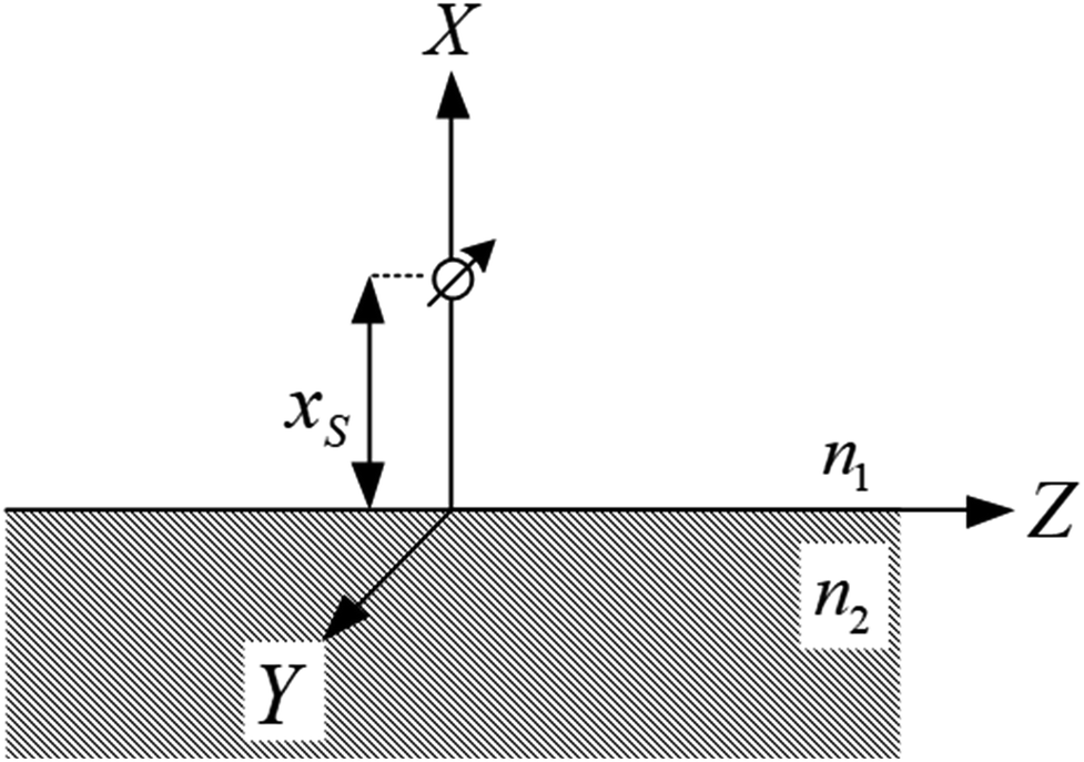 | ||
| Fig. 1 Schematic of a dipole emission near a surface used in the calculation of the fluorescence damping rates. | ||
| Far field | k p < k1 | u < 1 |
| Photon tunnelling | k 1 < kp < kSi | 1 < u < kSi/k1 |
| FRET | k p > kSi | u > kSi/k1 |
This method was first applied to dipole emission near a metal surface by Ford & Weber.41 By using this method, we arrived at the model curves plotted in Fig. 2a fitted to experimental fluorescence lifetime quenching results from a cyanine dye LB monolayer mixed with stearic acid.
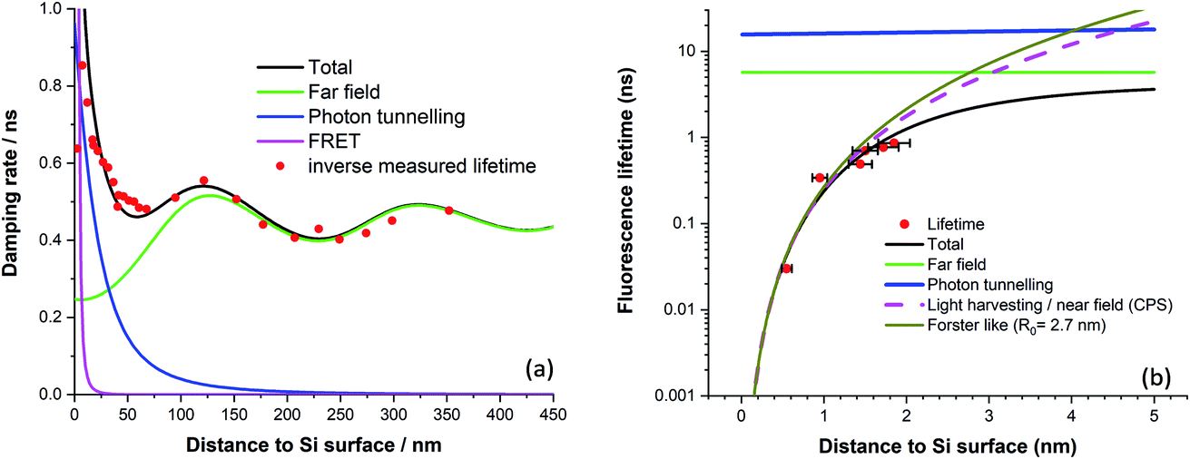 | ||
| Fig. 2 (a) Fluorescence damping rate of a mixed dye LB monolayer vs. distance to bulk silicon (after ref. 39). (b) Normalised fluorescence lifetime of various chain length diol linked protoporphyrin silicon surfaces (after ref. 24). | ||
The far field model was first given by Drexhage.37 For photon tunnelling, we did a quantum mechanical calculation for the case that silicon is in the form of a 25 nm thick waveguide,39 although evaluating the integral in the photon tunnelling region yields similar results. For the FRET region, recent results using protoporphyrin IX molecules anchored to the silicon surface demonstrate efficient energy transfer with a fit to an inverse cubic law and an estimated Förster radius of 2.7 nm, Fig. 2b.24
Experimental
Synthesis of dibromo benzoic perylene diimide (Di-Br-Pe)
Using a modified literature procedure42 a mixture of 0.5 g (1.27 mmol) of 3,4,9,10-perylene tetracarboxylic dianhydride, 0.433 g (3.18 mmol) of 4-bromoaniline, 20 g of imidazole and 0.1 g (0.456 mmol) of zinc acetate was heated at 100 °C for 2 h. The resulting mixture was further heated at 140 °C for 20 h under a nitrogen atmosphere (ESI, Fig. S1a†). The mixture was cooled to room temperature and acidified with 100 mL of 2 M hydrochloric acid with stirring for 20 minutes. The precipitate was collected by filtration and washed with copious amounts of water and methanol to remove impurities. The precipitate was finally dried under vacuum at 100 °C for 24 hours. Elemental analysis and the reaction scheme can be found in the ESI.†Synthesis of bis(n-decylimido)perylene (PTCD-C10)
To perylene-3,4,9,10-tetracarboxylic dianhydride (100 mg, 0.26 mmol) in a boiling tube, decylamine (200 μL, 157 mg, 1 mmol) was added and thoroughly mixed (ESI, Fig. S1b†). The mixture was slowly heated with a heat gun until steam began to evolve. The mixture was heated, maintaining a steady evolution of gas, until the resulting red/brown residue became viscous. Following cooling, the boiling tube was broken open and the residue was extracted repeatedly into boiling chloroform. The combined chloroform extracts were filtered to remove broken glass and then concentrated under vacuum to around 10 mL and the product was collected by filtration to give a red powder (104 mg, 0.16 mmol, 59%). Elemental and NMR analysis can be found in the ESI.†Synthesis of functionalised silicon surfaces
All solvents used in the silicon surface chemistry were anhydrous, stored in a glove box under nitrogen and used as received from Merck. The silicon substrates (10 × 10 mm squares, float zone, n-type, 25 Ω cm−1, 500 μm thickness) were polished on both sides and cleaned in Decon 90, acetone, and isopropanol followed by exposure to UV light in a UV Ozone system on each side for 20 min at 60 °C. They were then placed in a solution of hydrogen peroxide in sulfuric acid (1![[thin space (1/6-em)]](https://www.rsc.org/images/entities/char_2009.gif) :3, 45 minutes), followed by a thorough rinse in ultra-pure water. The surface of the silicon was etched in semiconductor grade ammonium fluoride (degassed, 15 minutes) to remove the native oxide layer and hydrogen-terminate the surface. After drying under flowing nitrogen, the sample was passed into a nitrogen-filled glovebox using a vacuum desiccator for further functionalisation.
:3, 45 minutes), followed by a thorough rinse in ultra-pure water. The surface of the silicon was etched in semiconductor grade ammonium fluoride (degassed, 15 minutes) to remove the native oxide layer and hydrogen-terminate the surface. After drying under flowing nitrogen, the sample was passed into a nitrogen-filled glovebox using a vacuum desiccator for further functionalisation.
The hydrogen-terminated silicon surfaces were immersed in a saturated solution of phosphorus pentachloride in chlorobenzene (110 °C, 2 hours) to which a few grains (<1 mg) of benzyl peroxide were added as a radical initiator. The sample was then washed in chlorobenzene followed by tetrahydrofuran (THF) and immersed in a 1.0–1.6 M Grignard solution of XMgCl (where X = methyl, vinyl and allyl groups) in THF (110 °C, 24 hours). After washing in THF and sonication in methanol, the samples were ready for further spectroscopic characterisation.
The vinyl (“Si-Vinyl”) and allyl (“Si-Allyl”) terminated Si(111) surfaces were washed in THF and acetonitrile, and immersed in a solution of dibromoperylene in 1:10 triethylamine:acetonitrile (Di-Br-Pe) (15 mL total) for a Heck coupling reaction.43,44 To this, palladium acetate (<0.01 g) was added and the resulting solution was heated to 100 °C for 24 hours in a pressure vessel. The functionalised silicon surfaces were removed from the glovebox, and sonicated in acetonitrile (10 × 5 mL, 5 minutes per cycle) followed by methanol (2 × 5 mL, 5 minutes per cycle). The resulting perylene functionalised surfaces (“Si-Vinyl-Pe” and “Si-Allyl-Pe”) were further washed with isopropanol and a lens tissue was dragged across the surface to ensure no physisorbed perylene moieties were left behind. After drying under nitrogen, the samples were characterised using spectroscopy.
Langmuir–Blodgett (LB) films
Substrates (quartz slides and silicon) were first washed in a warm solution of Decon 90 detergent, using abrasion to clean the surfaces. The slides were then sequentially sonicated in Decon 90, deionised water and ethanol. The slides were then dried and exposed to UV light in a UV Ozone system for 30 minutes, followed by exposure to piranha solution (3 parts H2SO4 to one part H2O2) for at least 30 min. The samples were exposed to propanol vapours to dry the surface and a final stream of nitrogen to remove any dust for further investigation. Once the slides had been cleaned, they were then exposed to hexamethydisilazane vapours (HMDS) overnight in a lidded glass staining jar to give good hydrophobic adhesion to the surface of the glass.Stock solutions in chloroform of pure perylene dye (PTCD-C10)45 and stearic acid (SA) were made up to concentrations of 1 mg per ml. Stock solutions of 10−4 M were prepared for mixtures of PTCD-C10 and SA with 1:1, 1:10, 1:25, 1:50 and 1:1000 molar ratios for the deposition of the mixed monolayers. Monolayer and multilayer LB films were fabricated using a Nima Trough (Nima Technology, UK) equipped with three dipping wells and barriers. Millipore ultrapure water was used with a resistivity > 18.2 Mohm and a pH of 6–7. Mixed chloroform solutions were deposited in 10–25 μl aliquots onto the surface of the water in the trough, depending on the amount of material needed, and were left for 15 minutes to allow the chloroform to evaporate. Three compressions were performed before any deposition in order to allow the film to anneal. All monolayers were deposited at a constant pressure of 26 mN m−1. A schematic of each sample structure is shown in Fig. S3, in the ESI.†
Absorption steady state spectra
Absorption spectra were measured using a UV-Vis absorption spectrometer (Cary 60, Agilent) in the spectral range 300–800 nm. For all fluorescence measurements in solution (chloroform) we ensured the maximum absorption peak was always less than A < 0.1 in order to avoid any re-absorption effects.Emission steady state spectra
Emission spectra were measured with a time-resolved fluorescence spectrometer (FluoTime 300, PicoQuant). The sample was excited with a 480 nm pulsed diode laser (LDH-P-C-485, PicoQuant) operated at 40 MHz. The emission spectrum was recorded at right angles to the excitation beam with a Peltier cooled photomultiplier (PMA-C 192-M, PicoQuant) in the spectral range of 560–850 nm and with a bandwidth of 5 nm. A 488 nm band edge filter (Semrock) was used to block unwanted laser scattering. Signals were digitised with a Time Harp 260 PCI card (PicoQuant) operated in steady state mode. Normalised absorption and emission spectra and decay curves from PTCD-C10 and Di-Br-Pe in solution are shown in Fig. S4, in the ESI.†Silicon fluorescence emission and decays
Silicon emission spectra and decay curves were recorded at right angles to the excitation laser beam from different functionalised surfaces using a fluorescence spectrometer (PicoQuant, FT300) equipped with a thermoelectric cooled NIR-PMT unit (Hamamatsu, H10330A-45) with a spectral range of 950 nm to 1400 nm. The samples were excited with a 730 nm picosecond pulsed diode laser (P-C-730, PicoQuant) with 40 MHz repetition rate. Signals were digitised with a Time Harp 260 PCI card (PicoQuant). Decay curves were obtained at the maximum of the emission (1135 nm or 1200 nm) with bursts of multiple pulses in order to improve the signal sensitivity. This enabled the recovery of a high signal for the long lifetime samples. The time resolved decay curves were analysed using FLUOFIT software (PicoQuant) using a two-exponential model.Time resolved emission spectra (TRES) and fluorescence decays
Time resolved emission spectra (TRES) and fluorescence decays from mixed perylene dye LB monolayers were measured using time correlated single photon counting (TCSPC) with a fluorescence spectrometer (PicoQuant, FT200 or FT300) equipped with a photomultiplier (PMA-185 or PMA-C 192-M, PicoQuant). The samples were excited with either 440 nm (LDH-P-C-440B, PicoQuant) or 480 nm (LDH-D-C-485, PicoQuant) picosecond pulsed diode lasers operated at a 40 MHz repletion rate and with a 200 ps full width half maximum (FWHM) instrument response function (IRF). The emission signals were digitised using a high-resolution TCSPC module (PicoHarp 300, PicoQuant) with 4 ps time width per channel. The emission from the LB monolayers on glass and silicon substrates were collected at right angles to the excitation laser beam and the emission arm was fitted with a 440 nm (Chroma) or 488 mm (Semrock) edge pass filter before the monochromator with a 8 nm or 5 nm spectral bandwidth.Fluorescence lifetime imaging microscopy (FLIM)
Fluorescence lifetime measurements were performed on the organic monolayers on glass and silicon substrates with an inverse fluorescence lifetime microscope (MT200, PicoQuant). The body of the microscope consisted of a modified Olympus IX73 equipped with a 100× air lens objective with numerical aperture (NA) of 0.90 (MPlanFL N, Olympus). The MT200 system was configured with an objective scanning using a piezo XY stage (PI-721.CDQ) where the objective is moved instead of the sample. The samples were excited using a 485 nm pulsed diode laser (LDH-P-C-485, PicoQuant) operated at 10 or 20 MHz with an optical power between 0.1–0.25 μW. The emitted fluorescence was spectrally cleaned with a dichroic mirror and a transmission band edge filter (510 nm) or a transmission band pass filter (600–660 nm). A pinhole of 75 μm was employed to reject light that was out of focus. The fluorescence was detected using single photon counting with an avalanche diode (SPAD-100, PicoQuant) and digitised with a Time Harp 260 PCI card (PicoQuant). The IRF had a FWHM resolution of 250 ps and 24 ps per channel time increment. Image scans were performed over an area of 80 × 80 μm2 with a varied pixel composition ranging from 256 × 256 pixels up to 640 × 640 pixels. The overall amount of photons per image was used as the measured decay curve. Lifetime image analysis was not suitable for the Si-Vinyl-Pe and Si-Allyl-Pe samples because of low photon counts detected per pixel but FLIM analysis was possible for the LB perylene mixed monolayer deposited on glass because of higher photon count rates. All decay curves were analysed using multi-exponential models via an iterative reconvolution process using SymPhoTime software (PicoQuant). Fit quality was assessed from the χ2 parameter and weighted residuals. An example of a FLIM image and decay curve for a mixed (PTCD-C10:SA) monolayer deposited on glass with SA in a 1:25 molar ratio is shown in Fig. S7, in the ESI.†
Variable angle spectroscopic ellipsometry (VASE)
The thickness of the organic monolayer was measured over a spectral range of 200 nm to 1000 nm at three different incidence angles (60°, 65°, and 70°) using a spectroscopic phase modulated ellipsometer (M-2000 V Automated Angle, J. A. Woollam Co., Inc., USA). The data collected were analysed using a three-layer model (substrate/monolayer/air) using silicon for the substrate and a Cauchy model for the monolayer. Multiple readings were taken from each sample and averaged over all consistent measurements. Examples of model fits for a mixed perylene monolayer with stearic acid deposited on silicon are shown in Fig. S8.†Infrared absorption spectra
All IR spectra were collected using a Shimadzu IRTracer-100 equipped with a deuterated lanthanum α alanine doped triglycine sulfate (DLATGS) detector or a mercury cadmium telluride (MCT) detector. Spectra were collected with the Shimadzu software package between 500 and 4000 cm−1 at a resolution of 4 cm−1. The spectra were collected either in a transmitted geometry or using a variable angle specular reflectance accessory (Pike, VeeMax III) equipped with an infrared polariser (p-polarised) at an incidence angle of 60 degrees with the surface. Background scans of a native oxide, hydrogen terminated or chlorine terminated silicon surface were used to record the absorption spectra. Spectra were collected as the sum of 512 scans and an applied atmosphere background to remove peaks due to parasitic absorption of CO2 and H2O .X-ray photoelectron spectroscopy (XPS)
XPS measurements were performed in triplicate on the samples using a Thermo Scientific K-Alpha spectrometer for a survey scan and with the Si 2p and C 1s regions investigated in detail. The Si-Cl, Si-Me, Si-Vinyl and Si-Vinyl-Pe samples were sent for XPS measurements at the Nexus national EPSRC XPS users service at Newcastle University.The Si 2p (96–100 eV) and C 1s (280–297 eV) bonding regions were investigated in detail to reveal the bonding of the monolayer to the silicon surface. Spectra were fitted to a Shirley background and were subtracted. Deconvolution of the spectra was performed by fitting multiple Gaussian bands until the residual standard deviation reached a minimum using peak fitting software (CasaXPS). The position of the Si 2p(3/2) peak was found to be approximately 0.6 eV lower than that of the Si 2p(1/2) peak and double the integrated peak area. Three Gaussian functions were used to fit the peaks for the Si–C bond at 284.0 eV, C–C bond at 285.0 eV, and C–O or C![[double bond, length as m-dash]](https://www.rsc.org/images/entities/char_e001.gif) O bonds at 286.0 eV, although the peak centres slightly changed.46 We report surface coverages of the vinyl terminated Si(111) surfaces relative to the methyl terminated Si(111) surfaces by comparing the areas of the Si–C bond peaks to the Si 2p peak for the same sample.47
O bonds at 286.0 eV, although the peak centres slightly changed.46 We report surface coverages of the vinyl terminated Si(111) surfaces relative to the methyl terminated Si(111) surfaces by comparing the areas of the Si–C bond peaks to the Si 2p peak for the same sample.47
Results and discussion
The different functionalised Si(111) surfaces prepared in this study are shown in Scheme 1. The methyl, vinyl and allyl Si(111) terminated surfaces were prepared using a modified chlorination/alkylation reaction that is known to produce well-passivated Si surfaces with good coverages.48–50 The successful attachment of the molecular chains was confirmed using polarised infrared (IR) absorption (Fig. S9, in the ESI†) and X-ray photoelectron spectroscopy (XPS) measurements (Fig. S10, in the ESI†). A section of the IR spectra for the Si-Vinyl and Si-Allyl surfaces shows C–H stretches in agreement with previous studies (Fig. 3a and b).50 XPS confirmed that the vinyl group was attached on the silicon surface in the C 1s region and showed no silicon–oxygen peaks in the Si 2p region, confirming that an oxide free surface was prepared (Fig. 3c and d). Molecular coverage for the vinyl terminated surfaces was estimated to be 95% ± 5% by comparing the ratio of the XPS C–Si/Si 2p for the vinyl terminated surface to the methyl terminated surface.49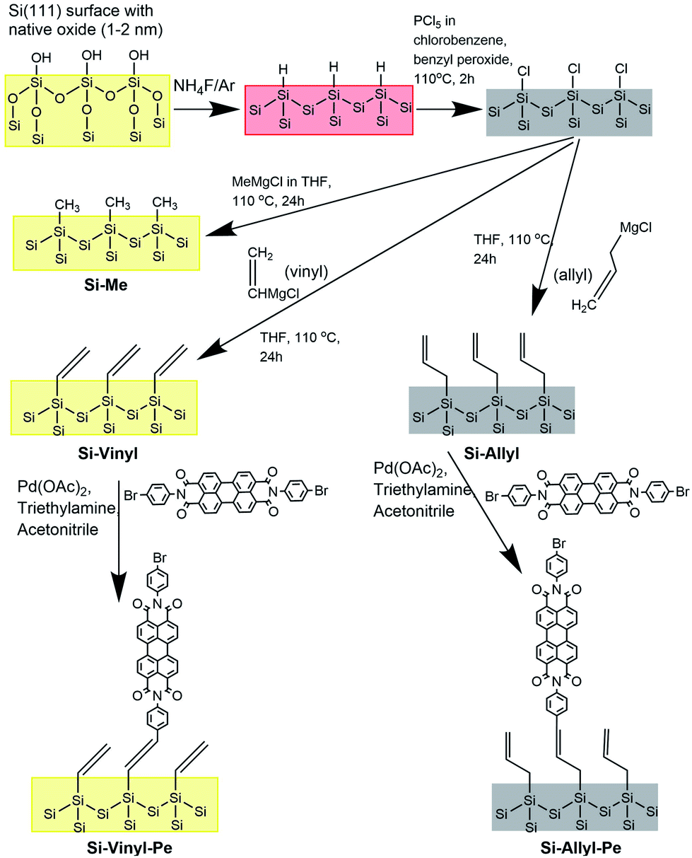 | ||
| Scheme 1 Reaction scheme for the synthesis of the alkylated/perylene silicon surfaces. | ||
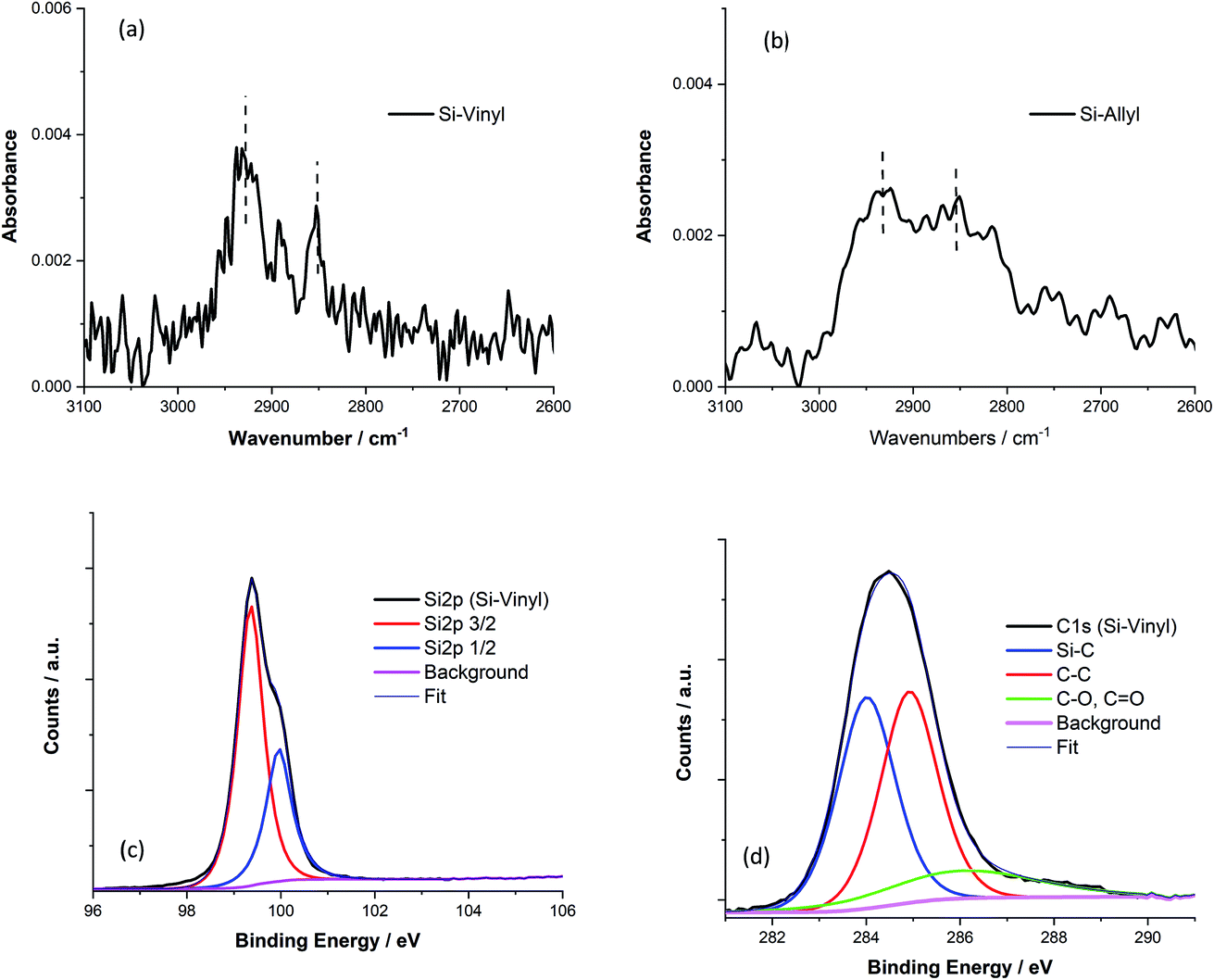 | ||
| Fig. 3 (a) Polarised reflection IR spectrum of the C–H stretching region for the Si(111)-Vinyl surface. Peaks at 2920 cm−1 and 2985 cm−1 are indicated on the spectrum and correspond to the C–H asymmetric and symmetric stretching modes respectively. (b) Polarised reflection IR spectrum of the C–H stretching region for the Si(111)-Allyl surface. Peaks at 2920 cm−1 and 2850 cm−1 are indicated on the spectrum and correspond to the C–H asymmetric and symmetric stretching modes respectively of (CH2). (c) High resolution XPS spectra of the Si 2p region for the Si(111)-Vinyl surface showing Si 2p3/2 (red) and Si 2p1/2 (blue). (d) High resolution XPS spectra of the C 1s region for the vinyl terminated Si(111) surface showing C–Si (blue), C–C (red), and C–O (green). | ||
Passivation using alkyl layers
The alkylation of silicon surfaces has proven to provide excellent passivation properties using low-temperature surface modifications.48,49 Surface photovoltage (SPV) measurements on methyl terminated Si(111) surfaces have revealed unusually large SPV signals that can only be explained by charge accumulation in the Si(111) interface during the alkylation procedure.47–52 Similar surface chemistry treatments have resulted in a p/n junction near the surface of silicon.53The passivation properties of the methyl, vinyl and allyl terminated silicon surfaces were investigated by measuring the silicon emission spectra and decay curves (Fig. 4). There is a visible difference in the spectral shape of the Si emission peak (λmax = 1133 nm, and FWHM = 100 nm) between the methyl, vinyl and allyl Si(111) surfaces and chlorine terminated (λmax = 1200 nm, and FWHM = 230 nm) Si(111) which is similar in shape with the Si emission peak from a clean Si(111) surface with the native oxide present (Fig. 4a). The observed difference in the emission peak shape is attributed to the improved surface passivation of the alkylated Si(111) surfaces and the elimination of surface traps. In contrast, the broad Si emission peak observed for the chlorine terminated Si surface (and for the native oxide) indicates poor surface passivation which is consistent with previous work.47,50
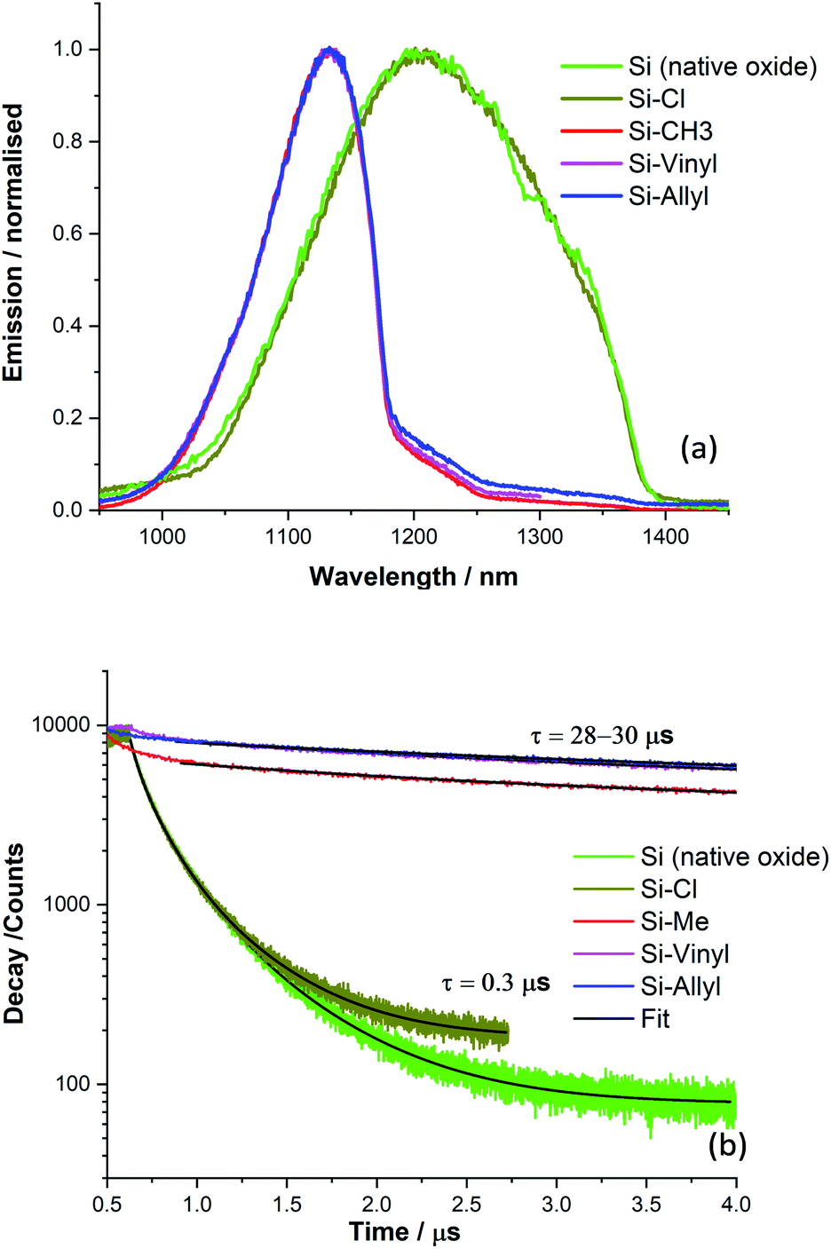 | ||
| Fig. 4 (a) Emission spectra of various silicon treated surfaces; a clean silicon surface with native oxide present, Si (native oxide), a chlorinated silicon surface (Si-Cl), a methyl terminated silicon surface (Si-Me), a vinyl terminated silicon surface (Si-Vinyl) and an allyl terminated silicon surface (Si-Allyl). (b) Emission decay curves from the functionalised silicon surfaces at the maximum emission. | ||
The passivation properties of the Si-Me, Si-Vinyl and Si-Allyl surfaces were further investigated by measuring the silicon fluorescence decay curves (Fig. 4b) and this revealed an effective recombination lifetime two orders of magnitude higher than those of the native oxide and chlorinated surfaces, indicating significant improved passivation. The very fast decay observed for the Si-Cl and Si (native oxide) samples is indicative of the presence of several surface traps.
Transient photoluminescence using single photon counting has been used to separate the surface and bulk recombination in silicon.54 In this case, we applied a simple model and the measured effective recombination lifetime was converted to the surface recombination velocity (SRV) of electron–hole pairs assuming (guaranteed from the wafer) a high silicon bulk lifetime (>1000 μs).48,49,51 For the double-sided polished surfaces, we estimated a surface recombination velocity of 830 cm s−1. Similar and even better SRV values were obtained using covalently attached monolayers and showed as good passivation properties as those obtained using traditional passivation techniques. In this case, vinyl monolayers can be used for effective silicon surface passivation.
Attachment of perylene
The Heck coupling reaction was used, as this reaction has been shown to work for bromine and chlorine-halogenated chromophores, and is a low temperature process widely investigated in the literature.43,44 Only trace amounts of the metal catalyst are required, making this a very attractive method for future scale-up (Scheme 1). The structures of the vinyl and allyl terminated surfaces resulting from the attachment of Di-Br-Pe are shown in Fig. S2 (ESI†).The successful attachment of the perylene dye was confirmed by XPS and FT-IR. The integrated area ratio of the XPS N 1s bond peak relative to the Si–C/Si 2p XPS peak for the Si-Vinyl-Pe sample gave a 5% coverage accounting for the presence of two nitrogen atoms in the perylene derivative (Fig. S10e, ESI†). The carbon C 1s bond peak also indicated that CO was present on the monolayer which can be attributed to the perylene molecules (Fig. S10d, ESI†). A large amount of Pd 3d was observed for the Si-Vinyl-Pe samples in the XPS spectrum. Furthermore, recombination lifetime measurements performed on a similar surface with a cyanine dye attached to a vinyl terminated surface coupled via the Heck reaction indicated a significant decrease in the recombination lifetime.55 The recombination lifetime did not change after multiple washes, confirming that the metal contamination could not be removed by washing. A reason for this could be the incorporation of palladium on the silicon surface leading to heavy metal contamination and a dramatic reduction in the electron–hole recombination lifetimes. A repeated procedure using a longer alkene linker (1-decene) in order to move the palladium catalysis further from the surface produced similar reduced recombination lifetimes. The Heck reaction might be disadvantageous for the functionalisation of alkene terminated silicon surfaces for photosensitised solar cells and a catalyst free approach might be more suitable.56
LB monolayers of perylene
In previous work, we studied the energy transfer of an excited molecule to silicon using LB monolayers of mixed carbocyanine dyes with stearic acid.16–18,39 Fluorescence lifetime quenching results were obtained for distances greater than 2 nm of the emitter to the surface of the silicon since the native oxide present in the silicon was not removed. The preparation of inert spacer structures can be achieved using stearic acid (SA) for distances up to 30 nm or thermal oxide for greater distances from the silicon surface. Accurate determination of the spacer thickness can be determined using spectroscopic ellipsometry.In this study, we used a 10 carbon long chain modified perylene tetracarboxylic derivative (PTCD-C10) as a monolayer material to deposit LB films on glass and silicon substrates at different molar mixing ratios with stearic acid (SA) (Fig. S3, in the ESI†).
The fluorescence emission in dilute solutions from both perylene derivative molecules (PTCD-C10 and Di-Br-Pe) used in this study showed the expected three peak vibronic structure at 534 nm, 575 nm and 625 nm with a slight 2 nm blue shift observed for the emission peaks of Di-Br-Pe (Fig. S4a, in the ESI†). The emission spectra are essentially mirror images of their respective absorption spectra (Fig. S4b, in the ESI†). The solution fluorescence decays show the expected mono-exponential lifetime with excited state lifetimes τ(Di-Br-Pe) = 3.7 ns and τ(PTCD-C10) = 4.0 ns (Fig. S4c and d, in the ESI†).
In condensed phases such as the LB monolayers, concentration quenching occurs with the appearance of a red-shifted emission band due to excimer formation (Fig. S5a, in the ESI†).57 The decay lifetimes were multi-exponential and the average lifetimes remained essentially the same irrespective of the mixing ratio with SA because the PTCD-C10 molecules pack close together forming aggregates on the water surface. Time resolved emission spectra (TRES) showed the absence of any monomers in the monolayer and emission occurred from aggregates and excimer formation in the monolayer. The excimer emission spectrum observed from different mixed perylene monolayers is broad with a peak between 650 and 670 nm depending on the concentration of perylene molecules in the monolayer (Fig. S6a–c, in the ESI†). Only at a very low PTCD-C10 concentration in the monolayer with SA (1:1000) does the PTCD-C10 lifetime approach the one observed for dilute solutions.
The measured emission and decay curves from the PTCD-C10 mixed monolayer (1:25) on glass were used as the true ‘unquenched’ data in order to normalise all measurements taken from the PTCD-C10 monolayers on silicon substrates (Fig. S7b, in the ESI†). PTCD-C10 monolayers were deposited on silicon in two different configurations (Pe-LB1 in a hydrophilic Si prepared surface and Pe-LB2 in a hydrophobic Si prepared surface), giving rise to emitter distances ranging from 2–4 nm (Fig. S3, in the ESI†). Spectroscopic ellipsometry was used to measure the distance to the surface of the silicon (Fig. S8, in the ESI†).
FLIM measurements and fit to the FRET region
Fluorescence lifetimes were measured using time-resolved fluorescence confocal microscopy. The overall decay intensities were analysed for each image with several image measurements taken from different regions and lifetimes were averaged. Because of the low photon count rate per pixel, a direct analysis of the lifetime images (FLIM) was not possible for Si-Vinyl-Pe and Si-Allyl-Pe samples. Selected fluorescence lifetime images are shown in Fig. 5. The functionalised Si(111) surfaces (Fig. 5a and b) show the perylene molecules distributed across the surface. Formation of aggregates on the surface is possible due to the presence of the large pi-ring of the perylene molecule. The dark areas correspond to regions of the Si(111) surface that were not functionalised with the perylene molecules. The same pattern was observed for each perylene functionalised silicon surface studied. The LB monolayers deposited on silicon from the PTCD-C10 perylene derivatives mixed with SA showed different patterns (Fig. 5c and d). The strong intermolecular interactions of the perylene molecules on the surface of water in a Langmuir monolayer resulted in the molecules forming ‘fibre like’ structures on the deposited LB monolayers on the glass and silicon substrates. The dark areas observed in the FLIM images are due to the presence of stearic acid in the mixed PTCD-C10:SA (1:25) monolayer. It is evident that the PTCD-C10 molecules pack closely together on the surface of water, forming aggregates irrespective of the SA mixing ratio. Only at high mixing ratios with SA greater than 1:1000 were we able to observe isolated PTCD-C10 molecules on the LB monolayer.
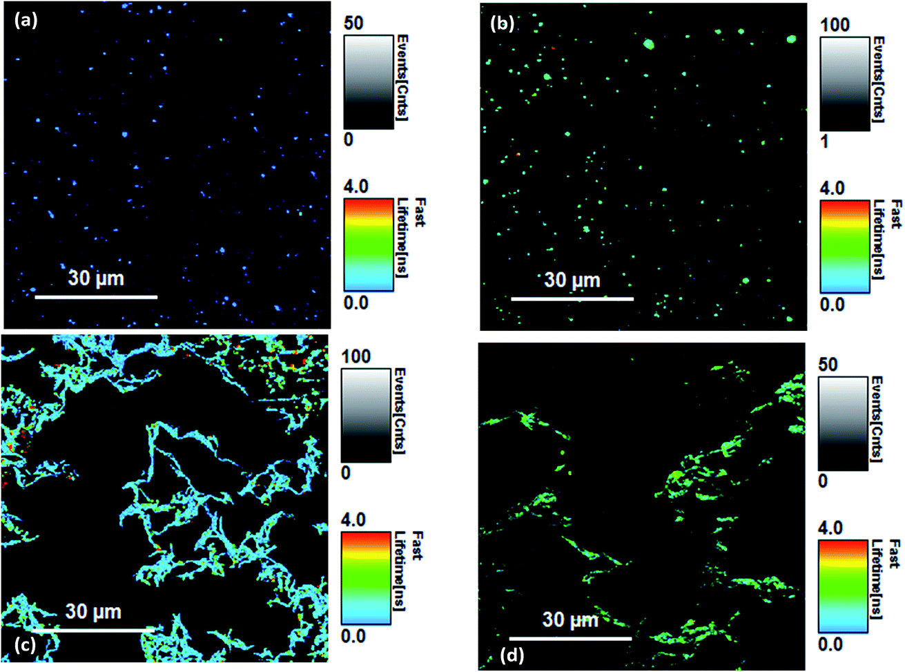 | ||
| Fig. 5 Fluorescence lifetime imaging (FLIM) scans of (a) the Si-Vinyl-Pe surface, (b) the Si-Allyl-Pe surface, (c) the Pe-LB1 Si surface and (d) the Pe-LB2 Si surfaces. | ||
The overall decay curves obtained for each sample are shown in Fig. 6a together with decay fits. There is significant fluorescence quenching in the lifetimes observed for the functionalised Si(111) surfaces (Si-Vinyl-Pe, and Si-Allyl-Pe) and the LB monolayer (PTCD-C10:SA) samples with respect to the ‘unquenched’ decay curves. In fact, over 90% quenching is observed for the fluorescence lifetime of Si-Vinyl-Pe, indicating efficient FRET from the perylene molecules to silicon. The fluorescence lifetimes measured for the samples prepared in this study are plotted in Fig. 6b as a function of the emitter–silicon distance in the near field regime (0.5–5 nm). We have modelled the observed fluorescence lifetime quenching with a modified CPS theory with input parameters: the refractive index of the silicon substrate at the maximum emission wavelength (λ = 650 nm), the refractive index of the capping layer, the fluorescence quantum yield, and the ‘true’ unquenched lifetime of the emitter. We have used an isotropic transition dipole orientation for the perylene molecules but a vertical and horizontal configuration gives similar model curves for such close distances to the surface of the silicon (Fig. S11, in the ESI†). We can also describe our results with a Förster-like energy transfer between the perylene molecules and the silicon with an inverse cubic dependence giving rise to an estimate Förster radius, R0 = 2.5 nm.
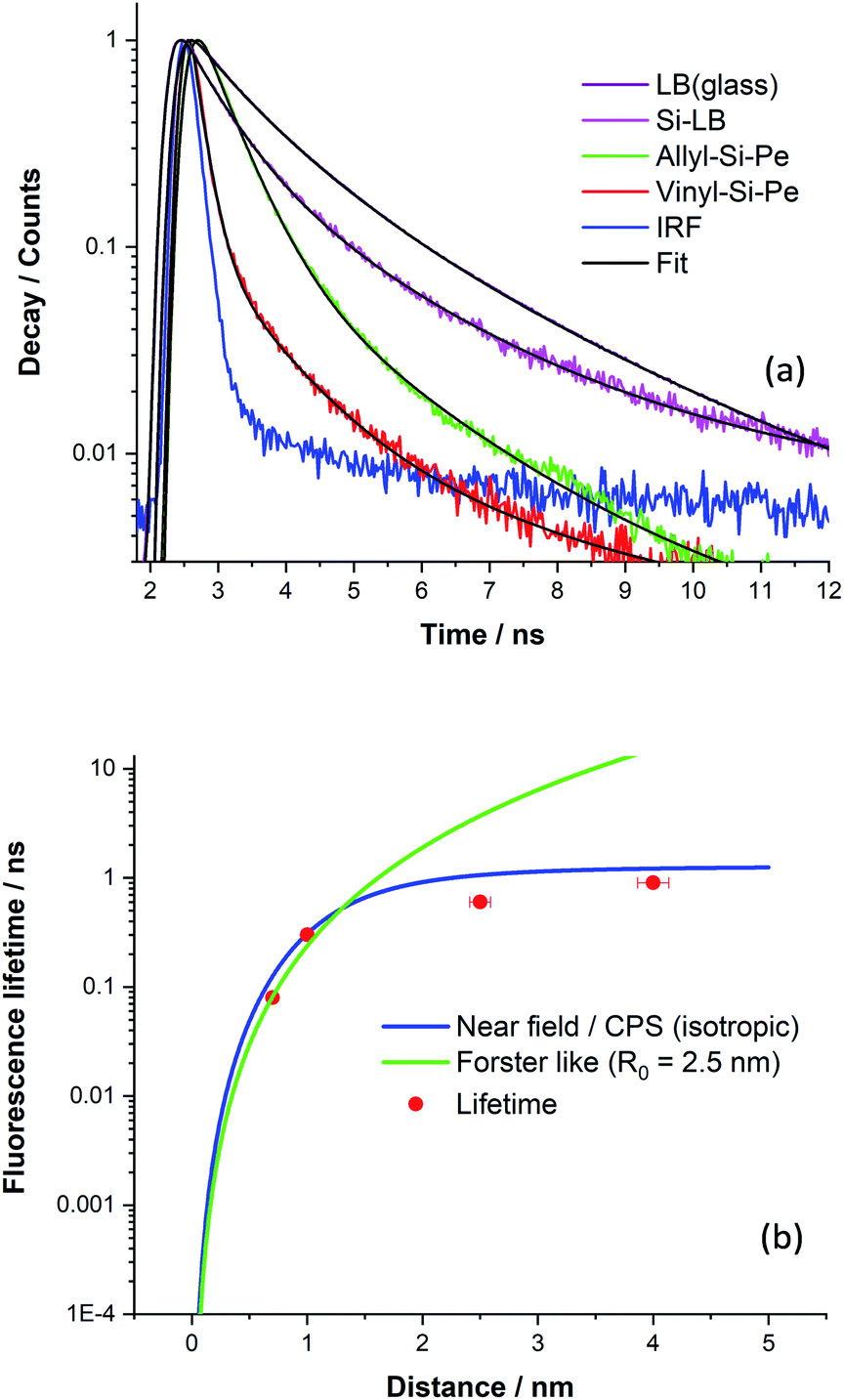 | ||
| Fig. 6 (a) Normalised fluorescence decay curves for different perylene surfaces. (b) The experimental fluorescence lifetimes of different perylene functionalised surfaces fitted to Chance–Prock–Silbey (CPS, full blue line) and to an inverse cubic (Förster) fit. | ||
The CPS model adequately describes the observed lifetime data but there is room for improvement. In particular, the fluorescence quantum yield input parameter for the emitter was set to be low (q ∼ 0.1) in order to achieve a good fit. This might be true because of the presence of aggregates in the PTCD-C10 monolayer and perhaps for the perylene attachment on the silicon as revealed by the FLIM measurements. The other input parameter is the true unquenched lifetime, which for the PTCD-C10 LB monolayer, was estimated from the fluorescence lifetime on glass (τ = 1.3 ns). But for the Si-Vinyl-Pe and Si-Allyl-Pe samples, we expect this to be higher for isolated molecules anchored on the surface of glass, approaching the one observed in solution (τ = 3.7 ns). Despite the limitations of the model, the observed fluorescence quenching is described well by the fitted model in the near field ‘true’ FRET region which takes place for emitter–silicon distances up to 5 nm. The estimation of the Förster radius for the FRET observed between the perylene molecules and the silicon gives similar values with a previous study.24 Further work is needed to understand this type of interaction in the near field regime (<5 nm) with not only singlet emitters but also triplet emitters and we will present our recent results in an upcoming publication. This puts constraints on observing ‘true’ FRET from excited states close to the surface of the silicon since silicon substrates have a native oxide of approximate thickness of 1–2 nm. There are questions that need to be tackled, in particular, the importance of dielectric screening at small dipole–dipole separations and the type of electron–hole transitions (direct or indirect) for this type of interaction.
Conclusions
Silicon photosensitisation via FRET from functionalised molecular layers offers an exciting area of research into reducing the thickness of crystalline silicon solar cells by up to two orders of magnitude and enabling the ability to go beyond the single junction efficiency limit. We have presented a modified model based on the CPS theory that describes the interaction of a dipole emitter as a function of distance from the surface of silicon. Interaction at distances between 10–100 nm can be described as a photon tunnelling process that excites the trapped modes of silicon from the evanescent field of the chromophore.39 In keeping with recent work,24 we confirm that only for distances less than about 3 nm we observe ‘true’ FRET phenomena. Vinyl and allyl Si(111) terminated surfaces have been shown to offer good electrical passivation and protection from oxidation while providing the means for further functionalisation via a palladium catalysed reaction. LB films can be deposited on the passivated silicon surfaces, acting as light harvesting layers and further boosting the absorption in the silicon but control of chromophore aggregation is required to maximise energy transfer efficiency. Fluorescence lifetime measurements with time-resolved confocal microscopy revealed the distribution of the molecules on the Si(111) surface and we observed energy transfer efficiencies of up to 90% for distances less than 1 nm. A simple model is presented to fit the active FRET area (<5 nm) with an estimated Förster radius R0 = 2.5 nm. There are still questions about the role of the dielectric constant of silicon on this type of interaction, the type of electron–hole transition and the importance of dielectric screening for such small dipole–dipole interactions. Notwithstanding, surface chemistry offers an exciting opportunity for the passivation/functionalization of the silicon interface with molecular layers for applications in electronic devices.Conflicts of interest
The authors declare no conflicts of interest.Acknowledgements
H. B. acknowledges financial support from the Department of Chemistry at Lancaster University for a PhD studentship. B. W. acknowledges the financial support provided by the Leverhulme Trust (DS - 2017-036) for a Materials Social Futures (MSF) PhD studentship. L. F. acknowledges financial support from the National Science Foundation of China (No. 61604138). The Centre for Advanced Photovoltaics is supported by the Czech Ministry of Education, Youth and Sport. CZ.02.1.01/0.0/0.0/15_003/0000464.Notes and references
- C. Battaglia, A. Cuevas and S. De Wolf, Energy Environ. Sci., 2016, 9, 1552 RSC.
- J. Jean, P. R. Brown, R. L. Jaffe, T. Buonassisi and V. Bulović, Energy Environ. Sci., 2015, 8, 1200 RSC.
- D. M. Powell, M. T. Winkler, H. J. Choi, C. B. Simmons, D. B. Needleman and T. Buonassisi, Energy Environ. Sci., 2012, 5, 5874 RSC.
- T. Markvart, Prog. Quantum Electron., 2000, 24, 107–186 CrossRef CAS.
- D. L. Dexter, J. Lumin., 1979, 18–19, 779 CrossRef CAS.
- N. Alderman, L. Danos, L. Fang, T. Parel and T. Markvart, 2014 IEEE 40th Photovoltaic Spec. Conf., 2014, 2014, 17 Search PubMed.
- W. Peng, S. M. Rupich, N. Shafiq, Y. N. Gartstein, A. V. Malko and Y. J. Chabal, Chem. Rev., 2015, 115, 12764 CrossRef CAS.
- T. Markvart, L. Danos, L. Fang, T. Parel and N. Soleimani, RSC Adv., 2012, 2, 3173 RSC.
- T. Hayashi, T. G. Castner and R. W. Boyd, Chem. Phys. Lett., 1983, 94, 461 CrossRef.
- A. P. Alivisatos, M. F. Arndt, S. Efrima, D. H. Waldeck and C. B. Harris, J. Chem. Phys., 1987, 86, 6540 CrossRef.
- G. B. Piland, J. J. Burdett, T.-Y. Hung, P.-H. Chen, C.-F. Lin, T.-L. Chiu, J.-H. Lee and C. J. Bardeen, Chem. Phys. Lett., 2014, 601, 33 CrossRef.
- H. M. Nguyen, O. Seitz, D. Aureau, A. Sra, N. Nijem, Y. N. Gartstein, Y. J. Chabal and A. V. Malko, Appl. Phys. Lett., 2011, 98, 161904 CrossRef.
- H. M. Nguyen, O. Seitz, W. Peng, Y. N. Gartstein, Y. J. Chabal and A. V. Malko, ACS Nano, 2012, 6, 5574 CrossRef PubMed.
- M. T. Nimmo, L. M. Caillard, W. De Benedetti, H. M. Nguyen, O. Seitz, Y. N. Gartstein, Y. J. Chabal and A. V. Malko, ACS Nano, 2013, 7, 3236 CrossRef PubMed.
- M. I. Sluch, A. G. Vitukhnovsky and M. C. Petty, Phys. Lett. A, 1995, 200, 61 CrossRef CAS.
- L. Danos, R. Greef and T. Markvart, Thin Solid Films, 2008, 516, 7251 CrossRef CAS.
- L. Danos and T. Markvart, Chem. Phys. Lett., 2010, 490, 194 CrossRef CAS.
- L. Fang, N. Alderman, L. Danos and T. Markvart, Mater. Res. Innovations, 2014, 18, 494 CrossRef CAS.
- S. Huber and G. Calzaferri, ChemPhysChem, 2004, 5, 239–242 CrossRef CAS.
- H. Kuhn, J. Chem. Phys., 1970, 53, 101 CrossRef CAS.
- R. R. Chance, A. Prock and R. Silbey, in Advances in Chemical Physics, 1978, vol. XXXVII, pp. 1–64 Search PubMed.
- M. Stavola, D. L. Dexter and R. S. Knox, Phys. Rev. B: Condens. Matter Mater. Phys., 1985, 31, 2277 CrossRef CAS.
- W. L. Barnes, J. Mod. Opt., 1998, 45, 661 CrossRef CAS.
- N. Alderman, L. Danos, L. Fang, M. C. Grossel and T. Markvart, Chem. Commun., 2017, 53, 12120 RSC.
- J. Lee, P. Jadhav, P. D. Reusswig, S. R. Yost, N. J. Thompson, D. N. Congreve, E. Hontz, T. Van Voorhis and M. A. Baldo, Acc. Chem. Res., 2013, 46, 1300 CrossRef CAS.
- M. B. Smith and J. Michl, Chem. Rev., 2010, 110, 6891 CrossRef CAS.
- M. Einzinger, T. Wu, J. F. Kompalla, H. L. Smith, C. F. Perkinson, L. Nienhaus, S. Wieghold, D. N. Congreve, A. Kahn, M. G. Bawendi and M. A. Baldo, Nature, 2019, 571, 90 CrossRef CAS.
- Y. C. Simon and C. Weder, J. Mater. Chem., 2012, 22, 20817 RSC.
- J. De Wild, A. Meijerink, J. K. Rath, W. G. J. H. M. Van Sark and R. E. I. Schropp, Energy Environ. Sci., 2011, 4, 4835 RSC.
- Y. Y. Cheng, T. Khoury, R. G. C. R. Clady, M. J. Y. Tayebjee, N. J. Ekins-Daukes, M. J. Crossley and T. W. Schmidt, Phys. Chem. Chem. Phys., 2010, 12, 66 RSC.
- J. M. Buriak, Chem. Rev., 2002, 102, 1271 CrossRef CAS.
- B. Fabre, Chem. Rev., 2016, 116, 4808 CrossRef.
- A. B. Sieval, R. Linke, H. Zuilhof and E. J. R. Sudhölter, Adv. Mater., 2000, 12, 1457 CrossRef CAS.
- V. M. Agranovich, Y. N. Gartstein and M. Litinskaya, Chem. Rev., 2011, 111, 5179 CrossRef CAS PubMed.
- G. S. Higashi, Y. J. Chabal, G. W. Trucks and K. Raghavachari, Appl. Phys. Lett., 1990, 56, 656 CrossRef CAS.
- A. Bansal, X. Li, I. Lauermann, N. S. Lewis, S. I. Yi and W. H. Weinberg, J. Am. Chem. Soc., 1996, 118, 7225 CrossRef CAS.
- K. H. Drexhage, J. Lumin., 1970, 1–2, 693 CrossRef.
- H. Kuhn, D. Mobius and H. Bucher, in Techniques of Chemistry, eds. A. Weisberger and B. Rossiter, Wiley, New York, 1978, pp. 577–702 Search PubMed.
- L. Fang, K. S. Kiang, N. P. Alderman, L. Danos and T. Markvart, Opt. Express, 2015, 23, A1528 CrossRef.
- T. Förster, Discuss. Faraday Soc., 1959, 27, 7 RSC.
- G. W. Ford and W. H. Weber, Phys. Rep., 1984, 113, 195 CrossRef.
- M. E. Bhosale and K. Krishnamoorthy, Chem. Mater., 2015, 27, 2121 CrossRef.
- W. Cabri and I. Candiani, Acc. Chem. Res., 1995, 28, 2–7 CrossRef.
- H. Mizuno and J. M. Buriak, ACS Appl. Mater. Interfaces, 2010, 2, 2301 CrossRef CAS.
- P. A. Antunes, C. J. L. Constantino, R. F. Aroca and J. Duff, Langmuir, 2001, 17, 2958 CrossRef CAS.
- S. R. Puniredd, O. Assad and H. Haick, J. Am. Chem. Soc., 2008, 130, 13727 CrossRef CAS.
- N. Alderman, L. Danos, M. C. Grossel and T. Markvart, RSC Adv., 2013, 3, 20125 RSC.
- A. B. Sieval, C. L. Huisman, A. Schönecker, F. M. Schuurmans, A. S. H. van der Heide, A. Goossens, W. C. Sinke, H. Zuilhof and E. J. R. Sudhölter, J. Phys. Chem. B, 2003, 107, 6846 CrossRef.
- E. J. Nemanick, P. T. Hurley, B. S. Brunschwig and N. S. Lewis, J. Phys. Chem. B, 2006, 110, 14800 CrossRef PubMed.
- K. E. Plass, X. Liu, B. S. Brunschwig and N. S. Lewis, Chem. Mater., 2008, 20, 2228 CrossRef.
- N. Alderman, L. Danos, M. C. Grossel and T. Markvart, RSC Adv., 2012, 2, 7669 RSC.
- N. Alderman, M. Adib Ibrahim, L. Danos, M. C. Grossel and T. Markvart, Appl. Phys. Lett., 2013, 103, 81603 CrossRef.
- M. G. Walter, X. Liu, L. E. O’Leary, B. S. Brunschwig and N. S. Lewis, J. Phys. Chem. C, 2013, 117, 14485 CrossRef.
- F. D. Heinz, W. Warta and M. C. Schubert, Appl. Phys. Lett., 2017, 110, 042105 CrossRef.
- N. Alderman, PhD thesis, University of Southampton, 2013.
- S. R. Puniredd, O. Assad, T. Stelzner, S. Christiansen and H. Haick, Langmuir, 2011, 27, 4764 CrossRef.
- S. A. Hussain, P. K. Paul and D. Bhattacharjee, J. Phys. Chem. Solids, 2006, 67, 2542 CrossRef.
Footnote |
| † Electronic supplementary information (ESI) available. See DOI: 10.1039/c9fd00095j |
| This journal is © The Royal Society of Chemistry 2020 |