 Open Access Article
 This Open Access Article is licensed under a
 Creative Commons Attribution 3.0 Unported Licence
Bridging energy bands to the crystalline and amorphous states of Si QDs†
Bruno
Alessi
 *a,
Manuel
Macias-Montero
b,
Chiranjeevi
Maddi
a,
Paul
Maguire
a,
Vladimir
Svrcek
c and
Davide
Mariotti
a
*a,
Manuel
Macias-Montero
b,
Chiranjeevi
Maddi
a,
Paul
Maguire
a,
Vladimir
Svrcek
c and
Davide
Mariotti
a
aNanotechnology and Integrated Bio-Engineering Centre (NIBEC), Ulster University, Newtownabbey, BT37 0QB, UK. E-mail: alessi-b@ulster.ac.uk
bLaser Processing Group, Institute of Optics (CSIC), Serrano 121, 28006 Madrid, Spain
cResearch Center for Photovoltaics, National Institute of Advanced Industrial Science and Technology (AIST), Central 2, Umezono 1-1-1, Tsukuba, 305-8568, Japan
First published on 13th January 2020
Abstract
The relationship between the crystallization process and opto-electronic properties of silicon quantum dots (Si QDs) synthesized by atmospheric pressure plasmas (APPs) is studied in this work. The synthesis of Si QDs is carried out by flowing silane as a gas precursor in a plasma confined to a submillimeter space. Experimental conditions are adjusted to propitiate the crystallization of the Si QDs and produce QDs with both amorphous and crystalline character. In all cases, the Si QDs present a well-defined mean particle size in the range of 1.5–5.5 nm. Si QDs present optical bandgaps between 2.3 eV and 2.5 eV, which are affected by quantum confinement. Plasma parameters evaluated using optical emission spectroscopy are then used as inputs for a collisional plasma model, whose calculations yield the surface temperature of the Si QDs within the plasma, justifying the crystallization behavior under certain experimental conditions. We measure the ultraviolet-visible optical properties and electronic properties through various techniques, build an energy level diagram for the valence electrons region as a function of the crystallinity of the QDs, and finally discuss the integration of these as active layers of all-inorganic solar cells.
1. Introduction
The unique properties of silicon quantum dots (QDs) have attracted great attention in numerous fields of science such as photonics, photovoltaics, electronics and biomedicine1–5 due to the unique interplay between quantum effects, surface states and direct/indirect transition dynamics and their biocompatibility.6–8 Over the last decade, the focus has been on crystalline Si QDs,9–14 and efforts made toward the study of amorphous Si QDs have been very limited15–18 due to the difficulty of preserving the individual character of the QDs. Nonetheless, both phases present distinguished and remarkable features. Amorphous silicon thin films often offer better transport properties due to enhanced structural disorder preventing radiative recombination19 and tunability of their optical absorption edge by controlling hydrogen content.16 At the nanoscale, QDs can provide added functionalities not available in bulk silicon for amorphous and crystalline Si, in combination with other nanoscale properties (surface-to-volume ratio, surface chemistry, etc.). The synthesis of Si QDs by low-pressure plasma has been the focus of extensive research that has revealed the benefits of plasma processes for nanomaterials synthesis.20–23 Non-thermal plasmas at atmospheric pressure offer beneficial and complementary features but have received limited attention.Atmospheric pressure plasmas (APPs) present great versatility for the production and treatment of nanomaterials24,25 as they allow flexible design and easy integration. Also, at this pressure, ion collisions with the nanoparticle surface are responsible for particle heating above the background gas temperature, allowing controlled crystallization14 by carefully tuning the synthesis conditions. We have previously studied the synthesis and material properties of crystalline and amorphous silicon QDs, separately, by atmospheric pressure plasmas (APPs).16,26,27 Our approach produced Si QDs with a well-defined particle size and observable quantum confinement effects.
Herein, we present an experimental and theoretical investigation of the Si QD phase transition in APPs, comparing the plasma conditions leading to or preventing crystallization.
We then perform various measurements on selected samples to assess the energy band diagrams and derive the relationships between structural features and opto-electronic properties as a function of the synthesis conditions. In this context we use different measurement techniques to build an energy level diagram of near-gap electron states, and critically compare methods and results. This approach is important for implementing nanomaterials in real-world applications.
Finally, we test the applicability of our Si QDs by integrating them as active layers in all-inorganic solar cells. While these devices still present very low efficiencies, here we demonstrate the viability of APP processes to be used in the manufacturing of next-generation photovoltaics.
2. Experimental details
The plasma reactor used for the synthesis of the Si QDs operates in a parallel electrode configuration at atmospheric pressure (760 Torr). A schematic diagram of the system is depicted in Fig. S1 in the ESI.† The plasma is generated inside a rectangular glass tube with a 0.5 mm gap and 0.3 mm wall thickness. Radio frequency (RF) power at 13.56 MHz and 120 W is applied through a matching unit to two rectangular copper electrodes with a cross section of 20 mm × 5 mm.Argon and hydrogen are supplied as background gases, while silane (SiH4) is used as a Si precursor with varying concentration between 50 ppm and 200 ppm. The flows of Ar and H2 are set to 810–840 sccm and 150 sccm, respectively, in order to keep concentrations of approximately 99.7% and 0.3% at a fixed total flow of 1000 sccm. The plasma setup is accessorized with a two-axis stage and it is possible to directly deposit Si QDs on a substrate and form homogeneous films.26 The plasma conditions are characterized using optical emission spectroscopy. The equipment used to acquire the emission spectra is an Ocean Optics HR4000CG UV-NIR spectrometer (range 194–1122 nm) coupled with a 50 μm optic fiber. These measurements are carried out by locating one end of the optic fiber perpendicular to the plasma 10 mm away.
Silicon QDs are characterized using transmission electron microscopy (TEM) with a JEOL JEM-2100F microscope. The TEM analysis includes bright-field imaging to observe the morphology of the QDs and selected area electron diffraction (SAED) to characterize their crystallinity. For TEM, the QDs are collected directly in vials containing ethanol and then drop-casted onto an 3 nm ultrathin carbon film on Cu grid (Agar Scientific). Chemical analysis is performed using Fourier transform infrared spectroscopy (FTIR) and X-ray photoelectron spectroscopy (XPS) core level measurements. The FTIR instrument is a Nicolet iS5 from Thermo Scientific equipped with an attenuated total reflectance (ATR) iD5 accessory. XPS and ultraviolet photoelectron spectroscopy (UPS) measurements were performed using an ESCALAB 250 Xi microprobe spectrometer (Thermo Fisher Scientific, UK), equipped with an X-ray and UV source. XPS analysis was carried out with a focused XR6 monochromatic, micro-focused AlKα (hν = 1486.6 eV, <900 μm spot size) radiation source with a hemispherical energy analyzer. The binding energy was calibrated against the Pt4f peak taken to be located at 72.1 eV with a pass energy of 20 eV. XPS measurements were carried at a pressure of 1–5 × 10⁻⁹ mbar. The valence band spectra were collected with a 20 eV pass energy. Optical absorption is obtained using a PerkinElmer 650S ultraviolet-visible (UV-vis) spectrometer equipped with a 150 mm integrating sphere. For UV-vis characterization, Si QDs were deposited on a quartz substrate, forming a homogeneous film. For valence electron analysis XPS in the valence region, UPS and a Kelvin probe were used. UPS spectra were collected with a UV source energy He(I) (hν = 21.22 eV) at a pressure of approximately 5.5 × 10⁻⁸ mbar, with 2 eV pass energy. A negative bias of 10 V was applied to the sample to shift the spectra from the spectrometer threshold. The energy resolution was around ∼100 meV. The Kelvin probe (KP Technologies APS04) is operated in air with a 2 mm gold alloy tip, after calibrating the tip work function against a sputtered Au thin film (WAu = 4.69 ± 0.05 eV, Wtip = 4.4 ± 0.1 eV). Additionally, the Kelvin probe (KP) setup is equipped with a surface photovoltage module which measures the surface contact potential difference (CPD) induced by a monochromated white light source and an air photoemission module (APS), which uses a deuterium lamp source (Δλ = 1 nm) to induce photoemission of electrons from the samples. For XPS, UPS and KP samples are directly deposited to form a film of QDs on ITO-coated glass (150 nm, 15 Ω sq−1, VisionTek) in order to have good electrical contact with the stubs. Characterization of all the samples was carried out within 1 hour after synthesis to limit the effects of oxidation.26
3. Results and discussion
3.1 Structural and chemical characterization
The TEM results show that well-separated Si particles are produced for all values of precursor concentration introduced into the plasma (Fig. S1 in ESI†). However, high resolution TEM (HR-TEM) images reveal major differences between the particles depending on the precursor concentration. In particular, high silane concentrations (150–200 ppm) lead to the production of amorphous particles, while with low concentrations (50 ppm) crystalline particles are obtained (Fig. 1). As an example, Fig. 1a and b display the HR-TEM of a crystalline QD synthesized using a SiH4 concentration of 50 ppm and an amorphous QD produced with 200 ppm of the precursor, respectively. In Fig. 1a, the particle exhibits fringes with spacing of 0.17 nm that correspond to the (311) plane of the silicon crystalline lattice. More detailed evidence of the crystalline or amorphous character of the Si QDs is obtained using SAED. Fig. 1c and d show SAED patterns for the two extreme conditions of precursor concentration considered (50 ppm and 200 ppm). The crystallinity of the Si QDs produced using a low SiH4 concentration results in the observation of sharp spots that together form well-defined rings in the SAED pattern (Fig. 1c). The spots detected in the diffractogram match well with the crystalline planes corresponding to the diamond lattice of silicon (see Fig. S2 in ESI†). On the other hand, a high concentration of precursor (150–200 ppm) results in faded diffuse rings in the SAED pattern that can be attributed to the amorphous character of the Si QDs (Fig. 1d). The conditions described above illustrate how our APP system is capable of producing highly crystalline QDs or purely amorphous QDs by controlling, in this case, the silicon precursor concentration. These results are in agreement with previous results published elsewhere.14,16 Hence, it is possible to adjust from crystalline Si QD production with a low precursor concentration in the plasma (≤50 ppm) to amorphous Si QDs with a high concentration (≥150 ppm). For intermediate conditions the situation exhibits significant differences. TEM analysis of samples prepared using a SiH4 concentration of 100 ppm showed that within the particle size distribution, only the smallest (<2 nm) particles exhibited crystalline character, while larger particles were amorphous. Thus, under these conditions both crystalline and amorphous particles can be generated simultaneously. To further understand the mechanism that makes possible the crystallization process of QDs inside the plasma region, a collision-corrected model (CCM) has been used and the results are described below. Regarding the particle size analysis, low magnification TEM images have been used, counting over 500 QDs for each of the conditions. The TEM micrographs used for the calculations and the particle size histograms are included in Fig. S3 in the ESI.† The overall results are presented in Fig. 1e, showing the mean value and standard deviation (obtained by fitting a log-normal distribution) of the QD size for various precursor concentrations, indicating crystalline or amorphous character in blue and red, respectively. In the graph it is possible to observe that increasing the concentration of precursor in the plasma leads to the production of QDs with larger size, with mean diameters varying from 1.7 nm to 3.6 nm. At the same time, the size dispersion also increases, starting with a value of 0.6 nm for 50 ppm of SiH4 and reaching a value of 1.8 nm for 200 ppm of SiH4.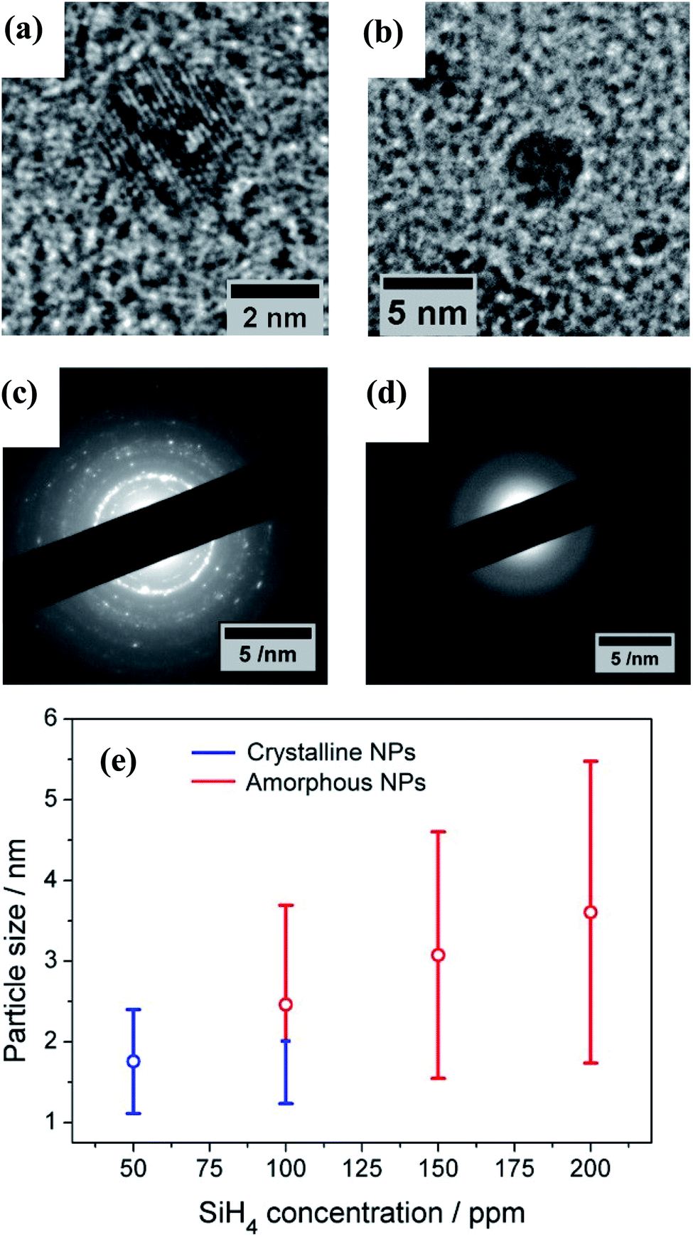 | ||
| Fig. 1 Transmission electron microscopy (TEM) characterization of the Si quantum dots (QDs). High resolution TEM of (a) a crystalline and (b) an amorphous Si QD. (c) and (d) Selected area electron diffraction (SAED) pattern of (c) crystalline and (d) amorphous Si QDs. (e) Mean particle size (dots) and standard deviation (bars) of the Si QDs as a function of the precursor concentration used; blue and red lines respectively denote the crystalline or amorphous character of the QDs within the size distribution. | ||
The XPS technique was used to chemically characterize the Si QDs produced under different experimental conditions. The photoelectron spectra in the Si 2p region are shown in Fig. 2a, along with a deconvolution of the peaks in the different oxidation states of Si. We can observe that only the crystalline samples show a higher binding energy shoulder, which can readily be associated with limited oxidation. On the contrary, samples which have a least a fraction of amorphous particles do not show this feature.
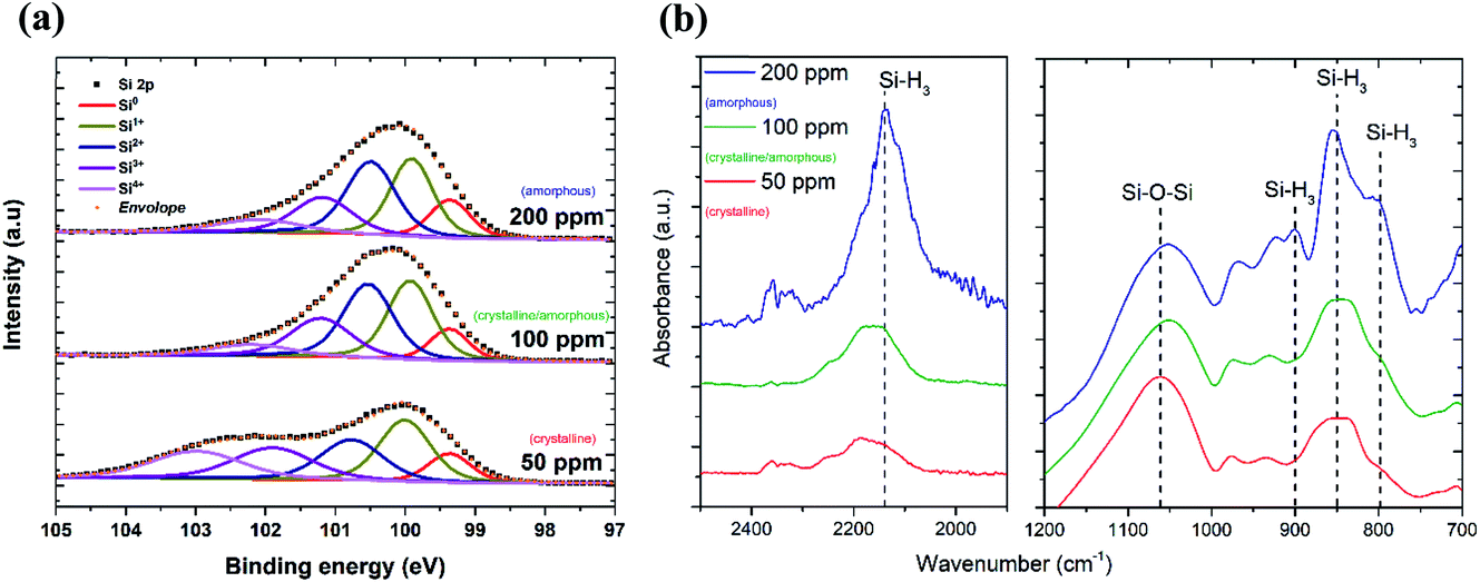 | ||
| Fig. 2 (a) Deconvolution of XPS Si 2p signal into components relative to the different oxidation states of Si atoms, reflecting an increased number of Si–O bonds with different coordinations for the sample with crystalline nanoparticles. (b) Fourier transform infrared (FTIR) spectra of Si QDs for the different precursor concentrations indicated. The dashed lines indicate vibrational transitions at wavenumbers 783 cm−1, 862 cm−1, 902 cm−1 and 2139 cm−1 and are associated with the Si–H3 bending, symmetric deformation, degenerate deformation and stretching modes, respectively, and a Si–O–Si absorption band at 1075 cm−1. | ||
Further details on the chemical composition of the Si QDs were obtained by FTIR analysis. Fig. 2b displays the FTIR spectra of Si QDs produced using the indicated SiH4 concentration in the plasma. In the two selected regions of the infrared spectrum shown in Fig. 2b, it is possible to observe the vibrations that correspond to Si–O and Si–Hx bonds. In particular, the absorption band at ∼1075 cm−1 associated with the Si–O–Si stretching mode is shown. This peak has a very strong absorption cross section and therefore the low absorbance (lower than the Si–Hx peaks) is evidence of a small level of oxidation even after exposure to the atmosphere. The peaks at 783 cm−1, 862 cm−1, 902 cm−1 and 2139 cm−1 are associated with the Si–H3 bending, symmetric deformation, degenerate deformation and stretching modes, respectively.28,29 The intensity of these peaks becomes significant for Si QDs synthesized using a high precursor concentration (200 ppm) which correspond to amorphous samples, while it is negligible for lower concentrations when the particles are crystalline. This suggests that when the synthesis is carried out using a silane concentration above 100 ppm, i.e. whenever some amorphous material is present, the particles become partially hydrogenated, possibly due to hydrogen incorporation within the QDs.16 In alternative, the amorphous particles may preferentially have silicon tri-hydride terminated surfaces as a result of the synthesis conditions.
We already reported the stability of Si nanocrystals through FTIR measurements in a previous study26 over a period of 30 days and concluded that these nanocrystals, while being H-terminated, tend to oxidize from the interaction of inserted oxygen backbonds (OxSi–H) and water vapour (e.g. from humidity in the air) condensing on the surface. However, this process is slow and self-limited, particularly when the QDs are deposited in films. Interestingly, the amorphous particles seem to be protected from oxidation at least in the first stages of exposure to the atmosphere (<1 h) and within the volume scoped by the XPS. This fact could be ascribed to the different kinetics of oxidation within amorphous particles30,31 or the higher H concentration and the ability of hydrogen to passivate dangling bonds more evenly than in the crystalline case. The degree of hydrogenation therefore seems to be important both in the oxidation process as well as at some level determining the phase of the QDs.
The XPS instrument also allows the acquisition of reflection electron energy loss spectra using the flood gun as an electron source. This technique can be used to easily ascertain qualitatively the presence of incorporated hydrogen within a sample, via an energy loss feature which sits around 1.8 eV from the zero-loss peak. In our case we observe a distinguishable peak for the conditions in which we obtain amorphous particles (100 ppm and 200 ppm) of SiH4 (Fig. S4, ESI†). We believe that under these conditions the level of hydrogenation is higher than in the other cases. When the QDs are crystalline (50 ppm), the presence of hydrogen is limited at the surface and for this reason the hydrogen reflection signal is essentially absent.
3.2 Formation mechanisms leading to the synthesis of Si QDs
We used a model to calculate the temperature at the surface of the Si QDs (Tp) during the synthesis process within the APP (see Section S6 in ESI†). Fig. 3 presents the estimated values of Tp corresponding to our synthesis conditions (black, red, green and blue squares); on the same graph we also plot the experimental crystallization temperature (CT, grey points) of Si QDs from the literature.32 The CT divides the graph into two regions: particles with a temperature below the CT are expected to be amorphous (blue region in Fig. 3) while particles with a temperature above the CT are expected to present a crystalline character (orange region in Fig. 3). Due to the intrinsic difficulty in measuring these values, it is not possible to define a sharp CT line to separate the two states.32 Instead, a transition region represented by a white band can be defined (see Fig. 3). It is possible to observe that for low SiH4 concentrations (50 ppm, black squares) the data points are all located entirely on the crystalline side of the graph. This result clearly agrees with the experimental evidence reported in Fig. 1, that is, the formation of purely crystalline Si QDs. For high precursor concentrations (>100 ppm) the opposite situation is observed. In this case, Tp is mainly located in the amorphous region with only the smallest, and less numerous, particles near the crystallization band. This is again in agreement with the experimental data in Fig. 1, where amorphous particles were observed under these conditions. The inability to produce a sufficiently high QD temperature for the crystallization of the Si QDs under these conditions can be partly attributed to the lower energetic plasma conditions (see Fig. S5†) but also to the larger particle size produced. At an intermediate SiH4 flow (100 ppm), only the smallest particles are located on the crystalline side and the rest lie on the crystallization band, as indeed confirmed by our QD characterization (Fig. 1). These results provide theoretical justification for the experimental observations, since only particles smaller than 2 nm were found to be crystalline in this intermediate condition.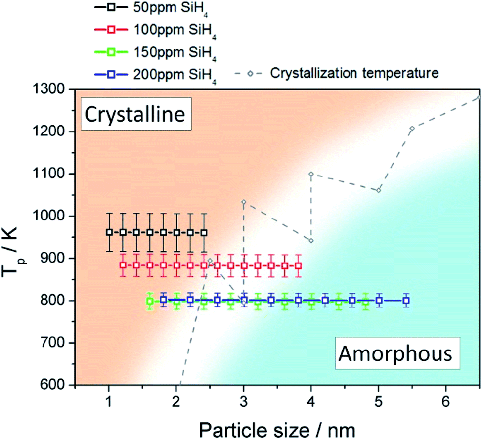 | ||
| Fig. 3 Particle temperature calculated using the collision-corrected model (CCM) for different concentrations of precursor introduced in the plasma and experimental crystallization temperature from ref. 32. The temperature has been calculated for the particle size distribution obtained for each condition. The crystallization temperature divides the graph into crystalline (orange) and amorphous (blue) regions. | ||
3.3 Valence band, Fermi level and bandgap measurements
The functional properties of semiconductors, in particular for energy applications, depend on the electronic structure and how the energy band parameters align with other application device components. We therefore perform here the experimental evaluation of energy band diagram (EBD) parameters such as valence/conduction band edges, Fermi level and bandgap for our samples. All measurements are therefore conducted on films of QDs deposited on solid substrates. Firstly, we focus on the valence band maximum (VBM) and Fermi level; in the next section we will complement these results with bandgap measurements to produce the EBD for both crystalline and amorphous QDs. To evaluate the electron energy levels near the valence band region and Fermi levels, we combined and compared results from different measurement techniques which offer different features, whose results are reported in Table 1.| Sample | Fermi level/eV | VBM/eV | E g/eV | |||
|---|---|---|---|---|---|---|
| E F-KP | E F-UPS | VBMUPS | VBMXPS | VBMAPS | E g-UVVIS | |
| 50 ppm | −6.0 ± 0.1 | −4.7 ± 0.1 | −5.9 ± 0.1 | −6.3 ± 0.6 | −5.7 ± 0.2 | 2.47 ± 0.07 |
| 100 ppm | −4.0 ± 0.1 | −4.3 ± 0.1 | −6.2 ± 0.1 | −6.4 ± 0.6 | −6.1 ± 0.2 | 2.6 ± 0.1 |
| 200 ppm | −3.9 ± 0.1 | −3.5 ± 0.1 | −5.7 ± 0.1 | −5.8 ± 0.6 | −5.8 ± 0.3 | 2.3 ± 0.1 |
UPS can be used to obtain the absolute value of the Fermi level of a semiconductor as well as the VBM. UPS measurements produce a cut-off energy (Ecut-off) and an on-set energy (Eon-set), which relate to the binding energy of electrons originating from the deepest levels of the material (ionized by the He–I source, hν = 21.22 eV) and from the valence band region, respectively (Fig. 4a). We should note that the UPS signal is referenced to the Fermi level of the semiconductor material under analysis. Therefore, the Fermi level can be extracted from the difference between Ecut-off and the energy of the He–I photons, i.e. EF-UPS = Ecut-off − 21.22 eV (see Table 1). The VBM is also calculated from the UPS measurements, where VBMUPS = EF-UPS − Eon-set (Table 1).
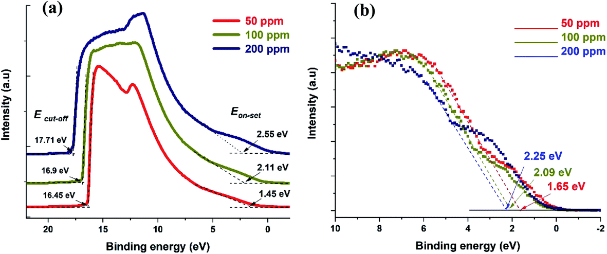 | ||
| Fig. 4 (a) UPS spectra for the three different samples showing both cut-off and on-set values. (b) XPS valence band spectra showing the difference between VBM and Fermi level. | ||
The Fermi level values obtained with the Kelvin probe show the same trend as those obtained by UPS, even though the values are different, and in one case (50 ppm) notably higher.
Meanwhile, XPS produces the difference between the Fermi level and the VBM (Fig. 4b). In order to determine the values of the VBM reported in Table 1, we used the Fermi levels obtained by UPS (also in Table 1). Finally, the APS technique is similar in principle to the lower energy range of the UPS, but it is operated under atmospheric conditions and the source is a deuterium lamp, which is not able to reach a cut-off in the photoemitted electrons. From the APS signal it is possible to extract an absolute value of VBM (see ESI Section S9†).
All the values summarized in Table 1 are also reported in Fig. 5. The comparison shows that discrepancies between different measurements do exist, which in most cases are within measurement uncertainties. Even differences above 0.1 eV can be significant for applications, however we should note that comparisons of different measurement techniques are seldomly reported in the literature and, as such, our results highlight and underline the difficulties and limitations of current and available measurement methods.
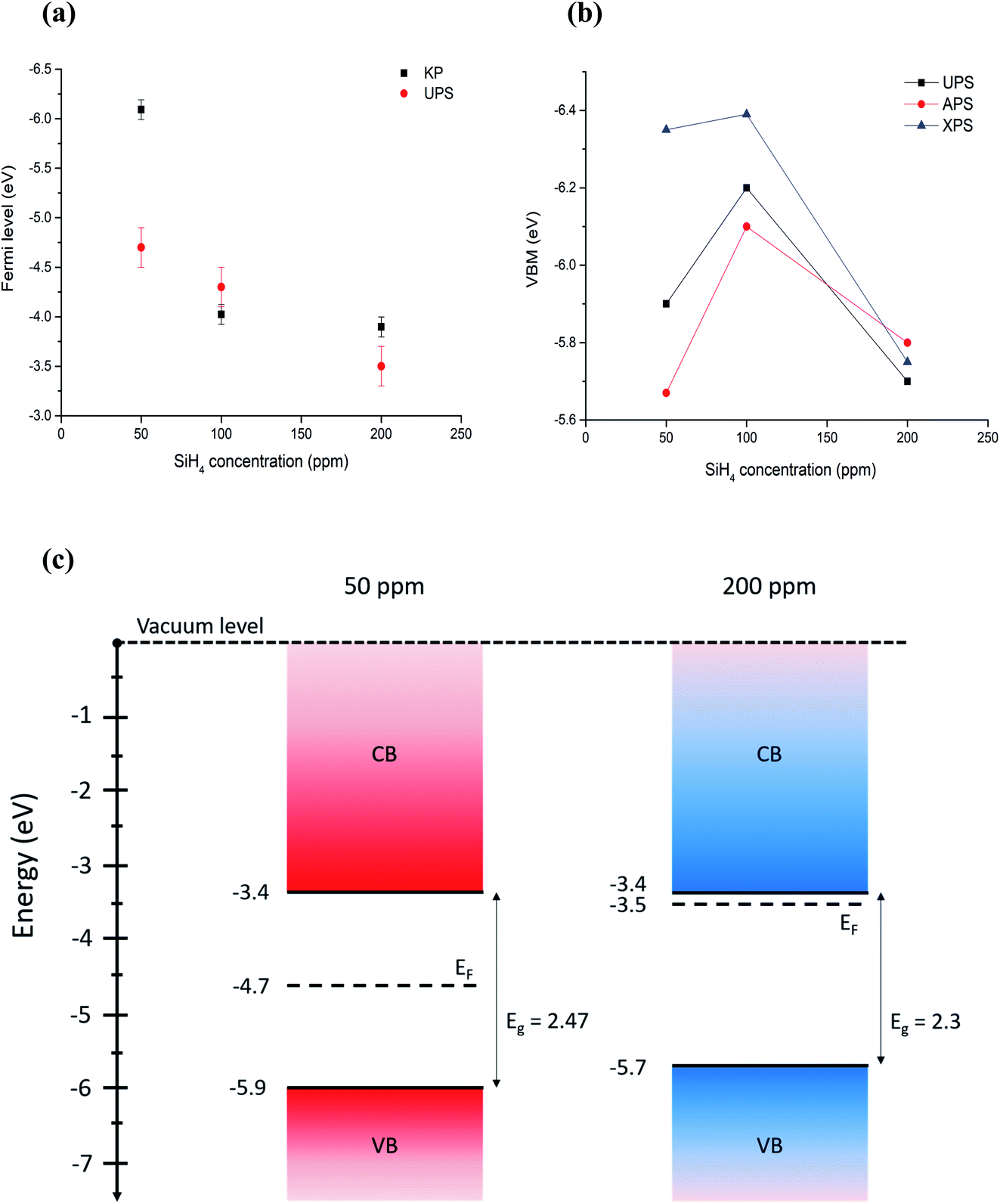 | ||
| Fig. 5 (a) Comparison of Fermi level measured with Kelvin probe and UPS. (b) Comparison of VBM values measured (UPS, APS) and calculated (XPS) using different techniques. Error bars are omitted for clarity and can be found in Table 1. (c) Energy band diagrams obtained combining UPS values for Fermi level and VBM, and energy bandgaps through Tauc plots for the extreme cases of 50 ppm and 200 ppm of silane, which correspond to the smallest (〈r〉 = 1.8 nm) all-crystalline particles and the biggest (〈r〉 = 3.6 nm) all-amorphous ones. | ||
With the exception of one of the measurements, the Fermi levels show similar values and exhibit the same trend, i.e. the Fermi energy becoming smaller with the particles going from crystalline to amorphous (Fig. 5a). The value of the Fermi level for the crystalline QDs (50 ppm) stands out and emphasizes the strong surface sensitivity of the KP technique (1–3 monolayers); while stray capacitance originating from inhomogeneities in the film can also impact the measurement, we tentatively ascribe this very large value of the Fermi level to the impact of even minor surface oxidation. The VBM values also show similar trends (Fig. 5b) with differences that can be justified by measurement uncertainties, with the exception of the VBM values of crystalline QDs (50 ppm) measured by XPS, which may be due to difficulties in extracting a good and reliable fit to the x-axis due to the limited resolution. A critical evaluation of the capabilities of each technique is therefore needed in order to determine which approach is most suitable and reliable in this specific case.
UPS measurements are implicitly limited by the general mechanism involved in photoemission as the light interacting with the sample induces a surface dipole, which complicates the evaluation of the Fermi level and VBM values, especially in conductive or highly doped samples.33 In our case we assume that the samples do not develop a particularly strong surface dipole, since we do not expect the samples to be highly conductive. However, the benefits of UPS technique depend on the high photoemission yield, the narrow energy resolution achievable and the ability to scope only the occupied electron states of the very top surface of a solid (2–3 nm). Instead, XPS in the valence band region suffers from moderate energy resolution, lower yields and the absence of an energy cut-off, which does not permit values to be obtained relative to the vacuum level and generally scopes a “deeper” region beneath the surface (5–10 nm).34 However, both techniques are operated in high vacuum, which can help to preserve the state of the surfaces.
KP and associated APS operating under atmospheric conditions are instead subject to surface dipoles and surface chemistry induced by environmental adsorbates which can easily shift the values up a few eV, raising or lowering the barriers felt by electrons escaping the material, or even induce completely new energy levels, especially in the valence electron region. These may be considered systematic errors in the values, which cannot be accounted for if there is not rigorous knowledge of the surface chemistry. While they are mostly useful for characterizing surfaces which will be exposed to the atmosphere (e.g. for corrosion studies), they also have the advantage of being cheap, easy and fast techniques. In addition, KP measurements are not affected by light-induced dipoles. However, APS operates under atmospheric conditions and photoelectrons experience different electrostatic environments as higher or lower potential barriers when escaping from the material surface.
These conditions depend on the atmospheric species and can change substantially with ambient temperature and humidity. In other words, while UPS and XPS relate to a potential energy of the ultra-high vacuum in the XPS chamber, the APS values relate to the electrostatic potential under atmospheric conditions at the time of measurement.35 It is clear that various techniques can be used for the determination of VBM and Fermi levels, however care should be taken in the selection of the most appropriate technique.
UV-vis transmission and reflectance spectra were acquired for the Si QDs. In all cases, the Si QDs exhibit continuous and relatively featureless optical characteristics. Transmission and reflectance measurements can be used to determine the bandgap of the Si QDs. A full description of the bandgap determination can be found in the ESI (Section S7†), which was calculated using Tauc plots, with a 1/2 coefficient corresponding to an indirect bandgap.36 A similar argument holds for amorphous silicon particles, for which the joint optical density of states is modeled by a square law.37,38 For low precursor concentrations (50 ppm), QDs present a bandgap of roughly 2.5 eV (see Table 1), and as previously observed (Fig. 1e) these experimental conditions generate crystalline particles. This value is consistent with H-terminated Si QDs in the size range reported (1.8 nm). However, for SiH4 concentrations greater than 100 ppm, the value at which we start to observe amorphous particles (Fig. 1e), the bandgap (more rigorously, the mobility gap) tends to a value of about 2.3–2.5 eV, which is consistent with the expected value for amorphous Si.39 The bulk bandgap of amorphous silicon is reported in the wide range of 1.6–1.97 eV, under conditions that strongly depend on the content of hydrogen and the degree of structural disorder introducing or relieving stress components. The relative importance of the two mechanisms is still debated.40–42 The higher values with respect to the bulk counterparts may be ascribed to quantum confinement effects, given the small particle size that we obtained. This fact can be either explained by an increased hydrogen content, which has been found in the REELS spectrum (Fig. S4 in ESI†). The 200 ppm silane samples, which resulted in the biggest amorphous-only particles, additionally show a long absorption tail to sub-bandgap energies that may be due to unsaturated bonds, ultimately acting as shallow dopant levels.
The surface photovoltage module in the KP can detect small amounts of photoinduced charge on a sample surface. The ability to build charge on the surface depends on both the light-induced bending of energy levels due to surface states, which results either in charge accumulation or depletion, and charge carrier mobilities.43 We observe a detectable photovoltage only in the samples with amorphous particles (see Fig. S8 in ESI†). The energy threshold for the appearance of a photovoltage shows similar values to the optical gaps (2.3 eV to 2.5 eV) found via UV-vis absorption, and the sign of the shift indicates that the samples have n-type behavior. This implies that charge transport within the layer of amorphous particles is superior with respect to the films of crystalline nanoparticles.43
3.4 Energy level diagram
Based on our discussion in Section 3.2, we can expect XPS and APS to be somewhat less accurate for the determination of the VBM. The former is because of a lower count and resolution at lower energies, which tends to overestimate the difference between the VBM and Fermi level, given the inability to resolve weaker signals. The latter is susceptible to environmental conditions and adsorbates to a higher degree than other techniques. For the same reason, Fermi level through the Kelvin probe may be equally dependent on the calibration value, which is obtained by the APS method and may be affected by ambient temperature, humidity and adsorbates on the particle surface.In conclusion, we believe that UPS values are more reliable for the determination of both the absolute Fermi level and the VBM, under the only assumption of a negligible light-induced surface dipole. Using energy bandgap values from UV-vis spectroscopy and UPS values, we have produced an energy band diagram of our single-phase samples (Fig. 5c).
The result is that, while the valence band maxima and bandgap do not vary significantly with the crystalline state of our nanoparticles, the value of the Fermi level tends to get closer to the conduction band edge with increased amounts of amorphous particles giving a stronger n-type character to the films. The UV-vis longer wavelength (sub-gap) absorption and the photovoltage response of amorphous samples support this picture.
4. Application as active layers in PV cells
Finally, in this section we provide some detail on the integration of Si QDs in photovoltaic (PV) devices. This is mainly to show that better knowledge of the EBD parameters can benefit application development, and also in part to demonstrate the capability of the APP process for direct integration of QDs in experimental devices. We have evaluated the performance of all-inorganic PV cells using the crystalline Si QDs synthesized with our method (50 ppm). The particles are directly deposited as a homogeneous film with the help of a two-axis stage placed 1 cm below the exit orifice of the capillary. Two device architectures were explored, both having Si QDs as the active component for the photogeneration of electron–hole pairs (see also ESI†).One of the device architectures is illustrated in Fig. 6a, the other in ESI S10.† We used indium-doped tin oxide (ITO) strip-coated glass (VisionTek Systems Ltd., 15 Ω sq−1, 150 nm ITO thickness) as our substrate and transparent conductive contact. A TiO2 layer (40 nm thick) is formed using a sol–gel method and spin-coating following the protocol previously described44 on top of the transparent conductive substrate. The TiO2 coated ITO-glass is then used as a substrate to directly deposit the Si QDs (3 μm thick film) exiting from the plasma reactor, using an X–Y stage to ameliorate the uniformity of the deposited layer. Spray-deposited Cu2O is then used as an electron blocking layer and a sputter-deposited gold film is used as a top contact. The non-equilibrated band diagram of the cell is shown in Fig. 6. We should note that the selection of the Cu2O transport layer was informed by our EBD measurements. The performance of the device was assessed with a solar simulator (Sub Femtoamp Keithley 6430) at standard AM1.5 irradiation. An open-circuit voltage and fill factor of 0.785 V and 87% were obtained, respectively. These are remarkable figures of merit that we can partly ascribe to exceptionally good energy level alignment of the Si QDs with the selected transport layer and contacts; however, the current density is very poor and affects the overall performance. Additionally, the measured value of series resistance is also indicative of relatively efficient electron transport in the cell (Table S10 in ESI†). Our current setup could not deliver thinner Si QD films as normally employed in this type of device; a reduction in the thickness could contribute to some improvements in the current density and overall device performance.
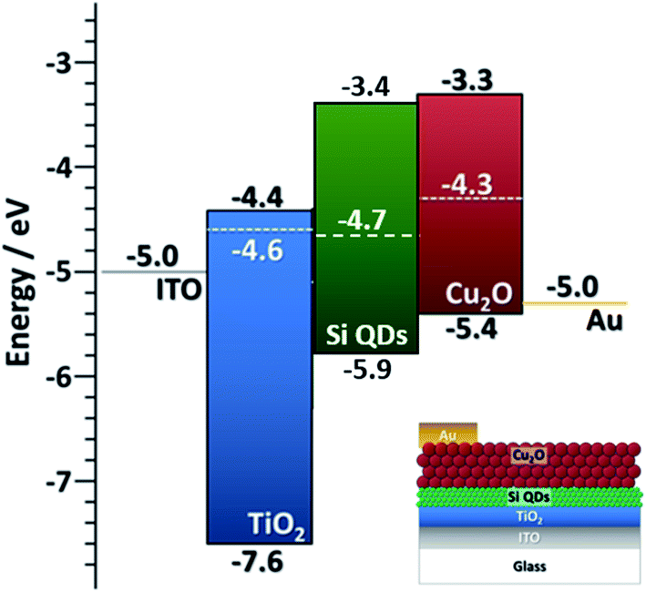 | ||
| Fig. 6 Non-equilibrated band diagram for the PV device based on Si QDs as active layers, Cu2O QDs as an electron blocking layer, a TiO2 film hole blocking layer and corresponding contacts. Inset: diagram of the layer structure of the device. | ||
While the overall performance remains very low, the device parameters are very encouraging and demonstrate the usefulness of careful EBD parameter analysis. The utilization of both amorphous and crystalline Si QDs for PVs remains debatable and recent trends show that further manipulation through surface modification, alloying or other methodologies will be required.45,46 In this context, the feasibility and integration of APP processes in the fabrication of next-generation devices is very promising and can give advantageous results.
5. Conclusions
We have demonstrated that Si QDs with tunable crystallinity can be grown in APPs. The study of a variety of experimental conditions has enabled us to produce Si QDs exhibiting crystalline or amorphous characteristics. The crystalline or amorphous character of the Si QDs was explained by efficient heating of the particles in non-thermal APPs. Analysis of the energy balance on the surface of the particles shows that the plasma parameters can be tuned to control the temperature of the particles when immersed in the plasma, and hence their crystallinity. We built an electron energy diagram of the valence electron regions for two selected samples, one with completely crystalline nanoparticles and one with completely amorphous nanoparticles and, after a critical assessment of measurements from different instruments, found that films formed from these free-standing particles tend to develop an n-type character for charge carriers in amorphous nanoparticles, despite similar values of valence band edges and optical bandgaps. We also showed the potential of APP processes for the fabrication of all-inorganic PV cells. Our analysis also highlights the need for improving analytical techniques and methodologies so that they could be used more extensively to dictate application-focused research directions.Conflicts of interest
There are no conflicts to declare.Acknowledgements
This work was supported by the EPSRC (EP/K022237/1, EP/M024938/1, EP/R008841/1) and the Leverhulme International Network (IN-2012-136).References
- F. Priolo, T. Gregorkiewicz, M. Galli and T. F. Krauss, Nat. Nanotechnol., 2014, 9, 19–32 CrossRef CAS.
- M. L. Mastronardi, E. J. Henderson, D. P. Puzzo and G. A. Ozin, Adv. Mater., 2012, 24, 5890–5898 CrossRef CAS.
- D. K. Kim, Y. Lai, B. T. Diroll, C. B. Murray and C. R. Kagan, Nat. Commun., 2012, 3, 1216 CrossRef.
- J. Park, L. Gu, G. von Maltzahn, E. Ruoslahti, S. N. Bhatia and M. J. Sailor, Nat. Mater., 2009, 8, 331–336 CrossRef CAS.
- V. Švrček, D. Mariotti, Y. Shibata and M. Kondo, J. Phys. D: Appl. Phys., 2010, 43, 415402–415410 CrossRef.
- D. Mariotti, S. Mitra and V. Švrček, Nanoscale, 2013, 5, 1385–1398 RSC.
- V. Švrček, M. Kondo, K. Kalia and D. Mariotti, Chem. Phys. Lett., 2009, 478, 224–229 CrossRef.
- V. Švrček, D. Mariotti and M. Kondo, Appl. Phys. Lett., 2010, 97, 161502 CrossRef.
- O. Wolf, M. Dasog, Z. Yang, I. Balberg, J. G. C. Veinot and O. Millo, Nano Lett., 2013, 13, 2516–2521 CrossRef CAS.
- M. Dasog, G. B. De los Reyes, L. V. Titova, F. A. Hegmann and J. G. C. Veinot, ACS Nano, 2014, 8, 9636–9648 CrossRef CAS PubMed.
- K. Kusova, et al. , ACS Nano, 2010, 4, 4495–4502 CrossRef CAS PubMed.
- V. Švrček, K. Dohnalova, D. Mariotti, M. T. Trinh, R. Limpens, S. Mitra, T. Gregorkiewicz, K. Matsubara and M. Kondo, Adv. Funct. Mater., 2013, 23, 6051–6058 CrossRef.
- D. M. Sagar, J. M. Atkin, P. K. B. Palomaki, N. R. Neale, J. L. Blackburn, J. C. Johnson, A. J. Nozik, M. B. Raschke and M. C. Beard, Nano Lett., 2015, 15, 1511–1516 CrossRef CAS.
- S. Askari, I. Levchenko, K. Ostrikov, K. P. Maguire and D. Mariotti, Appl. Phys. Lett., 2014, 104, 163103 CrossRef.
- S. Askari, M. Macias-Montero, T. Velusamy, P. Maguire, V. Svrcek and D. Mariotti, J. Phys. D: Appl. Phys., 2015, 48, 314002 CrossRef.
- S. Askari, V. Svrcek, P. Maguire and D. Mariotti, Adv. Mater., 2015, 27, 8011–8016 CrossRef CAS PubMed.
- R. Anthony and U. Kortshagen, Phys. Rev. B: Condens. Matter Mater. Phys., 2009, 80, 115407 CrossRef.
- Z. Shen, U. Kortshagen and S. A. Campbell, J. Appl. Phys., 2004, 96, 2204 CrossRef CAS.
- R. A. Street, Adv. Phys., 1981, 30, 593–676 CrossRef CAS.
- U. Kortshagen, J. Phys. D: Appl. Phys., 2009, 42, 113001 CrossRef.
- U. Kortshagen, L. Mangolini and A. Bapat, Nanotechnology and Occupational Health, 2006, 39–52 Search PubMed.
- L. Mangolini, E. Thimsen and U. Kortshagen, Nano Lett., 2005, 5(4), 655–659 CrossRef CAS.
- R. Gresback, Z. Holman and U. Kortshagen, Appl. Phys. Lett., 2007, 91, 093119 CrossRef.
- D. Mariotti and R. M. Sankaran, Perspectives on atmospheric-pressure plasmas for nanofabrication, J. Phys. D: Appl. Phys., 2011, 44, 174023 CrossRef.
- A. J. Wagner, D. Mariotti, K. J. Yurchenko and T. K. Das, Phys. Rev. E: Stat., Nonlinear, Soft Matter Phys., 2009, 80, 065401 CrossRef CAS PubMed.
- M. Macias-Montero, S. Askari, S. Mitra, C. Rocks, C. Ni, V. Svrcek, P. A. Connor, P. Maguire, J. T. S. Irvine and D. Mariotti, Nanoscale, 2016, 8, 6623–6628 RSC.
- S. Askari, M. Macias-Montero, T. Velusamy, P. Maguire, V. Svrcek and D. Mariotti, J. Phys. D: Appl. Phys., 2015, 48, 314002 CrossRef.
- F. S. Tautz and J. A. Schaefer, J. Appl. Phys., 1998, 84, 6636–6643 CrossRef CAS.
- Y. J. Chabal, Phys. B, 1991, 170, 447–456 CrossRef CAS.
- Z. H. Lu, E. Sacher and A. Yelo, Philos. Mag. B, 1988, 58, 385–388 CAS.
- A. Szekeres and P. Danesh, J. Non-Cryst. Solids, 1995, 187, 45–48 CrossRef CAS.
- A. N. Goldstein, Appl. Phys. A, 1996, 62, 33–37 CrossRef.
- M. M. Beerbom and B. Lagel, J. Electron Spectrosc. Relat. Phenom., 2006, 152, 12–17 CrossRef.
- S. Hüfner, Photoelectron Spectroscopy: Principles and Applications, Springer Science & Business Media, 2013 Search PubMed.
- A. Kahn, Mater. Horiz., 2016, 3, 7–10 RSC.
- J. Tauc, Mater. Res. Bull., 1968, 3, 37–46 CrossRef CAS.
- N. F. Mott and E. A. Davis, Electronic Processes in Non-Crystalline Materials, Clarendon-Press, Oxford, 1971 Search PubMed.
- M. L. Theye, Phys. Scr., 1989, T29, 157–161 CrossRef CAS.
- N.-M. Park, T.-S. Kim and S.-J. Park, Appl. Phys. Lett., 2001, 78, 17 Search PubMed.
- Y. Abdulraheem, I. Gordon, T. Bearda, H. Meddeb and J. Poortmans, AIP Adv., 2014, 4, 057122 CrossRef.
- A. M. Berntsen and W. F. van der Weg, Phys. Rev. B: Condens. Matter Mater. Phys., 1993, 48, 14656–14658 CrossRef CAS PubMed.
- G. D. Cody, T. Tiedje, B. Abeles, B. Brooks and Y. Goldstein, Phys. Rev. Lett., 1981, 47, 1480 CrossRef CAS.
- L. Kronik and Y. Shapira, Surf. Sci. Rep., 1999, 37, 1–206 CrossRef CAS.
- D. Carolan, C. Rocks, D. B. Padmanaban, P. Maguire, V. Svrcek and D. Mariotti, Sustainable Energy Fuels, 2017, 1, 1611–1619 RSC.
- V. Švrček, D. Mariotti, R. A. Blackley, W. Z. Zhou, T. Nagai, K. Matsubara and M. Kondo, Nanoscale, 2013, 5, 6725–6730 RSC.
- M. Bürkle, M. Lozac’h, C. McDonald, D. Mariotti, K. Matsubara and V. Švrček, Adv. Funct. Mater., 2017, 27, 1701898 CrossRef.
Footnote |
| † Electronic supplementary information (ESI) available. See DOI: 10.1039/c9fd00103d |
| This journal is © The Royal Society of Chemistry 2020 |