
Discordant nature of Cd in PbSe: off-centering and core–shell nanoscale CdSe precipitates lead to high thermoelectric performance†
Songting
Cai
 a,
Shiqiang
Hao
a,
Zhong-Zhen
Luo
bc,
Xiang
Li
d,
Ido
Hadar
b,
Trevor P.
Bailey
e,
Xiaobing
Hu
af,
Ctirad
Uher
e,
Yan-Yan
Hu
dg,
Christopher
Wolverton
a,
Vinayak P.
Dravid
*af and
Mercouri G.
Kanatzidis
*b
a,
Shiqiang
Hao
a,
Zhong-Zhen
Luo
bc,
Xiang
Li
d,
Ido
Hadar
b,
Trevor P.
Bailey
e,
Xiaobing
Hu
af,
Ctirad
Uher
e,
Yan-Yan
Hu
dg,
Christopher
Wolverton
a,
Vinayak P.
Dravid
*af and
Mercouri G.
Kanatzidis
*b
aDepartment of Materials Science and Engineering, Northwestern University, Evanston, Illinois 60208, USA. E-mail: v-dravid@northwestern.edu
bDepartment of Chemistry, Northwestern University, Evanston, Illinois 60208, USA. E-mail: m-kanatzidis@northwestern.edu
cSchool of Materials Science and Engineering, Nanyang Technological University, 50 Nanyang Avenue 639798, Singapore
dDepartment of Chemistry and Biochemistry, Florida State University, Tallahassee, Florida 32306, USA
eDepartment of Physics, University of Michigan, Ann Arbor, Michigan 48109, USA
fNUANCE Center, Northwestern University, Evanston, Illinois 60208, USA
gNational High Magnetic Field Laboratory, 1800 East Paul Dirac Drive, Tallahassee, FL 32310, USA
First published on 14th November 2019
Abstract
We report a novel hierarchical microstructure in the PbSe–CdSe system, which collectively contributes to significant enhancement in thermoelectric performance, with ZTave ∼ 0.83 across the 400–923 K temperature range, the highest reported for p-type, Te-free PbSe systems. We have investigated the local atomic structure as well as the microstructure of a series of PbSe–xCdSe materials, up to x = 10%. We find that the behavior of the Cd atoms in the octahedral rock salt sites is discordant and results in off-center displacement and distortion. Such off-centered Cd in the PbSe matrix creates (1) L–Σ electronic energy band convergence, (2) a flattened L band, both contributing to higher Seebeck coefficients, and (3) enhanced phonon scattering, which leads to lower thermal conductivity. These conclusions are supported by photoemission yield spectroscopy in air (PYSA), solid state 111Cd, 77Se NMR spectroscopy and DFT calculations. Above the solubility limit (>6%CdSe), we also observe endotaxial CdSe nano-precipitates with core–shell architecture formed in PbSe, whose size, distribution and structure gradually change with the Cd content. The nano-precipitates exhibit a zinc blende crystal structure and a tetrahedral shape with significant local strain, but are covered with a thin wurtzite layer along the precipitate/matrix interface, creating a core–shell structure embedded in PbSe. This newly discovered architecture causes a further reduction in lattice thermal conductivity. Moreover, potassium is found to be an effective p-type dopant in the PbSe–CdSe system, leading to an enhanced power factor, a maximum ZT of ∼1.4 at 923 K for Pb0.98K0.02Se–6%CdSe.
Broader contextThermoelectric (TE) devices can convert between thermal and electrical energy and are considered a promising energy-saving technology. Historically, PbSe has been considered as an inferior chalcogenide analog to PbTe, which is one of the top performing TE materials. The much larger abundance of Se compared to Te and higher melting point, however, make PbSe attractive for development with the aim of raising its performance closer to PbTe. This work demonstrates a synergistic combination of mechanisms in p-type PbSe brought about by the addition of CdSe to achieve an enhancement in the power factor and a concomitant reduction in the thermal conductivity, eventually yielding a high peak ZT of ∼1.4 with a record average ZTave ∼ 0.83 across 400–923 K. This significant advance is realized by all-scale microstructure construction via Cd alloying. Both theoretical and experimental results reveal that Cd2+ sits at an off-centered position in the PbSe lattice, leading to both electronic band convergence and low-frequency phonon modes. Moreover, tetrahedral CdSe nano-precipitates with core–shell architecture formed above the solubility limit, inducing significant strain and thus a further reduction in lattice thermal conductivity. The new insights into the exquisite role of Cd in PbSe provide better understanding for design of more efficient thermoelectric materials. |
Introduction
Thermoelectric (TE) devices are able to convert between thermal and electrical energy directly and reversibly,1,2 and are considered as a promising energy-saving technology thanks to their advantages such as no moving parts, service free operation and excellent environmental stability.3 Therefore, the desire to see TE applications more broadly implemented is strong, but these have been limited because of their high cost and low conversion efficiencies.4–6 The factors determining the conversion efficiency of TE devices are strongly interrelated and make performance improvements challenging.2,7–9 The efficiency of TE materials is determined by the figure of merit ZT = S2σT/κtot = S2σT/(κele + κlatt), where S, σ, T, κtot, κele and κlatt represent the Seebeck coefficient, electrical conductivity, absolute temperature, total thermal conductivity, electronic thermal conductivity and lattice thermal conductivity, respectively. The overall performance of TE devices, in fact, depends on the average ZT (ZTave), where (Th and Tc are the absolute temperature of the hot side and cold side, respectively). Therefore, in practical applications of thermoelectric materials in device modules, ZTave is the key figure of merit that determines the device efficiency, not the maximum ZT achieved at some temperature. ZTave must be as high as possible over as broad a temperature range as possible. In fact, the main reasons a high maximum ZT is generally pursued are derived from the desire to also obtain higher ZTave. Because most leading materials in this field contain rare and expensive tellurium (e.g. PbTe and Bi2Te3),10 there is a strong drive to develop next generation highly efficient, lower cost thermoelectric materials.11–13
During the past decade, remarkable milestones have been reached in enhancing ZT by improving the power factor (PF = S2σ),14–25 or reducing the lattice thermal conductivity. The latter was realized through the design of strengthened phonon scattering by hierarchical construction of microstructures, especially in lead chalcogenides,1,21,22,26–32 or by finding intrinsically low thermal conductivity in complex crystal structures.33–43 Lead telluride (PbTe) has a remarkable electronic conduction band (CB) and valence band (VB) and can be tuned by alloying into n-type (e.g. PbTe-CdTe,44 PbTe-PbS,45 PbTe-Ge/Si,46etc.) or p-type (e.g. PbTe-Mg/Ca/Sr,47 PbTe-PbS,48etc.). Because of the desire to reduce or eliminate the use of scarce tellurium, recently significant progress has been made in sulfide PbS analogs such as p-type Pb0.975Na0.025S–3%CdS (ZT ∼ 1.3 at 923 K)29 or n-type Pb0.9865Ga0.0125In0.001S (ZT ∼ 1.0 at 923 K).49 The enhanced performance in these Te-free systems is promising, but still inferior to PbTe. In contrast to PbTe, the PbSe analog has several noteworthy advantages: (1) a much larger abundance of Se and therefore lower cost, (2) a higher melting point and thus potentially a wider operation temperature range, and (3) lower lattice thermal conductivity. Hence, PbSe is a promising alternative for PbTe if one can tune its performance to a comparable level.50 The main disadvantage of PbSe relative to PbTe originates from its larger energy separation of the light hole L and heavy hole Σ valence bands (PbTe ∼ 0.14 eV, while PbSe ∼ 0.27 eV at room temperature), leading to lower power factors.
Zhao et al. reported effective strategies51 for improving the overall thermoelectric properties of p-type PbSe via CdS alloying and Na doping, where band convergence and nanostructuring were claimed to be responsible for the power factor enhancement and thermal conductivity decrease, respectively. Follow-up work by Tan et al. on the Pb1−xNaxSe–CdTe (p-type) system21 as well as by Qian et al. on Pb1−xSbxSe–CdSe (n-type)32 also gave record performance, which further proves the significant role Cd plays in PbSe. These previous studies only considered relatively low concentrations of Cd alloying and added other variables such as carrier dopants (Na or Sb) or anion substitution (Te or S) concurrently. Therefore, the exclusive effect of Cd on PbSe with respect to the solubility, micro/band-structure, phonon behavior, interactions with other dopants, etc. has not yet been addressed in any detail.
In this contribution, in an effort to decouple various factors involved in optimizing this system, and to better understand the role of Cd2+ in a rock salt lattice, we focused on PbSe–xCdSe compositions with large alloying concentration x up to 10%. With the help of solid-state NMR spectroscopy and DFT calculations, we probed the behavior of Cd atoms in PbSe solid solution sitting in the Pb sites of the rock salt structure. The previous studies did not address the local structure of Cd atoms in the lattice as it is generally assumed that it is a straightforward replacement of the octahedral Pb2+ atoms. However, the classical coordination chemistry of Cd2+ with chalcogen based ligands indicates that the tetrahedral coordination environment is strongly preferred. The following question then arises: is the Cd2+ ion stable in the perfect octahedral site imposed by the rock salt structure of PbSe? We expect an inherent conflict to exist between the tetrahedral coordination preference of Cd and the octahedral geometry of its hosting site, which could lead to significant local deviations, such as off-centering, in the structure from the ideal state. We refer to guest atoms found in this situation as discordant. In the present case, we find that the off-centering leads to both strengthened phonon-scattering in the low frequency regime and a converged, more flattened electronic band structure than in pure PbSe, all of which contribute to strongly enhanced thermoelectric performance. In addition, using advanced electron microscopy, we observe that above 6%CdSe content, CdSe precipitates in tetrahedral shape nucleate and form from the super-saturated solid solution. These have a zinc blende structure in their core and a wurtzite structure as a shell along the CdSe/PbSe phase boundary. This is a novel nanostructure and results in a further decrease of thermal conductivity due to induced significant local strain. Lastly, potassium doping is an effective p-type dopant in PbSe, leading to marked increases in the thermoelectric performance. The maximum ZT value of ∼1.4 is obtained in Pb0.98K0.02Se–6%CdSe, with a promising average ZTave of ∼0.83 at 400–923 K, which is the highest reported to date in a p-type, Te-free PbSe system.
Results and discussion
Phases and optical properties
The powder X-ray diffraction (PXRD) patterns of PbSe–xCdSe and Pb0.98K0.02Se–xCdSe (x = 0–10%) samples indicate that all peaks can be indexed to the rock-salt PbSe phase (space group: Fm![[3 with combining macron]](https://www.rsc.org/images/entities/char_0033_0304.gif) m, ICSD# 38294) with a slight shift to higher angle with increasing Cd concentration, see Fig S1(a) and (b) (ESI†). No second phases are observable within the detection limit of PXRD. Since the d-spacings of CdSe-ZB (CdSe-ZB, space group: F
m, ICSD# 38294) with a slight shift to higher angle with increasing Cd concentration, see Fig S1(a) and (b) (ESI†). No second phases are observable within the detection limit of PXRD. Since the d-spacings of CdSe-ZB (CdSe-ZB, space group: F![[4 with combining macron]](https://www.rsc.org/images/entities/char_0034_0304.gif) 3m, ICSD# 41528) and PbSe are extremely close, it is hard to conclude whether the shift of peaks comes from a second phase or lattice contraction after Cd substitution of Pb.
3m, ICSD# 41528) and PbSe are extremely close, it is hard to conclude whether the shift of peaks comes from a second phase or lattice contraction after Cd substitution of Pb.
The band gap of the materials increases from ∼0.24 eV for pure PbSe to ∼0.41 eV for PbSe–8%CdSe as determined by infrared absorption measurements, Fig. 1(a) and (b). The band gap of the PbSe–10%CdSe sample is slightly lower than that of the PbSe–8%CdSe sample, and the raw spectrum exhibits a noticeably different shape compared with the other samples, indicating that Cd might have reached its solubility limit in PbSe and created a second phase. The details of the CdSe solubility within PbSe will be discussed later.
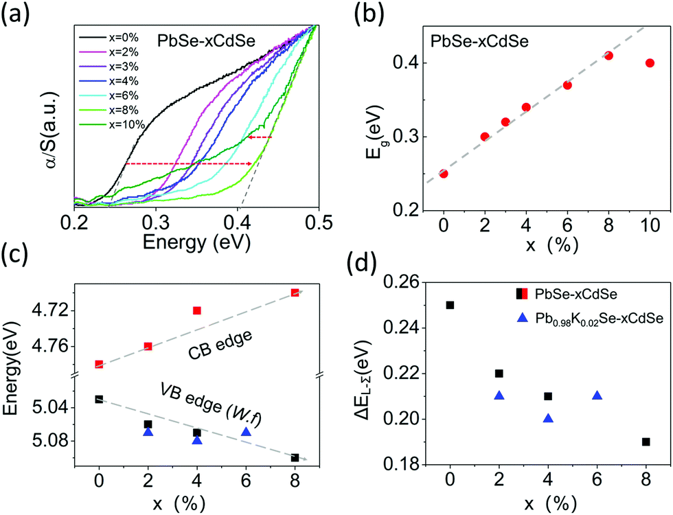 | ||
| Fig. 1 (a) Infrared absorption spectra for PbSe–xCdSe samples after SPS (spark plasma sintering). (b) Estimated electronic band gaps Eg. An increase of Eg can be observed from ∼0.24 eV for pure PbSe to ∼0.41 eV for PbSe–8%CdSe, followed by a slight decrease in PbSe–10%CdSe. (c) Energies of conduction band (CB) and valence band (VB) edges (work functions) for PbSe–xCdSe samples, shown in black and red squares, respectively. Three valence band edges for potassium-doped samples are shown in blue triangles. (d) Experimentally estimated energy differences between L- and Σ-valence bands, the error bars in these values are ±0.01 eV. | ||
To understand how Cd alloying modifies the electronic band edge positions of PbSe, we performed photoemission yield spectroscopy in air (PYSA) at room temperature. This technique determines the work functions of undoped PbSe–xCdSe and doped Pb0.98K0.02Se–xCdSe samples (for the spectra see Fig. S2, ESI†). The work function can be estimated by fitting the linear region of the spectra (see the ESI†). For undoped PbSe–xCdSe, with low carrier concentration, the work function essentially reflects the top of the L-valence band position versus a vacuum. Therefore, adding the measured band gap values to it gives the conduction band position, see Fig. 1(c). These results clearly indicate that the band gap widening is attributed to both the valence band edge moving deeper in energy (from 5.03 eV for pure PbSe to 5.10 eV for PbSe–8%CdSe) and the conduction band moving higher in energy (from 4.78 eV for pure PbSe to 4.70 eV for PbSe–8%CdSe). The work functions of several potassium-doped samples show a slight increase in energy, indicating that the top of the L-valence band moves slightly lower. Assuming that the Σ-valence band position remains unchanged (supported by DFT calculations shown in Fig. 5(c)), we can then estimate the energy offset between the L- and Σ-bands (ΔEL–Σ) in different samples based on the fact that ΔEL–Σ of pure PbSe is ∼0.25 eV.25 ΔEL-Σ decreases from 0.25 to 0.19 eV as seen in Fig. 1(d). This value approaches the 0.15 eV ΔEL–Σ value of PbTe.
Discordant Cd atoms in PbSe probed with DFT calculations and solid-state NMR
It is known that the vast majority of Cd chalcogenide compounds including CdSe in the wurtzite and zinc blende crystal structure have Cd atoms in tetrahedral sites surrounded by Se atoms.52,53 Therefore, substituting Pb with Cd in PbSe will lead to an uncommon and destabilizing octahedral environment for Cd. Intuitively, Cd might tend to shift its lattice position from the center of the octahedral site to lower its energy. Density functional theory (DFT) calculations indicate that when the Cd atoms shift away from the lattice-imposed octahedral center, the overall energy of the system does decrease. The results suggest that a shift of ∼0.01 Å away from the octahedral center along the [111] direction brings the system to the minimum total energy, Fig. 2(a) and (b). In addition, the existence of negative frequencies in the DFT-calculated phonon dispersion curves when placing Cd at the center of the PbSe lattice (Fig. 7(b)) also indicates instability of the on-centered Cd atoms and a tendency for off-center displacement. This aspect will be discussed in more detail later.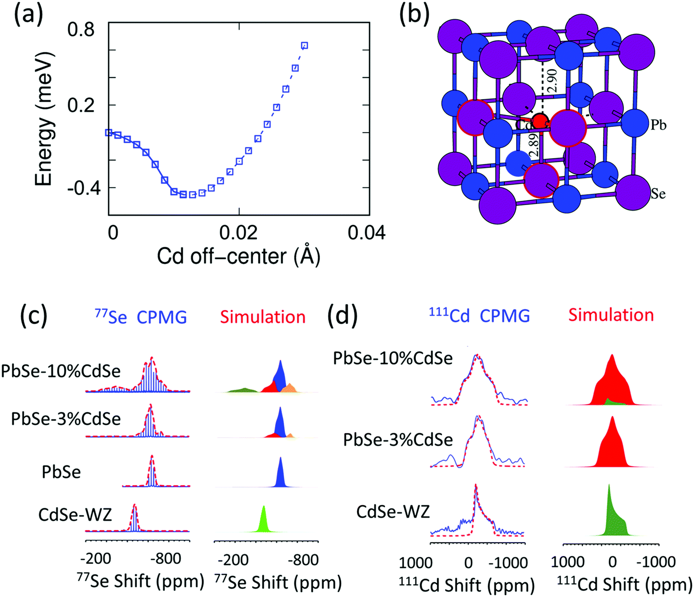 | ||
| Fig. 2 (a) System energy change with respect to the Cd off-centering distance from the octahedral site center along the [111] crystallographic direction. A local minimum is reached when the displacement is ∼0.01 Å. The energy profile shown as a solid line from a regular octahedral site to a local minimum off-centered site is calculated by the Nudged Elastic Band method,56 while the dashed line away from the off-center position is evaluated by static DFT calculations. (b) Local atomic structure of off-centered Cd in PbSe. (c) 77Se CPMG static NMR spectra and the corresponding simulations of CdSe-WZ, PbSe, PbSe–3%CdSe and PbSe–10%CdSe. (d) 111Cd NMR spectra and the corresponding simulations of CdSe, PbSe–3%CdSe, and PbSe–10%CdSe. The NMR parameters used for the simulation are listed in Tables S1 and S2 (ESI†). | ||
We employed solid-state NMR spectroscopy as a powerful tool to probe the local structural environment of 77Se as well as 111Cd.30,52,54,55 We used the Carr–Purcell–Meiboom–Gill (CPMG) pulse sequence to acquire 77Se NMR, in order to enhance the spectral sensitivity as well as to achieve broad band excitation. The static 77Se CPMG NMR spectra together with the corresponding simulations of CdSe, PbSe, PbSe–3%CdSe and PbSe–10%CdSe phases are shown in Fig. 2(c). The 77Se NMR spectrum of wurtzite CdSe shows only one component with an isotropic shift of −470 ppm and a small shift anisotropy of 35 ppm. The 77Se NMR spectrum of PbSe exhibits a resonance at −635 ppm with a shift anisotropy of 37 ppm. The relatively small 77Se NMR shift anisotropies of both CdSe and PbSe are due to their high coordination symmetry. Once a small amount of Cd is alloyed into PbSe, line broadening with changes in the 77Se shift are observed. A more complex 77Se NMR spectrum with 3 components is obtained for PbSe–3%CdSe. The chemical shift differences among these three components reflect the different electronic environments. The major component resonating at −632 ppm is assigned to PbSe with a slightly increased shift anisotropy from 37 ppm to 48 ppm, indicating a more disordered Se structural environment than in pure PbSe. The two minor broad resonances are likely from Se directly coordinated to Cd at an off-center position. Specifically, one resonance at −560 ppm is assigned to Se atoms closer to the adjacent discordant Cd atoms. The other minor resonance at −720 ppm reflects Se atoms lying farther apart from Cd atoms. As the Cd fraction increases from 3% to 10%, the above-mentioned resonances continue to be observed but the off-center components become stronger. As seen in Table S1 (ESI†), the shift anisotropy parameter used in the simulation significantly increases for all three sites. An additional broad 77Se resonance, however, is observed at −275 ppm with a shift anisotropy of 140 ppm for the PbSe–10%CdSe sample, which is assigned to wurtzite CdSe and zinc blende CdSe occurring as second phases.
More direct Cd structural information can be extracted from the 111Cd NMR spectra of CdSe, PbSe–3%CdSe, and PbSe–10%CdSe, as shown in Fig. 2(d). The 111Cd NMR spectrum of the CdSe sample shows a resonance at −230 ppm with a shift anisotropy of 310 ppm. As Pb is replaced by Cd in PbSe–3%CdSe, one broad resonance is observed with a shift anisotropy of 390 ppm, implying the solid-solution state formed after Cd alloying. With a further increase of the Cd content (PbSe–10%CdSe), the shift anisotropy significantly increases from 390 ppm to 480 ppm, indicating a more asymmetric Cd local environment. In addition, a minor broad component appears resonating at −220 ppm because of second phase formation of extra CdSe, which agrees with the 77Se NMR results presented above and the TEM results to be discussed later. Therefore, it can be concluded that Cd atoms in PbSe are off-centered from exactly in the octahedral site.
Novel nanostructuring in PbSe–xCdSe materials
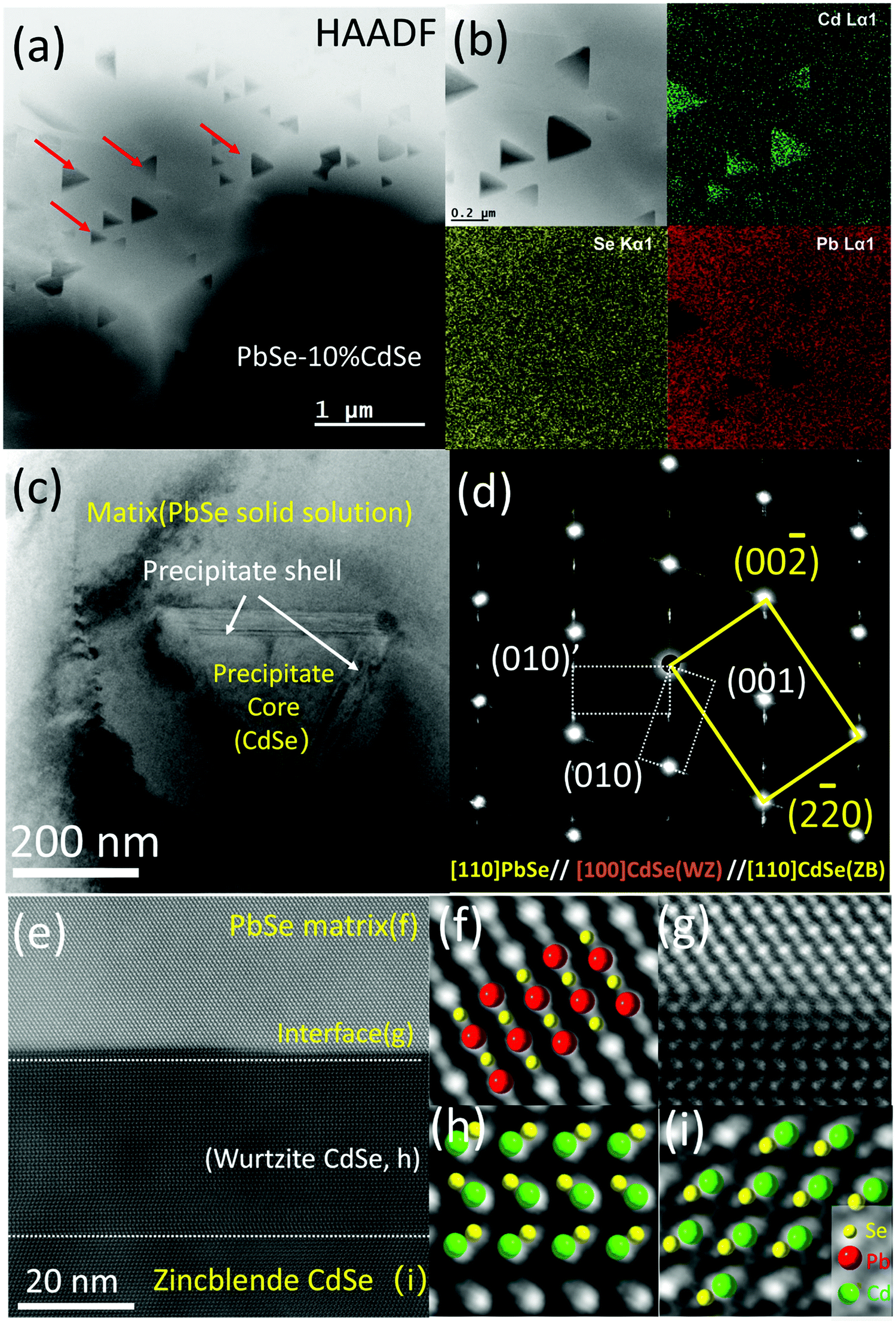 | ||
| Fig. 3 Scanning/transmission electron microscopy (S/TEM) analyses of PbSe–10%CdSe. (a) High-angle annular dark field image. A large amount of triangular nano-precipitates is embedded within the grains of the matrix. (b) EDS mapping of a selected area in (a). (c) Typical TEM image of a precipitate sitting in the matrix. The diffraction contrast highlights three different regions: the matrix, the main body of the precipitate and ∼20 nm thick layers as shells between the interfaces. (d) Selected area diffraction pattern (SAED) taken along the [110] zone axis of the matrix, revealing that the interface is the wurtzite CdSe phase. (e) High-resolution STEM image (HRSTEM) with a HAADF mode image of one edge of the precipitate and the matrix. The atomic stacking of the matrix, the matrix–shell interface, the shell, and the core of the precipitate is highlighted in (f)–(i), respectively. | ||
Fig. 3(c) is a low magnification bright field TEM image with one precipitate situated in the matrix. Clearly, the diffraction contrast in the image divides the specimen into three regions, namely the matrix, the main body of the precipitate and two ∼20 nm thick bands sandwiched between the interfaces. The selected area diffraction pattern (SAED) including all three regions in Fig. 3(c) is shown in Fig. 3(d). The main brightest spots belong to rock-salt PbSe (space group: Fmm, ICSD# 38294) and zinc blende CdSe phases (CdSe-ZB, space group: F3m, ICSD# 41528) along the [110] zone axis. Since the difference in lattice parameter between these two phases is very small (a = 6.128 Å for PbSe and a = 6.077 Å for CdSe-ZB), diffraction spot splitting can only be seen far away from the transmission beam. It should be noted that under our synthesis methods, the main CdSe second phase precipitated out from the PbSe matrix is the zinc blende structure, while the thermodynamically stable phase for CdSe is actually wurtzite.53 The streaking and the two sets of extra spots observed along the {111} planes of the matrix belong to the hexagonal wurtzite CdSe phase (CdSe-WZ, space group: P63mc, ICSD# 415784) along the [100] zone axis. The series of dark field images in Fig. S3 (ESI†) further reveal that the wurtzite CdSe diffraction spots come exclusively from the two bands in the interface between the PbSe and the CdSe phase.
To visualize the atomic arrangement as well as additional details in the interface region, we employed aberration corrected (probe) high-resolution STEM imaging. Fig. 3(e) is a typical HAADF image taken along the [110] zone axis of the matrix, revealing endotaxial precipitation. From the zoom-in versions shown in Fig. 3(f)–(i), the differences in atom stacking can be easily seen. Atoms in the PbSe solid solution region and the core of the CdSe precipitate (zinc blende CdSe) exhibit ABC/ABC stacking but turn into AB/AB in the hexagonal wurtzite phase at the shell (wurtzite CdSe). Moreover, several stacking faults can be observed within the shell because of the small energy cost for stacking fault formation.58
We performed similar studies on the PbSe–8%CdSe and PbSe–6%CdSe samples. In particular, precipitates with the exact same shape but smaller size (∼20 nm) are observed in the 8%CdSe sample, see Fig S4(a) and (b) (ESI†). The shell at the interface here is around ∼7–8 atomic layers. For the PbSe–6%CdSe sample, as shown in Fig. S5 (ESI†) of a triple junction of three grains, the elements distribute homogeneously both inside the grain and along the grain boundaries. The high-resolution TEM image and the SAED diffraction pattern further confirm the formation of the PbSe–CdSe solid solution. Taken together, the solubility of CdSe in un-doped PbSe is above 6% under such synthesis and processing methods. Above the solubility limit, endotaxial tetrahedral precipitates with core–shell architecture can be observed, whose size increases from ∼20 nm to ∼200 nm when the CdSe concentration changes from 8% to 10%.
Fig. 4(a) is a typical dark field TEM image of Pb0.98K0.02Se–6%CdSe, highlighting a significant number of very small (∼5 nm) precipitates embedded in the matrix. The SAED pattern inset confirms its rock-salt PbSe phase, and the image is taken along the [110] zone axis. Although no extra spots can be detected, there is significant diffuse diffraction, indicating a high degree of strain in the sample. Moreover, according to the high-resolution TEM image in Fig. 4(b), these precipitates also exhibit the same tetrahedral shape as the ones described above, but with no wurtzite shell being present at the interface. The absence of the wurtzite shell in this sample may be due to the smaller size of the precipitates (caused by the presence of K, indirect influence), or the direct influence of K. In addition, we observe obvious microstructural differences between this work and previously reported PbSe–Cd systems.21,32,51 These differences may originate from the different dopants used in the samples as well as possible artifacts from ion-beam damage during TEM sample preparation in some previous studies.59
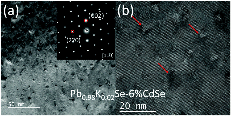 | ||
| Fig. 4 (a) Bright field TEM image of Pb0.98K0.02Se–6%CdSe taken along the [110] zone axis. A large amount of triangular precipitates of ∼5 nm in size can be observed. The inset is the selected diffraction pattern. (b) High-resolution TEM image of a selected area in (a), revealing the coherent interface between the zinc blende CdSe second phase and the PbSe matrix. | ||
With increasing CdSe amount in the samples, micron-scale CdSe second phases with irregular shapes appear, as shown in the STEM image for Pb0.98K0.02Se–8%CdSe in Fig. S7 (ESI†). Given the shape of the second phase and the elemental distribution, its formation may be via a different mechanism. For example, the added potassium could shift the eutectic point of the PbSe–CdSe system to lower temperature, which would cause the CdSe second phase to nucleate already from the liquid phase when its concentration is high.
Boosting thermoelectric performance via K doping
Although typically Na is the standard p-type dopant used in lead chalcogenides, K doping is much less investigated and in previous work it has been shown to be an effective dopant.60–62 We therefore decided to use it in this work for the first time in a PbSe–CdSe based system. Fig. 5(a) and (b) show the temperature-dependent (300 K–923 K) electronic properties of Pb0.98K0.02Se–xCdSe (x = 0–10%). All samples behave as degenerate semiconductors, where the electrical conductivities (Fig. 5(a)) decrease at elevated temperatures because of electron–phonon scattering. A noticeable deviation from the normal σ ∼ 1/T relationship is observed in the low temperature range (300–500 K) and it is attributed to grain boundary scattering,63 which is diminished in the high temperature region where the thermoelectric properties are most interesting. At room temperature, σ significantly decreases with rising Cd concentration typically from ∼3100 S cm−1 in Pb0.98K0.02Se to ∼950 S cm−1 in Pb0.98K0.02Se–6%CdSe.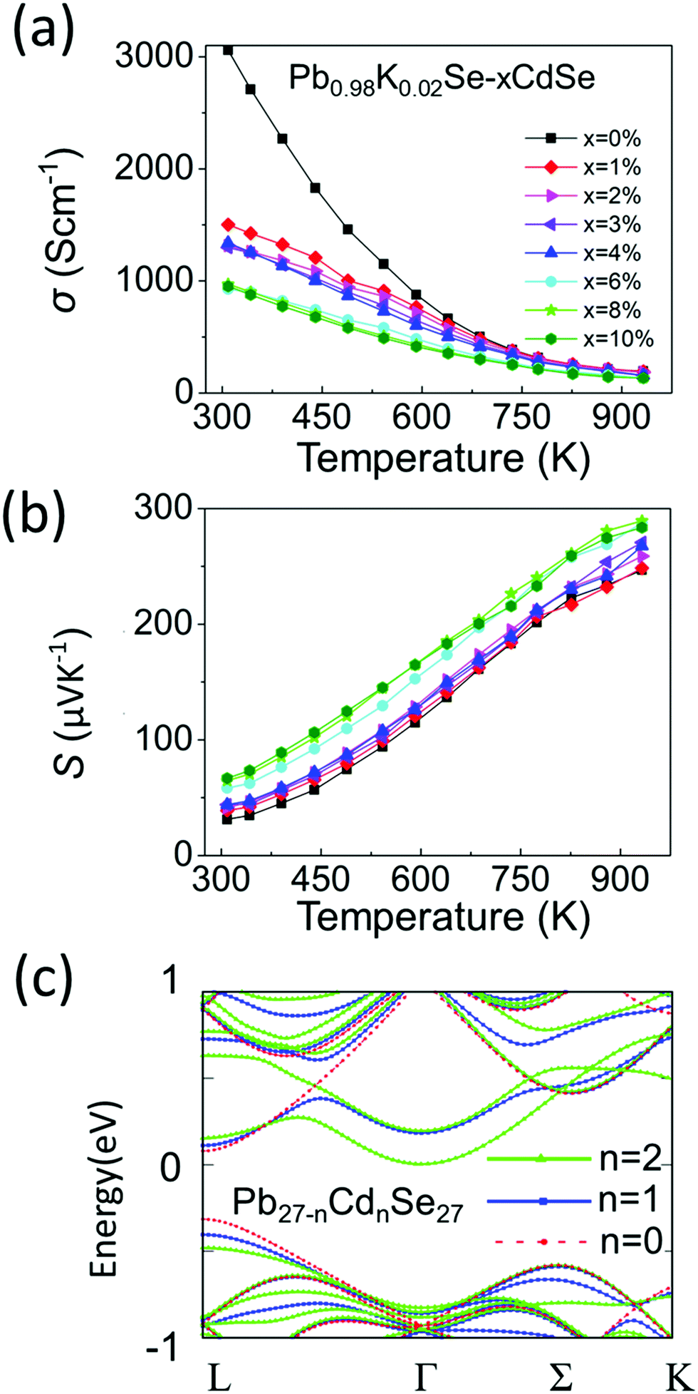 | ||
| Fig. 5 (a) and (b) Temperature-dependent electrical conductivity and Seebeck coefficients for Pb0.98K0.02Se−xCdSe (x = 0–10%). (c) DFT calculated band structures for the Pb27-nCdnSe27 supercell, where n = 0, 1, 2. | ||
The Seebeck coefficients are positive, indicating that they are p-type semiconductors with holes as the dominant carriers, Fig. 5(b). Specifically, the Seebeck coefficient gradually increases with increasing CdSe amount up to 6%. The highest coefficient of ∼290 μV K−1 is obtained in Pb0.98K0.02Se–6%CdSe at 923 K.
To better understand the nature of the electronic structure and the enhanced Seebeck coefficient, we performed DFT calculations on both PbSe–CdSe and pure PbSe, Fig. 5(c). Compared to pure PbSe, two important changes can be seen after adding Cd into the matrix: first, a lower energy offset between the L and Σ bands (from 0.27 to 0.15 eV, band convergence) induces a larger band gap (the energy offset between the conduction band and L band, ΔEc-L). This result has been confirmed experimentally by the optical band gap and work function measurements discussed above. Second, adding Cd leads to noticeable flattening of the L band. The flattened band results in an increased effective mass relative to PbSe (from 0.27 to 0.65me), as shown in Table S3 (ESI†). Indeed, such an increase in m* is experimentally supported by the room temperature Hall measurements, see Table S4 (ESI†). Based on the Pisarenko relation and assuming a single parabolic band contributing to carrier conduction, we calculated the room temperature effective masses for the samples. In agreement with the simulations, the Cd containing sample exhibits a dramatic increase in effective mass. Specifically, the effective mass of Pb0.98K0.02Se is ∼0.31me, consistent with the value reported in other pure PbSe samples elsewhere.51 However, the effective mass of the sample with 6%CdSe is estimated as 3× higher, reaching ∼1me. Both the band convergence and band flattening are therefore beneficial for enhancing the Seebeck coefficient. Combining the Seebeck coefficient with the electrical conductivity results, a high power factor of ∼14 μW cm K−1 is obtained at 723 K for Pb0.98K0.02Se–2%CdSe (Fig. S8, ESI†).
To decouple the effect of K doping and Cd alloying on the thermal transport behavior, we studied the temperature-dependent thermal properties of doped and un-doped PbSe–xCdSe. Fig. 6(a) shows the temperature-dependent total thermal conductivity data for the undoped PbSe–xCdSe (x = 0–10%) sample. Since no significant electron/hole carriers are present, all samples behaved as non-degenerate semiconductors with decreasing thermal conductivity as the temperature increases and apparent bipolar diffusion occurred above 600 K. Therefore, the total thermal conductivities reflect the lattice phonon conductivity with negligible contribution from the electronic part. Notably, the bipolar diffusion in all Cd-alloyed samples is clearly suppressed compared to pure PbSe because of the widening of the electronic band gap. Moreover, κtot of the samples gradually decreases up to 8%CdSe, followed by a slight increase for the PbSe–10%CdSe sample. Specifically, compared with pure PbSe having κtot ∼1.8 Wm−1 K−1 at room temperature, κtot of the 3% (∼1.5 Wm−1 K−1), 6% (∼1.3 Wm−1 K−1) and 8% (∼1.1 Wm−1 K−1) samples has dropped ∼16%, ∼25% and 40%, respectively.
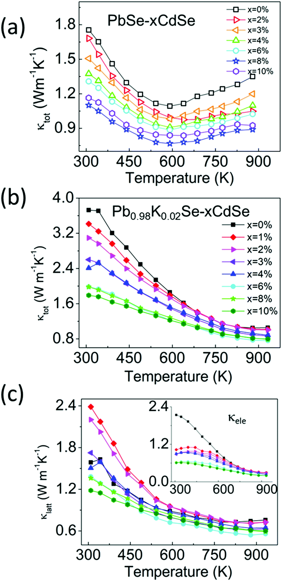 | ||
| Fig. 6 Temperature-dependent (a) total thermal conductivity of PbSe–xCdSe (x = 0–10%) and (b) and (c) total thermal conductivity and lattice thermal conductivity of Pb0.98K0.02Se–xCdSe (x = 0–10%), respectively. The lattice thermal conductivity of these samples was determined by subtracting the electronic part from κtot, namely κlatt = κtot − κele, where κele is calculated based on the Wiedemann–Franz law κele = LσT, with L the Lorenz number.64 | ||
In comparison, the temperature-dependent thermal transport properties for the samples of Pb0.98K0.02Se–xCdSe (x = 0–10%) are shown in Fig. 6(b). Generally, the total thermal conductivity of the samples significantly decreases as the CdSe fraction increases. Typically, the κtot of ∼3.8 Wm−1 K−1 drops to ∼2.0 Wm−1 K−1 for Pb0.98K0.02Se–6%CdSe, and to ∼1.8 Wm−1 K−1 for Pb0.98K0.02Se–10%CdSe. The lowest total thermal conductivity of ∼0.8 Wm−1 K−1 is obtained in the 6%CdSe sample at 923 K with a corresponding lattice thermal conductivity of ∼0.6 Wm−1 K−1.
To explore the primary physical reasons for Cd inducing the significant lattice thermal conductivity reductions observed, we performed DFT-based phonon calculations using a structure model with discordant Cd atoms in PbSe. In this model the calculated phonon dispersions indicate a much lower vibration frequency for the acoustic branches compared to pure PbSe, resulting in a lower longitudinal Debye temperature, Fig. 7(a). Moreover, the average phonon velocity of the Cd-alloyed PbSe structure is about 2300 m s−1, much lower than the 2614 m s−1 for pure PbSe. In addition, compared to the pure PbSe, the relatively strong attraction of the off-centered Cd with its nearest Se atoms induces longer bonds between the next nearest neighbor Pb (Pb NN) and Se. Because the calculations indicate that the Pb and Cd atoms contribute the most to the acoustic phonon transport (frequency < 40 cm−1) with a negligible role played by Se, only changes in Pb will be considered here.
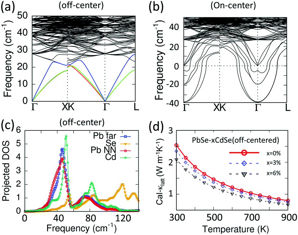 | ||
| Fig. 7 (a) Phonon dispersion curves (on the Pb26CdSe27 supercell) with acoustic branches highlighted with different colors. (b) Phonon dispersion curves of PbSe with Cd sitting on the center of the octahedral site (on-center). Significant imaginary frequencies exist, indicating instability of such a structure. (c) Corresponding projected density of states (DOS) of PbSe with off-centered Cd in the matrix (off-center). The density of states from next nearest neighbor Pb atoms (Pb NN, red line) is shifted to the low frequency regime compared with the ones lying farther away from Cd atoms (Pb far, blue line). (d) DFT-calculated lattice thermal conductivity of off-centered PbSe–CdSe with different concentrations of Cd. | ||
The discordant Cd atom creates a strong local strain field affecting not only its own coordination environment but also the next nearest neighbor Pb atoms, as shown with the red line in Fig. 7(c). These low frequency vibrations are even lower than those of other Pb atoms lying farther (Pb far) from the Cd atoms, which are shown with the blue line. As a result, the discordant Cd and the induced distorted local Pb environments synergistically contribute to lowering the lattice thermal conductivities. This is illustrated by the DFT-calculated lattice thermal conductivity of the off-centered structure in Fig. 7(d). As a comparison, the phonon dispersion curves of PbSe with Cd sitting on the center of the octahedral site (on-center) were calculated, see Fig. 7(b). It is known that the acoustic modes are considered for lattice thermal conductivity calculations in the Debye–Callaway methods, where accurate Grüneisen parameters, phonon velocities and Debye temperatures are necessary. However, for a phonon dispersion with significant imaginary frequencies indicating instability of such an on-center structure, the above parameters are not correct and hence the lattice thermal conductivity cannot be evaluated.
Collectively, in the solid solution samples with <6%Cd, we attribute the significant decrease of the thermal conductivity to the discordant Cd atom nature and the corresponding local distorted Pb atomic environment. Above the solubility limit, a further decrease of κlatt comes from the faceted nano-precipitates in the range 5–50 nm. Any differences observed between the doped and un-doped samples mainly originate from solubility and microstructure changes.
Combining the improved electronic and thermal properties presented above, a remarkable gain in the overall thermoelectric performance is obtained, as shown in the temperature-dependent ZT of Pb0.98K0.02Se–xCdSe (x = 0–10%). Specifically, a ZT of ∼1.4 at 923 K is achieved for the 6%CdSe sample, higher than all other concentrations owing to the appearance of nano-precipitates that diminish the thermal transport. Because of the band flattening effects, the Seebeck coefficient and ZT from 300–500 K are higher than previous studies on PbSe. This leads to a high average ZTave of ∼0.83 (400–923 K), the highest reported value in p-type, Te-free PbSe-based systems.30,51,65 This is a significant figure of merit because it is slightly lower or even comparable to most PbTe-based materials and relevant to obtaining high conversion efficiency in devices (Fig. 8).44,47,66,67
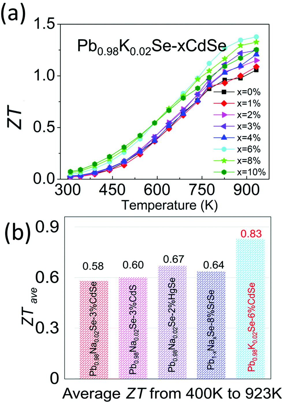 | ||
| Fig. 8 (a) Temperature-dependent ZT of Pb0.98K0.02Se–xCdSe (x = 0–10%) samples. (b) Comparison of average ZT (ZTave) from 400–923 K among state-of-the-art p-type, Te-free PbSe systems.30,51,65 | ||
Concluding remarks
The insertion of Cd in octahedral Pb sites in the rock-salt structure of PbSe causes strong local distortion in the coordination environment of Cd because of its preferred tetrahedral binding. The Cd atoms are discordant with the Pb sites in the rock-salt lattice and prefer the off-centered position close to ∼0.01 Å away from the normal octahedral center based on solid state NMR spectroscopy and DFT calculations. The induced distorted local Pb environments contribute to lower lattice thermal conductivities. The Cd alloying also leads to bandgap enlargement, L–Σ band convergence and L band flattening, enhancing the Seebeck coefficient. Above the solubility limit of 6%, CdSe nucleates and grows in the PbSe matrix as a second phase. The tetrahedral nano-precipitates show a core–shell morphology with a zinc blende structure inside and wurtzite outside along the phase boundary. This is a novel three-phase nanostructure and further contributes to depressed thermal transport when the precipitate size is around 20–50 nm in PbSe–8%CdSe. After adding potassium as a p-type dopant, the solubility of CdSe is decreased to below 6%. In Pb0.98K0.02Se–6%CdSe, the zinc blende tetrahedral precipitates are ∼5 nm and lack the wurtzite layer. Such small nano-precipitates with significant local strain lead to an additional reduction in lattice thermal conductivity to a very low value of ∼0.6 Wm−1 K−1 at 923 K. Combined with the enhanced electronic properties, a high ZT of ∼1.4 is realized in Pb0.98K0.02Se–6%CdSe with ZTave ∼ 0.83. The ZTave is the highest achieved in p-type, Te free PbSe systems and could enable the fabrication of high efficiency PbSe-based devices.4Author contributions
S. C. designed and carried out the thermoelectric experiments. S. C., Z.-Z. L. and M. G. K analyzed the electrical and thermal transport data. Z.-Z. L. helped with synthesis. S. H. and C. W. carried out the first principles band structure and phonon dispersion calculations. X. L. and Y.-Y. H. carried out the solid-state NMR experiment and analyzed the NMR data. S. C., X. H. and V. P. D. carried out the TEM experiment and analyzed the TEM results. S. C. and I. H. carried out the photoemission spectroscopy experiment and analyses. Z.-Z. L., T. P. B. and C. U. carried out the Hall measurements.Conflicts of interest
There are no conflicts to declare.Acknowledgements
This work was primarily supported by the Department of Energy, Office of Science, Basic Energy Sciences under grant DE-SC0014520. This work made use of the EPIC facility of Northwestern University's NUANCE Center, which has received support from the Soft and Hybrid Nanotechnology Experimental (SHyNE) Resource (NSF ECCS-1542205); the MRSEC program (NSF DMR-1720139) at the Materials Research Center; the International Institute for Nanotechnology (IIN); the Keck Foundation; and the State of Illinois, through the IIN. User Facilities are supported by the Office of Science of the U.S. Department of Energy under Contract No. DE-AC02-06CH11357 and DE-AC02-05CH11231. Access to facilities of high performance computational resources at Northwestern University is acknowledged. PYSA measurements were carried out with equipment acquired by ONR grant N00014-18-1-2102. Y.-Y. Hu and X. Li acknowledge the support from the National Science Foundation (DMR-1847038). The solid-state NMR experiments were carried out at the NHMFL, which is supported by the National Science Foundation Cooperative Agreement (DMR-1644779) and the State of Florida. The research of T. P. B. and C. U. is supported by a grant from the U.S. Department of Energy under Award number DE-SC0018941.References
- G. Tan, L.-D. Zhao and M. G. Kanatzidis, Rationally Designing High-Performance Bulk Thermoelectric Materials, Chem. Rev., 2016, 116(19), 12123–12149, DOI:10.1021/acs.chemrev.6b00255.
- W. G. Zeier, A. Zevalkink, Z. M. Gibbs, G. Hautier, M. G. Kanatzidis and G. J. Snyder, Thinking Like a Chemist: Intuition in Thermoelectric Materials, Angew. Chem., Int. Ed., 2016, 55(24), 6826–6841, DOI:10.1002/anie.201508381.
- X. Zhang and L.-D. Zhao, Thermoelectric Materials: Energy Conversion between Heat and Electricity, J. Materiomics, 2015, 1(2), 92–105, DOI:10.1016/j.jmat.2015.01.001.
- G. Tan, M. Ohta and M. G. Kanatzidis, Thermoelectric Power Generation: From New Materials to Devices, Philos. Trans. R. Soc., A, 2019, 377(2152), 20180450, DOI:10.1098/rsta.2018.0450.
- P. Jood, M. Ohta, A. Yamamoto and M. G. Kanatzidis, Excessively Doped PbTe with Ge-Induced Nanostructures Enables High-Efficiency Thermoelectric Modules, Joule, 2018, 2(7), 1339–1355, DOI:10.1016/j.joule.2018.04.025.
- X. Hu, P. Jood, M. Ohta, M. Kunii, K. Nagase, H. Nishiate, M. G. Kanatzidis and A. Yamamoto, Power Generation from Nanostructured PbTe-Based Thermoelectrics: Comprehensive Development from Materials to Modules, Energy Environ. Sci., 2016, 9(2), 517–529, 10.1039/C5EE02979A.
- J. He, M. G. Kanatzidis and V. P. Dravid, High Performance Bulk Thermoelectrics via a Panoscopic Approach, Mater. Today, 2013, 16(5), 166–176, DOI:10.1016/j.mattod.2013.05.004.
- G. J. Snyder and E. S. Toberer, Complex Thermoelectric Materials, Nat. Mater., 2008, 7(2), 105–114, DOI:10.1038/nmat2090.
- A. Mehdizadeh Dehkordi, M. Zebarjadi, J. He and T. M. Tritt, Thermoelectric Power Factor: Enhancement Mechanisms and Strategies for Higher Performance Thermoelectric Materials, Mater. Sci. Eng., R, 2015, 97, 1–22, DOI:10.1016/j.mser.2015.08.001.
- H. Mamur, M. R. A. Bhuiyan, F. Korkmaz and M. Nil, A Review on Bismuth Telluride (Bi2Te3) Nanostructure for Thermoelectric Applications, Renewable Sustainable Energy Rev., 2018, 82, 4159–4169, DOI:10.1016/j.rser.2017.10.112.
- J. Mao, H. Zhu, Z. Ding, Z. Liu, G. A. Gamage, G. Chen and Z. Ren, High Thermoelectric Cooling Performance of N-Type Mg3Bi2-Based, Mater. Sci., 2019, 365(6452), 495–498, DOI:10.1126/science.aax7792.
- X. Lu and D. T. Morelli, Natural Mineral Tetrahedrite as a Direct Source of Thermoelectric Materials, Phys. Chem. Chem. Phys., 2013, 15(16), 5762–5766, 10.1039/C3CP50920F.
- Z. Liu, J. Mao, J. Sui and Z. Ren, High Thermoelectric Performance of α-MgAgSb for Power Generation, Energy Environ. Sci., 2018, 11(1), 23–44, 10.1039/C7EE02504A.
- Y. Takagiwa, Y. Pei, G. Pomrehn and G. J. Snyder, Dopants Effect on the Band Structure of PbTe Thermoelectric Material, Appl. Phys. Lett., 2012, 101(9), 092102, DOI:10.1063/1.4748363.
- G. Tan, F. Shi, J. W. Doak, H. Sun, L.-D. Zhao, P. Wang, C. Uher, C. Wolverton, V. P. Dravid and M. G. Kanatzidis, Extraordinary Role of Hg in Enhancing the Thermoelectric Performance of P-Type SnTe, Energy Environ. Sci., 2015, 8(1), 267–277, 10.1039/C4EE01463D.
- V. L. Kuznetsov, L. A. Kuznetsova, A. E. Kaliazin and D. M. Rowe, High Performance Functionally Graded and Segmented Bi2Te3-Based Materials for Thermoelectric Power Generation, J. Mater. Sci., 2002, 37(14), 2893–2897, DOI:10.1023/A:1016092224833.
- G. Tan, S. Hao, J. Zhao, C. Wolverton and M. G. Kanatzidis, High Thermoelectric Performance in Electron-Doped AgBi3S5 with Ultralow Thermal Conductivity, J. Am. Chem. Soc., 2017, 139(18), 6467–6473, DOI:10.1021/jacs.7b02399.
- A. Banik, U. S. Shenoy, S. Anand, U. V. Waghmare and K. Biswas, Mg Alloying in SnTe Facilitates Valence Band Convergence and Optimizes Thermoelectric Properties, Chem. Mater., 2015, 27(2), 581–587, DOI:10.1021/cm504112m.
- S. Aminorroaya Yamini, T. Ikeda, A. Lalonde, Y. Pei, S. Xue Dou and G. Jeffrey Snyder, Rational Design of P-Type Thermoelectric PbTe: Temperature Dependent Sodium Solubility, J. Mater. Chem. A, 2013, 1(31), 8725–8730, 10.1039/C3TA11654A.
- Q. Zhang, F. Cao, W. Liu, K. Lukas, B. Yu, S. Chen, C. Opeil, D. Broido, G. Chen and Z. Ren, Heavy Doping and Band Engineering by Potassium to Improve the Thermoelectric Figure of Merit in P-Type PbTe, PbSe, and PbTe1–ySey, J. Am. Chem. Soc., 2012, 134(24), 10031–10038, DOI:10.1021/ja301245b.
- G. Tan, S. Hao, S. Cai, T. P. Bailey, Z. Luo, I. Hadar, C. Uher, V. P. Dravid, C. Wolverton and M. G. Kanatzidis, All-Scale Hierarchically Structured p-Type PbSe Alloys with High Thermoelectric Performance Enabled by Improved Band Degeneracy, J. Am. Chem. Soc., 2019, 141(10), 4480–4486, DOI:10.1021/jacs.9b00967.
- S. Cai, Z. Liu, J. Sun, R. Li, W. Fei and J. Sui, Enhancement of Thermoelectric Properties by Na Doping in Te-Free p-Type AgSbSe 2, Dalton Trans., 2015, 44(3), 1046–1051, 10.1039/C4DT03059A.
- Y. Pei, H. Wang and G. J. Snyder, Thermoelectric Materials: Band Engineering of Thermoelectric Materials (Adv. Mater. 46/2012), Adv. Mater., 2012, 24(46), 6124, DOI:10.1002/adma.201290290.
- G. Tan, F. Shi, S. Hao, H. Chi, T. P. Bailey, L.-D. Zhao, C. Uher, C. Wolverton, V. P. Dravid and M. G. Kanatzidis, Valence Band Modification and High Thermoelectric Performance in SnTe Heavily Alloyed with MnTe, J. Am. Chem. Soc., 2015, 137(35), 11507–11516, DOI:10.1021/jacs.5b07284.
- T. J. Slade, T. P. Bailey, J. A. Grovogui, X. Hua, X. Zhang, J. J. Kuo, I. Hadar, G. J. Snyder, C. Wolverton and V. P. Dravid, et al., High Thermoelectric Performance in PbSe–NaSbSe2 Alloys from Valence Band Convergence and Low Thermal Conductivity, Adv. Energy Mater., 2019, 9(30), 1901377, DOI:10.1002/aenm.201901377.
- Z.-Z. Luo, S. Hao, X. Zhang, X. Hua, S. Cai, G. Tan, P. Bailey, T. Ma, R. Uher and C. Wolverton, C., et al., Soft Phonon Modes from Off-Center Ge Atoms Lead to Ultralow Thermal Conductivity and Superior Thermoelectric Performance in n-Type PbSe–GeSe, Energy Environ. Sci., 2018, 11(11), 3220–3230, 10.1039/C8EE01755G.
- Y. Luo, S. Cai, X. Hua, H. Chen, Q. Liang, C. Du, Y. Zheng, J. Shen, J. Xu and C. Wolverton, et al., High Thermoelectric Performance in Polycrystalline SnSe Via Dual-Doping with Ag/Na and Nanostructuring With Ag8SnSe6, Adv. Energy Mater., 2019, 9(2), 1803072, DOI:10.1002/aenm.201803072.
- L. Chaput, A. Togo, I. Tanaka and G. Hug, Phonon-Phonon Interactions in Transition Metals, Phys. Rev. B: Condens. Matter Mater. Phys., 2011, 84(9), 094302, DOI:10.1103/PhysRevB.84.094302.
- L.-D. Zhao, J. He, S. Hao, C.-I. Wu, T. P. Hogan, C. Wolverton, V. P. Dravid and M. G. Kanatzidis, Raising the Thermoelectric Performance of P-Type PbS with Endotaxial Nanostructuring and Valence-Band Offset Engineering Using CdS and ZnS, J. Am. Chem. Soc., 2012, 134(39), 16327–16336, DOI:10.1021/ja306527n.
- J. M. Hodges, S. Hao, J. A. Grovogui, X. Zhang, T. P. Bailey, X. Li, Z. Gan, Y.-Y. Hu, C. Uher and V. P. Dravid, et al., Chemical Insights into PbSe– x %HgSe: High Power Factor and Improved Thermoelectric Performance by Alloying with Discordant Atoms, J. Am. Chem. Soc., 2018, 140(51), 18115–18123, DOI:10.1021/jacs.8b11050.
- Z.-G. Chen, X. Shi, L.-D. Zhao and J. Zou, High-Performance SnSe Thermoelectric Materials: Progress and Future Challenge, Prog. Mater. Sci., 2018, 97, 283–346, DOI:10.1016/j.pmatsci.2018.04.005.
- X. Qian, H. Wu, D. Wang, Y. Zhang, J. Wang, G. Wang, L. Zheng, S. J. Pennycook and L.-D. Zhao, Synergistically Optimizing Interdependent Thermoelectric Parameters of N-Type PbSe through Alloying CdSe, Energy Environ. Sci., 2019, 12(6), 1969–1978, 10.1039/C8EE03386B.
- C. Chen, W. Xue, S. Li, Z. Zhang, X. Li, X. Wang, Y. Liu, J. Sui, X. Liu and F. Cao, et al., Zintl-Phase Eu2ZnSb2: A Promising Thermoelectric Material with Ultralow Thermal Conductivity, Proc. Natl. Acad. Sci. U. S. A., 2019, 116(8), 2831–2836, DOI:10.1073/pnas.1819157116.
- D. Qin, B. Cui, L. Yin, X. Zhao, Q. Zhang, J. Cao, W. Cai and J. Sui, Tin Acceptor Doping Enhanced Thermoelectric Performance of N-Type Yb Single-Filled Skutterudites via Reduced Electronic Thermal Conductivity, ACS Appl. Mater. Interfaces, 2019, 11(28), 25133–25139, DOI:10.1021/acsami.9b05243.
- X. Chen, H. Wu, J. Cui, Y. Xiao, Y. Zhang, J. He, Y. Chen, J. Cao, W. Cai and S. J. Pennycook, et al., Extraordinary Thermoelectric Performance in N-Type Manganese Doped Mg3Sb2 Zintl: High Band Degeneracy, Tuned Carrier Scattering Mechanism and Hierarchical Microstructure, Nano Energy, 2018, 52, 246–255, DOI:10.1016/j.nanoen.2018.07.059.
- Y. Pei, C. Chang, Z. Wang, M. Yin, M. Wu, G. Tan, H. Wu, Y. Chen, L. Zheng and S. Gong, et al., Multiple Converged Conduction Bands in K 2 Bi 8 Se 13: A Promising Thermoelectric Material with Extremely Low Thermal Conductivity, J. Am. Chem. Soc., 2016, 138(50), 16364–16371, DOI:10.1021/jacs.6b09568.
- Z.-G. Chen, X. Shi, L.-D. Zhao and J. Zou, High-Performance SnSe Thermoelectric Materials: Progress and Future Challenge, Prog. Mater. Sci., 2018, 97, 283–346, DOI:10.1016/j.pmatsci.2018.04.005.
- W. Shi, M. Gao, J. Wei, J. Gao, C. Fan, E. Ashalley, H. Li and Z. Wang, Tin Selenide (SnSe): Growth, Properties, and Applications, Adv. Sci., 2018, 5(4), 1700602, DOI:10.1002/advs.201700602.
- L.-D. Zhao, G. Tan, S. Hao, J. He, Y. Pei, H. Chi, H. Wang, S. Gong, H. Xu and V. P. Dravid, et al., Ultrahigh Power Factor and Thermoelectric Performance in Hole-Doped Single-Crystal SnSe, Science, 2016, 351(6269), 141–144, DOI:10.1126/science.aad3749.
- L.-D. Zhao, S.-H. Lo, Y. Zhang, H. Sun, G. Tan, C. Uher, C. Wolverton, V. P. Dravid and M. G. Kanatzidis, Ultralow Thermal Conductivity and High Thermoelectric Figure of Merit in SnSe Crystals, Nature, 2014, 508(7496), 373–377, DOI:10.1038/nature13184.
- J. Zhao, S. Hao, S. M. Islam, H. Chen, S. Ma, C. Wolverton and M. G. Kanatzidis, Quaternary Chalcogenide Semiconductors with 2D Structures: Rb2ZnBi2Se5 and Cs6Cd2Bi8Te17, Inorg. Chem., 2018, 57(15), 9403–9411, DOI:10.1021/acs.inorgchem.8b01383.
- Y. K. Lee, Z. Luo, S. P. Cho, M. G. Kanatzidis and I. Chung, Surface Oxide Removal for Polycrystalline SnSe Reveals Near-Single-Crystal Thermoelectric Performance, Joule, 2019, 3(3), 719–731, DOI:10.1016/j.joule.2019.01.001.
- C. Chang, M. Wu, D. He, Y. Pei, C.-F. Wu, X. Wu, H. Yu, F. Zhu, K. Wang and Y. Chen, et al., 3D Charge and 2D Phonon Transports Leading to High Out-of-Plane ZT in n-Type SnSe Crystals, Science, 2018, 360(6390), 778–783, DOI:10.1126/science.aaq1479.
- Y. Pei, A. D. LaLonde, N. A. Heinz and G. J. Snyder, High Thermoelectric Figure of Merit in PbTe Alloys Demonstrated in PbTe-CdTe, Adv. Energy Mater., 2012, 2(6), 670–675, DOI:10.1002/aenm.201100770.
- S. Aminorroaya Yamini, H. Wang, D. Ginting, D. R. G. Mitchell, S. X. Dou and G. J. Snyder, Thermoelectric Performance of n-Type (PbTe)0.75(PbS)0.15(PbSe)0.1 Composites, ACS Appl. Mater. Interfaces, 2014, 6(14), 11476–11483, DOI:10.1021/am502140h.
- J. R. Sootsman, J. He, V. P. Dravid, C.-P. Li, C. Uher and M. G. Kanatzidis, High Thermoelectric Figure of Merit and Improved Mechanical Properties in Melt Quenched PbTe–Ge and PbTe–Ge1−xSix Eutectic and Hypereutectic Composites, J. Appl. Phys., 2009, 105(8), 083718, DOI:10.1063/1.3093833.
- G. Tan, F. Shi, S. Hao, L.-D. Zhao, H. Chi, X. Zhang, C. Uher, C. Wolverton, V. P. Dravid and M. G. Kanatzidis, Non-Equilibrium Processing Leads to Record High Thermoelectric Figure of Merit in PbTe–SrTe, Nat. Commun., 2016, 7, 12167, DOI:10.1038/ncomms12167.
- D. Wu, L.-D. Zhao, X. Tong, W. Li, L. Wu, Q. Tan, Y. Pei, L. Huang, J.-F. Li and Y. Zhu, et al., Superior Thermoelectric Performance in PbTe–PbS Pseudo-Binary: Extremely Low Thermal Conductivity and Modulated Carrier Concentration, Energy Environ. Sci., 2015, 8(7), 2056–2068, 10.1039/C5EE01147G.
- Enhancement of Thermoelectric Performance for n-Type PbS through Synergy of Gap State and Fermi Level Pinning | Journal of the American Chemical Society https://pubs.acs.org/doi/10.1021/jacs.9b01889 (accessed Aug 17, 2019).
- Recent progress and futuristic development of PbSe thermoelectric materials and devices | Elsevier Enhanced Reader https://reader.elsevier.com/reader/sd/pii/S2468606918300510?token = 6E816C1A71AFFCEF38DFE02E8CE21ECB84D26666B4A586E6881DDC3D8DA59BDAB72880571BF9CB4C3B7FC58A5CE55E54 (accessed May 6, 2019). DOI:10.1016/j.mtener.2018.06.010.
- L.-D. Zhao, S. Hao, S.-H. Lo, C.-I. Wu, X. Zhou, Y. Lee, H. Li, K. Biswas, T. P. Hogan and C. Uher, et al., High Thermoelectric Performance via Hierarchical Compositionally Alloyed Nanostructures, J. Am. Chem. Soc., 2013, 135(19), 7364–7370, DOI:10.1021/ja403134b.
- C. I. Ratcliffe, K. Yu, J. A. Ripmeester, Md Badruz Zaman, C. Badarau and S. Singh, Solid State NMR Studies of Photoluminescent Cadmium Chalcogenide Nanoparticles, Phys. Chem. Chem. Phys., 2006, 8(30), 3510, 10.1039/b606507b.
- M. P. Kulakov and I. V. Balyakina, Solid State Wurtzite-Sphalerite Transformation and Phase Boundaries in ZnSe-CdSe, J. Cryst. Growth, 1991, 113(3–4), 653–658, DOI:10.1016/0022-0248(91)90101-A.
- M. G. Berrettini, G. Braun, J. G. Hu and G. F. Strouse, NMR Analysis of Surfaces and Interfaces in 2-Nm CdSe, J. Am. Chem. Soc., 2004, 126(22), 7063–7070, DOI:10.1021/ja037228h.
- R. K. Harris, E. D. Becker, S. M. Cabral de Menezes, R. Goodfellow and P. Granger, NMR Nomenclature: Nuclear Spin Properties and Conventions for Chemical Shifts. IUPAC Recommendations 2001. International Union of Pure and Applied Chemistry. Physical Chemistry Division. Commission on Molecular Structure and Spectroscopy, Magn. Reson. Chem., 2002, 40(7), 489–505, DOI:10.1002/mrc.1042.
- G. Henkelman and H. Jónsson, Improved Tangent Estimate in the Nudged Elastic Band Method for Finding Minimum Energy Paths and Saddle Points, J. Chem. Phys., 2000, 113(22), 9978–9985, DOI:10.1063/1.1323224.
- Z. F. Tomashik, G. S. Olejnik and V. N. Tomashik, Phase diagram of the PbSe–CdSe system, Neorg. Mater., 1980, 16(2), 261–263 CAS.
- S. Takeuchi, K. Suzuki, K. Maeda and H. Iwanaga, Stacking-Fault Energy of II–VI Compounds, Philos. Mag. A, 1985, 50(2), 171–178, DOI:10.1080/01418618408244220.
- X. Zhang, S. Hao, G. Tan, X. Hu, E. W. Roth, M. G. Kanatzidis, C. Wolverton and V. P. Dravid, Ion Beam Induced Artifacts in Lead-Based Chalcogenides, Microsc. Microanal., 2019, 1–9, DOI:10.1017/S1431927619000503.
- Q. Zhang, F. Cao, W. Liu, K. Lukas, B. Yu, S. Chen, C. Opeil, D. Broido, G. Chen and Z. Ren, Heavy Doping and Band Engineering by Potassium to Improve the Thermoelectric Figure of Merit in P-Type PbTe, PbSe, and PbTe1-YSey, J. Am. Chem. Soc., 2012, 134(24), 10031–10038, DOI:10.1021/ja301245b.
- J. Androulakis, I. Todorov, D.-Y. Chung, S. Ballikaya, G. Wang, C. Uher and M. Kanatzidis, Thermoelectric Enhancement in PbTe with K or Na Codoping from Tuning the Interaction of the Light- and Heavy-Hole Valence Bands, Phys. Rev. B: Condens. Matter Mater. Phys., 2010, 82(11), 115209, DOI:10.1103/PhysRevB.82.115209.
- Z. Wang, X. Yang, D. Feng, H. Wu, J. Carrete, L.-D. Zhao, C. Li, S. Cheng, B. Peng and G. Yang, et al., Understanding Phonon Scattering by Nanoprecipitates in Potassium-Doped Lead Chalcogenides, ACS Appl. Mater. Interfaces, 2017, 9(4), 3686–3693, DOI:10.1021/acsami.6b14266.
- J. J. Kuo, S. D. Kang, K. Imasato, H. Tamaki, S. Ohno, T. Kanno and G. J. Snyder, Grain Boundary Dominated Charge Transport in Mg3Sb2-Based Compounds, Energy Environ. Sci., 2018, 11(2), 429–434, 10.1039/C7EE03326E.
- H.-S. Kim, Z. M. Gibbs, Y. Tang, H. Wang and G. J. Snyder, Characterization of Lorenz Number with Seebeck Coefficient Measurement, APL Mater., 2015, 3(4), 041506, DOI:10.1063/1.4908244.
- H. Wang, Z. M. Gibbs, Y. Takagiwa and G. J. Snyder, Tuning Bands of PbSe for Better Thermoelectric Efficiency, Energy, Environ. Sci., 2014, 7(2), 804–811, 10.1039/C3EE43438A.
- S. Sarkar, X. Zhang, S. Hao, X. Hua, T. P. Bailey, C. Uher, C. Wolverton, V. P. Dravid and M. G. Kanatzidis, Dual Alloying Strategy to Achieve a High Thermoelectric Figure of Merit and Lattice Hardening in P-Type Nanostructured PbTe, ACS Energy Lett., 2018, 3(10), 2593–2601, DOI:10.1021/acsenergylett.8b01684.
- G. Tan, X. Zhang, S. Hao, H. Chi, T. P. Bailey, X. Su, C. Uher, V. P. Dravid, C. Wolverton and M. G. Kanatzidis, Enhanced Density-of-States Effective Mass and Strained Endotaxial Nanostructures in Sb-Doped Pb0.97Cd0.03Te Thermoelectric Alloys, ACS Appl. Mater. Interfaces, 2019, 11(9), 9197–9204, DOI:10.1021/acsami.8b21524.
Footnote |
| † Electronic supplementary information (ESI) available: Detailed experimental and simulation procedures; NMR parameters for simulating 77Se and 111Cd NMR spectra; DFT calculated effective mass; room-temperature Hall carrier density, effective mass and Hall mobility; powder XRD patterns; photoemission yield spectroscopy in air (PYSA) spectra; TEM images; power factor; diffusivity and Lorenz numbers. See DOI: 10.1039/c9ee03087e |
| This journal is © The Royal Society of Chemistry 2020 |