
 Open Access Article
 This Open Access Article is licensed under a Creative Commons Attribution-Non Commercial 3.0 Unported Licence
Impact of edge structures on interfacial interactions and efficient visible-light photocatalytic activity of metal–semiconductor hybrid 2D materials†
Deobrat
Singh
 *a,
Pritam Kumar
Panda
a,
Nabil
Khossossi
ab,
Yogendra Kumar
Mishra
c,
Abdelmajid
Ainane
ab and
Rajeev
Ahuja
*ad
*a,
Pritam Kumar
Panda
a,
Nabil
Khossossi
ab,
Yogendra Kumar
Mishra
c,
Abdelmajid
Ainane
ab and
Rajeev
Ahuja
*ad
aDepartment of Physics and Astronomy, Uppsala University, Box 516, Uppsala, Sweden. E-mail: deobrat.singh@physics.uu.se; rajeev.ahuja@physics.uu.se
bLaboratoire de Physique des Matèriaux et Modélisations des Systèmes, (LP2MS), Unité Associée au CNRST-URAC 08, Faculty of Sciences, Department of Physics, Moulay Ismail University, Meknes, Morocco
cNanoSYD, Mads Clausen Institute, University of Southern Denmark, Denmark
dApplied Materials Physics, Department of Materials and Engineering, Royal Institute of Technology (KTH), S-100 44 Stockholm, Sweden
First published on 22nd April 2020
Abstract
The present work systematically investigates the structural, electronic, and optical properties of a MoS2/Si2BN heterostructure based on first-principles calculations. Firstly, the charge transport and optoelectronic properties of MoS2 and Si2BN heterostructures are computed in detail. We observed that the positions of the valence and conduction band edges of MoS2 and Si2BN change with the Fermi level and form a Schottky contact heterostructure with superior optical absorption spectra. Furthermore, the charge density difference profile and Bader charge analysis indicated that the internal electric field would facilitate the separation of electron–hole (e−/h+) pairs at the MoS2/Si2BN interface and restrain the carrier recombination. This work provides an insightful understanding about the physical mechanism for the better photocatalytic performance of this new material system and offers adequate instructions for fabricating superior Si2BN-based heterostructure photocatalysts.
Introduction
In the contemporary era, massive challenges have been imposed on the research community to tackle environmental problems and look for renewable energy sources i.e. utilization of solar energy to obtain hydrogen and oxygen by water splitting. Hydrogen is a renewable and clean energy source and the mechanism to generate hydrogen and oxygen through photocatalytic water splitting bears significant challenges that include light harvesting, separation, migration of photogenerated electrons and holes, and the hydrogen evolution reaction (HER) and oxygen evolution reaction (OER) on the surface of photocatalysts. To achieve that, the redox potential of water must lie in between the conduction band minima (CBM) and valence band maxima (VBM), where the CBM should be higher than the reduction potential of H+/H2, and the VBM should be lower than the oxidation potential of H2O/O2. Moreover, the surface reactivities for the photocatalysts from the recombination of the irradiation-excited electrons and holes due to the adsorption of sunlight, finding narrow bandgap to dimensional (2D) materials for photocatalysis would be a significant challenge.12D semiconducting materials such as transition metal dichalcogenides (TMDs), metal chalcogenides (e.g., MoS2, WS2), hexagonal boron nitrides (h-BNs), and metal oxides have garnered massive interest in experimental studies as well as theoretical studies due to their unique physical and chemical properties.2–8 The challenges mentioned above can be easily handled with the band engineering of these semiconductors to develop catalysts with high photocatalysis performance.9 The possibilities to explore the recent advances in van der Waals (vdW) solids of atomic layers that form vertical quantum heterojunctions with interfaces between different 2D materials. The in-plane stability of 2D materials induces strong covalent bonding. In contrast, the vdW interactions induce the stacking of different materials with diverse physical and chemical properties appearing to be appropriate for photocatalytic activity. Formation of heterostructures with dissimilar materials can have drastic effects on the photocatalytic activity due to the impact of the built-in electric field formed among the different layers, as reported earlier.10 The proposed theoretical calculations represent the molecular mechanism for these stacking layers that may matter in deciding the net catalytic performance of materials such as graphene and related 2D materials such as MoS2, functionalized silicene and germanane, various MXenes (like Zr2CO2 and Hf2CO2), single layer group-III monochalcogenides and group-IVB nitride halides, SnS2 with a tuned photocatalyst under acidic pH conditions, black phosphorene (Pn) with pseudo Jahn–Teller (PJT) effects buckled in a stapler-clip symmetry, black Pn under strain and heterostructures of h-BN/graphene.11–22 The crystal structure of molybdenum disulfide (MoS2) takes the form of a hexagonal plane of S atoms on either side of a hexagonal plane of Mo atoms. These triple planes stack on top of each other, with strong covalent bonds between the Mo and S atoms, but weak van der Waals forces holding the layers together. This allows them to be mechanically separated to form 2-dimensional sheets of MoS2.23,24 In the case of Si2BN, it has a graphene-like structure by combining boron and nitrogen that leads to an sp2-bonded single-layer hexagonal boron nitride (BN) structure, which is a wide-band-gap semiconductor with a bandgap of 5.8 eV.25
Van der Waals heterostructures are composite quantum materials consisting of arrays of two-dimensional (2D) layers, which are atomically thin as the electrons are exposed to layer-to-layer coupling in the atomically thin 2D layers.26 The characteristics of van der Waals heterostructures are represented not only by the constituent monolayers but also by the interactions among the layers. Recently, various types of van der Waals heterostructures based on MoS2 have exhibited several interesting electrical, optical, and magnetic properties,27–39 but none has reported the mechanism of interface interactions (vdW heterostructures) between MoS2 and Si2BN. We have chosen a 2D Si2BN (ref. 25) monolayer as a promising candidate as it possesses several characteristic features similar to those of graphene, e.g., physical and mechanical robustness, a good degree of stability at high temperatures around 1000 K, high formation energy, ultra-high ideal strength, and unique electronic properties, making it suitable for optoelectronic, sensor, catalysis and nanoelectronic applications.40 As the electrons in atomically thin layers (monolayers) are involved in stacking, forming a heterostructure, different quantum states found in the individual layers can interact and couple to one another. Heterostructures of 2D materials not only offer a way to research structural and electronic anomalies but also create unparalleled possibilities to incorporate them for technical use. Stacked monolayers are very different from traditional heterostructures of 3D semiconductors, since each layer functions concurrently as the bulk material and the interface, reducing the displacement charges within each sheet. Even charge transfers between layers can be very large, producing large electrical fields and providing fascinating band-structure engineering possibilities.41 Surface reconstruction, charge transfer, and proximity effects (when one material can borrow the properties of another by contact via quantum tunneling or by Coulomb interactions) are some of the unique features that one can unravel by studying vdW heterostructures using various 2D materials.
In the present work, we mainly focused on the basic mechanism of interface interactions and charge movement and separation in and optical properties of a Si2BN/MoS2 heterostructure utilizing density functional theory (DFT) calculations. Our calculations demonstrate that after superimposing MoS2 with a Si2BN monolayer, the positions of the band edge of MoS2 altered correspondingly, forming a semiconductor–metal heterostructure. The charge density differences, work function, and Bader charge analysis showed that the internal electric field between interfaces could further inhibit the recombination of e−/h+ pairs. Besides, we found that the optical absorption coefficient of the Si2BN/MoS2 heterostructure is more prominent than those of individual MoS2 and Si2BN under visible-light irradiation. We propose a productive methodology for the understanding of interfacial properties of Si2BN/MoS2 heterostructure with two different configurations: (i) monolayer of Si2BN and MoS2 system periodic in XY directions used as simple abbreviations rMoS2/Si2BN and (ii) nanoribbon of MoS2 system periodic in x-direction deposited on the monolayer of Si2BN used as simple abbreviations rMoS2/Si2BN. Our investigation suggests the physicochemical system shows the photocatalytic activity of Si2BN/MoS2 hybrid heterostructure and envisages to design new hybrid heterostructures for photocatalytic responses.
Methodology
The electronic structure calculations are based on density functional theory (DFT) as implemented in the Vienna ab initio simulation package (VASP) software.42–46 The projector augmented wave (PAW) method with generalized gradient approximation (GGA) in the form of the Perdew–Burke–Ernzerhof (PBE) exchange–correlation functional is a technique used in ab initio electronic structure calculations.47–49 The effect of van der Waals interaction has been described by using the empirical correction in the Grimme method i.e., zero damping DFT-D3 during the calculations.50 The electron wave functions are described by a plane-wave basis set with a kinetic energy cutoff of 500 eV, and the convergence tolerance throughout the structure relaxation has been set to 10−6 eV for energy and 10−3 eV Å−1 for force, respectively. A vacuum space of 20 Å in the z-direction has been used to prevent the physical interaction between two periodic images. The Brillouin zone (BZ) is sampled using a Monkhorst–Pack K-mesh grid of 6 × 6 × 1 for the supercell in the reciprocal space during the structural optimization.51 The charge distribution and transfer are computed by using Bader charge analysis.52 Additionally, ab initio molecular dynamics (MD) simulations were performed in the canonical ensemble i.e., fixed particle number, volume, and temperature (NVT) up to 10 ps with a time step of 2 fs. To accelerate the dynamic process, we have used a temperature amounting to 300 K. The AIMD simulations have helped us to determine and examine the thermal stability of the MoS2/Si2BN vdW heterostructure. The optical absorption spectra have been extracted from the imaginary part of the complex dielectric function, ε(ω) = ε1(ω) + ε2(ω), where ε1(ω) is the real part and ε2(ω) is the imaginary part of the complex dielectric function.53 The optical absorption coefficient is given as: | (1) |
Results and discussion
The structures of the Si2BN and MoS2 monolayers are fully optimized and the corresponding lattice parameters a = b = 3.18 Å (bond lengths between the atoms of Mo–S = 2.41 Å and S–S = 3.13 Å) and a = 6.35 Å and b = 6.45 Å (bond lengths between the atoms of Si–Si = 2.25 Å, Si–B = 1.95 Å, Si–N = 1.76 Å, B–N = 1.47 Å) are well consistent with those from previously reported studies.40,54–58 Here, we have fabricated the Si2BN/MoS2 heterostructure by combining a (2 × 2 × 1) supercell of the Si2BN monolayer (which contains 16 Si, 8 N and 8 B atoms) and a (4 × 4 × 1) supercell of the MoS2 monolayer (with 16 Mo and 32 S atoms). In case of mMoS2/Si2BN heterostructure, the bottom of S atoms in MoS2 monolayer has directly situated the top of Si2BN monolayer as presented in Fig. 1(a). The interlayer van der Waals (vdW) interactions between the Si2BN and MoS2 monolayers will directly influence the structural stability and electronic properties of the heterostructure interface. In this case, we have considered the possible minimum energy configuration structure. Initially, we have fabricated a 3.54 Å vertical distance between the Si2BN and MoS2 monolayers for the interfacial vdW interactions and the corresponding relative energy profile is presented in Fig. S1 (see the ESI†). Due to the strong vdW interactions in the heterostructure, the vertical distance is reduced from 3.54 Å to 2.99 Å. For the structural lattice mismatch, we have increased the size of the unit cell of both Si2BN (1 × 1 × 1 to a 2 × 2 × 1 supercell) and MoS2 (1 × 1 × 1 to a 4 × 4 × 1 supercell) monolayers and it is defined by , where aSi2BN is the lattice parameter of the Si2BN monolayer and aMoS2 is the lattice parameter of the MoS2 monolayer. The calculated values of lattice mismatch Δa in the direction of a and b are 0.1% and 1.4%, which is in the a direction negligible and in the b direction acceptable, respectively.
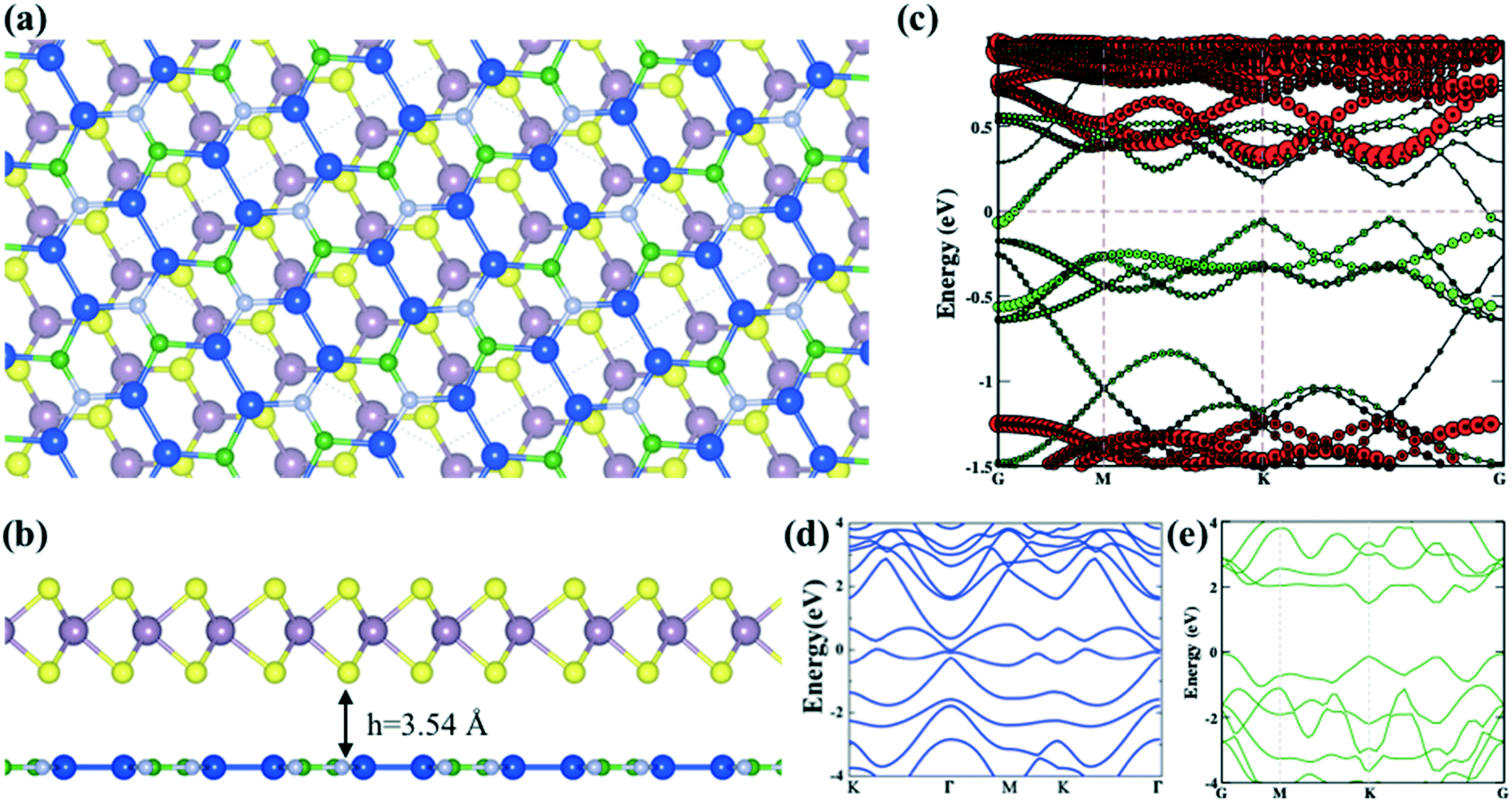 | ||
| Fig. 1 The optimized mMoS2/Si2BN heterostructure viewed from the (a) top and (b) side and the (c) corresponding band structure (green and red colors represent the electronic band lines of Si2BN and MoS2, respectively). The electronic band structures of pristine (d) Si2BN and (e) MoS2 monolayers. | ||
After the optimization of the crystal structure, no structural distortion is found which is very similar to a previously studied graphene/MoS2 interface.59 The vertical distance between the Si2BN and MoS2 monolayers are 2.99 Å and 2.20 Å for mMoS2/Si2BN and rMoS2/Si2BN, respectively and it shows the vdW equilibrium spacing. The S atoms of MoS2 monolayer shows only physisorption interactions. For the thermodynamic stability of the physical interaction between the Si2BN and MoS2 monolayers, we have calculated the adhesion energy as follows:
| Ead = ESi2BN/MoS2 − ESi2BN − EMoS2 | (2) |
To understand the electronic properties of the mMoS2/Si2BN heterostructure, we have calculated the atom-decomposed electronic band structure as presented in Fig. 1(c). For the comparison of the electronic band structure of mMoS2/Si2BN, we have also computed the individual band structures of the Si2BN and MoS2 monolayers as shown in Fig. 1(d) and (e), respectively. From the electronic band structure of heterostructure, we can see that the electronic band lines slightly changes at high symmetry points and opens the direct bandgap at Γ and K points as presented in Fig. 1(c). The computed electronic band structure shows the metallic behavior of the Si2BN monolayer as presented in Fig. 1(d). Additionally, the calculated band structure of the MoS2 monolayer shows a direct bandgap of 1.64 eV from the valence band maximum, and the conduction band minimum is located at the K-point as shown in Fig. 1(e). The value of the theoretical bandgap 1.64 eV is underestimated compared with the experimental bandgap 1.8 eV.61 During the contact of Si2BN with MoS2 monolayer reduced the bandgap 1.43 eV from 1.64 eV and the Fermi level-shifted towards the conduction band minimum side; due to this, it shows n-type behavior. Also, one band line crosses the Fermi level at the Γ point of the Si2BN monolayer and the electronic band lines are separated as compared to the pristine case at the Γ point as shown in Fig. 1(c). Predominantly, the metallic conductivity in the complex system is mediated by the Si2BN surface.
Previous investigations suggested that the stability of the MoS2 nanoribbon is strongly dependent on edge structures in which the sulphur terminated edges (zigzag direction) had the lowest energy configuration.60,62,63 In the present work, we have mounted the MoS2 nanoribbon on the monolayer surface of Si2BN in which the MoS2 nanoribbon has S atoms on one terminal edge and Mo atoms on the other edge as presented in Fig. 2(a). In the case of rMoS2/Si2BN, the lateral separation distance between nanoribbon MoS2 and its periodic images is 15 Å to prevent physical interactions. The fully optimized structural configuration has slight distortion at the nanoribbon edges which is consistent with the previous literature.60,62,63
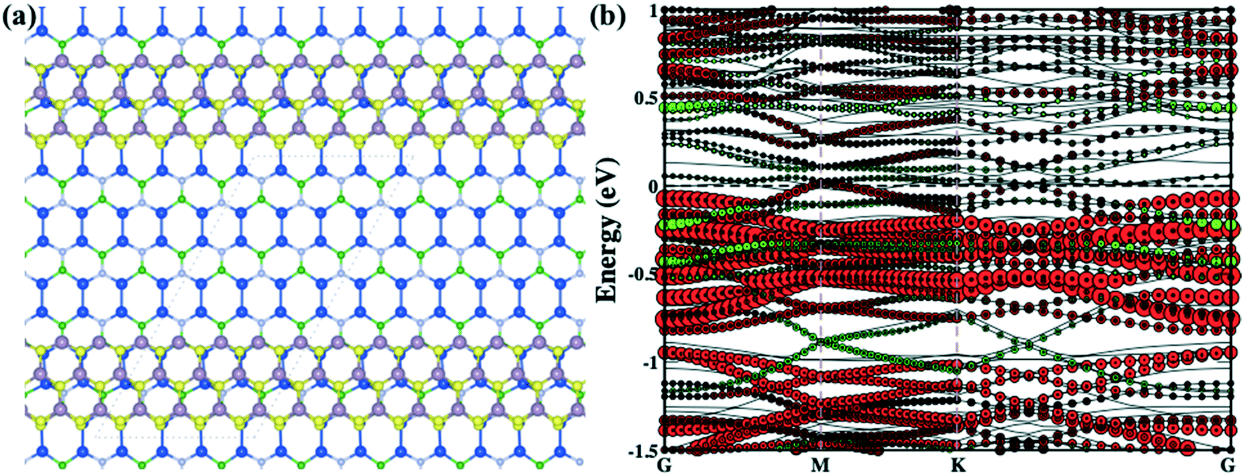 | ||
| Fig. 2 The optimized rMoS2/Si2BN heterostructure (a) and the corresponding band structure (b) (green and red colors represent the electronic band lines of Si2BN and MoS2, respectively). | ||
Furthermore, we have calculated the projected density of states (PDOS) of the pristine Si2BN and MoS2 monolayers as well as the mMoS2/Si2BN and rMoS2/Si2BN heterostructures as shown in Fig. S3.† From the electronic density of states of pristine Si2BN, the monolayer has more contribution from the Si-p orbital and a small contribution comes from the p-orbitals of the B and N atoms at the Fermi level as shown in Fig. S3(a).† Due to the presence of some electronic states at the Fermi level, pristine Si2BN shows metallic behavior. But in the case of the pristine MoS2 monolayer, the electronic states are dominated by the d-orbital of Mo atoms and a very small contribution comes from the S p-orbital near the Fermi level in both the VBM and CBM as presented in Fig. S3(b).† We can see that the pristine MoS2 monolayer shows p-type semiconducting behavior (see Fig. 1e and S3b†). Furthermore, with the interfacial contact between Si2BN and MoS2, the heterostructure (mMoS2/Si2BN) shows metallic behavior in which the p-orbital of Si atoms is responsible for band crossing at the Fermi level. Also, the electronic states of MoS2 shifted towards the CBM side due to the significant vdW interactions between the Si2BN and MoS2 monolayers. According to this, the Si2BN and MoS2 monolayers behave like n-type semiconductors with the contact of the Si2BN surface. There are no significant changes in the electronic states of the Si2BN monolayer because it shows metallic behavior before and after the contact with the MoS2 monolayer. Moreover, during the interfacial contact between a monolayer of Si2BN and MoS2 shows metallic nature for both vdW heterostructure mMoS2/Si2BN and rMoS2/Si2BN. But in this case, the p-orbital of the Si atoms is strongly hybridized with the d-orbital of the Mo atoms, which appears near and at the Fermi level, as shown in Fig. 2(b) and S3(d).† The terminal edge S and Mo atoms of the MoS2 nanoribbon may be a more reactive surface with the Si2BN monolayer and this is why lots of electronic band lines cross the Fermi level in the electronic band structures.
Charge distribution and work function studies
The entirely distinct electronic properties of both mMoS2/Si2BN and rMoS2/Si2BN heterostructures are induced by the different termination of the MoS2 surface, mainly the existence of edge atoms of the MoS2 nanoribbon. The effect of the MoS2 edges is determined by the charge density difference plot. The charge density difference plot is calculated by:| Δρ = ρSi2BN/MoS2 − ρSi2BN − ρMoS2, | (3) |
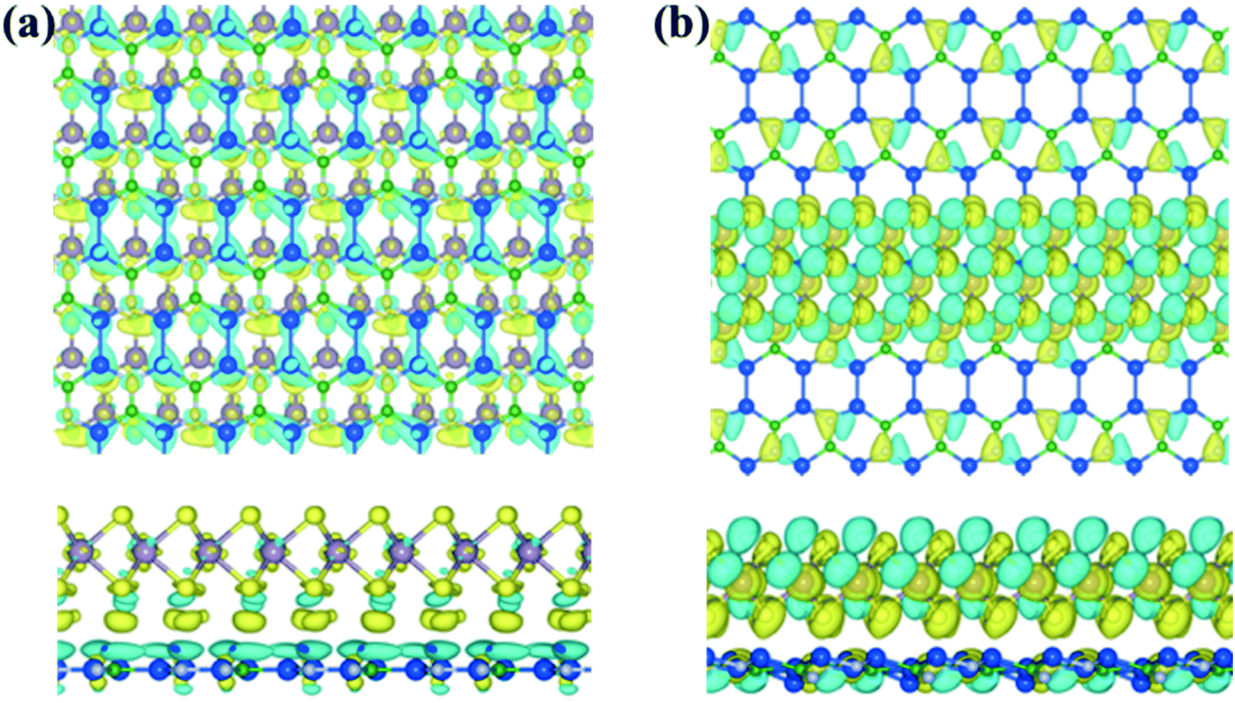 | ||
| Fig. 3 Top view (upper panel) and side view (lower panel) of the electron density difference plots for the (a) mMoS2/Si2BN and (b) rMoS2/Si2BN heterostructures. The iso-value is set as 10−3 e Å−3. The cyan and yellow colors represent the charge depletion and accumulation in space, respectively. | ||
Additionally, we have calculated the planar averaged charge density difference along the z-direction, as shown in Fig. 4(a and b). The positive value on the y-axis indicates electron accumulation and the negative value on the y-axis indicates electron depletion. It is noticed that the electron transfer occurs from the Si2BN monolayer to the MoS2 surface in the heterostructure appearing at the interface region. To quantify the amount of charge transferred, we have used Bader charge analysis for such an interfacial interaction surface. We found that the monolayer Si2BN transfers 0.122 e− and 0.553 e− to the monolayer and nanoribbon MoS2, respectively. This phenomenon can be easily understood by analyzing the electrostatic potential and corresponding simulated work function of the pristine MoS2 and Si2BN monolayers, as presented in Fig. 4(c and d) and 5. The work functions of the pristine MoS2 and Si2BN monolayers are 5.82 eV and 4.32 eV, respectively. However, the mMoS2/Si2BN and rMoS2/Si2BN heterostructures have work functions situated between those of the pristine MoS2 and Si2BN layers. This means that the significant changes in the electrostatic potential regulate the charge redistribution in the heterostructure system. According to that, spontaneous interfacial electron transfer occurs from the Si2BN layer to the MoS2 layer, which is easily justified in terms of the large difference in work functions. It is also known that the electrons transfer from a lower potential region to a higher potential region.68 Due to the significant charge transfer at the interfacial region, an internal electric field is generated which can effectively enhance the photogenerated electron–hole (e−/h+) pair separation between the MoS2 and Si2BN layers. In previous investigations, it was found that a similar charge redistribution occurred in hybrid MoS2/graphene60 and black phosphorus/BiVO4.68
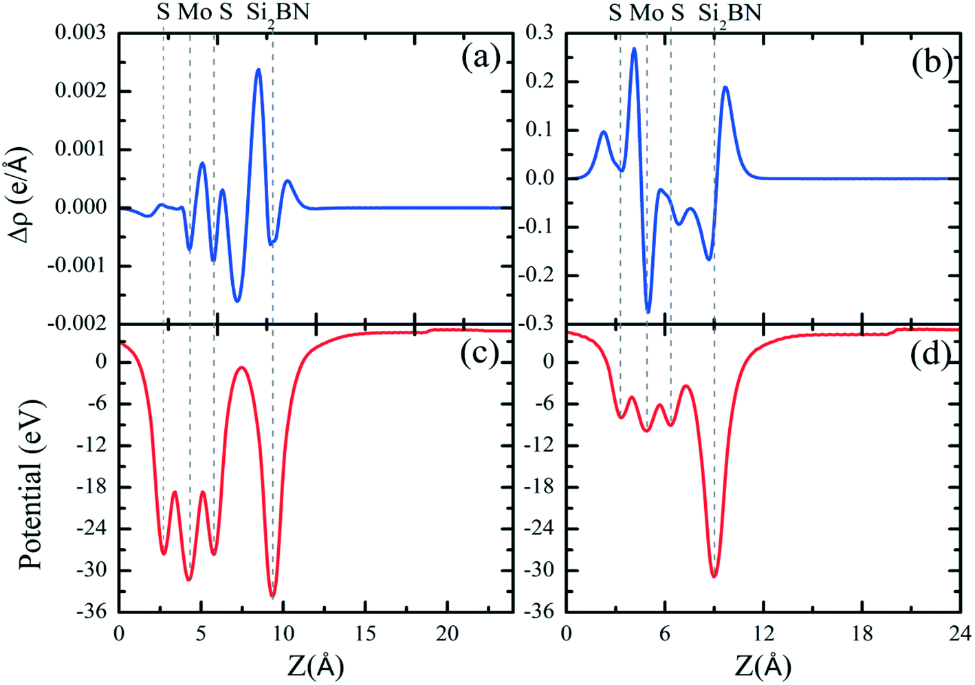 | ||
| Fig. 4 Planar-averaged electron density differences Δρ(z) for the (a) mMoS2/Si2BN and (b) rMoS2/Si2BN heterostructures. The electrostatic potentials for the (c) mMoS2/Si2BN and (d) rMoS2/Si2BN heterostructures. | ||
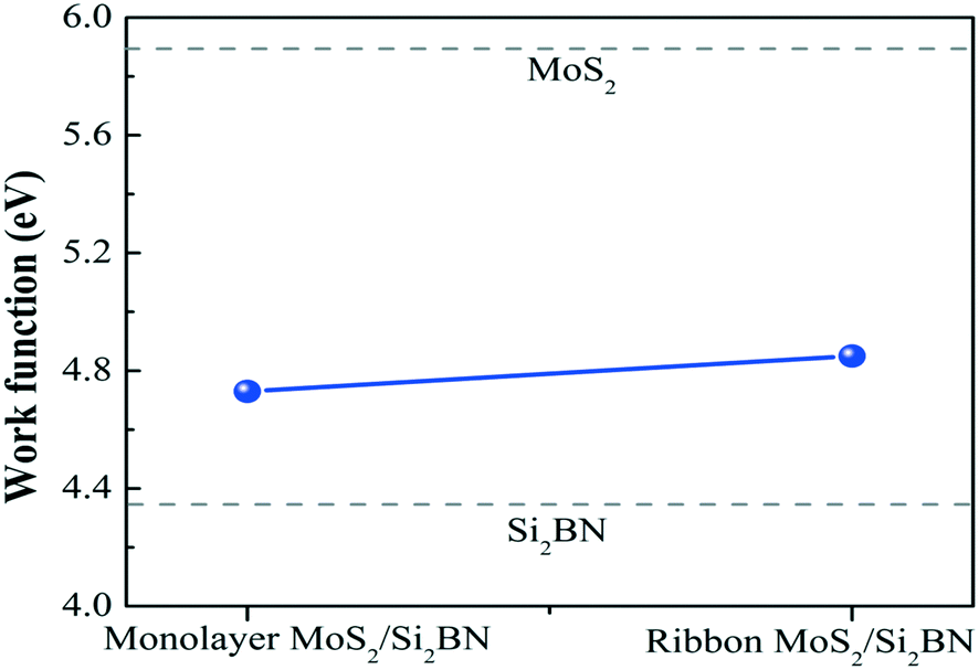 | ||
| Fig. 5 Work functions of mMoS2/Si2BN and rMoS2/Si2BN. The dotted lines for pristine MoS2 and Si2BN are also shown for comparison. | ||
Mechanism of photocatalytic activity
For the purpose of exploring in detail the regioselectivity of hydrogen atoms, the binding characteristics on different sides of both MoS2/Si2BN heterostructures (monolayer and ribbon) were explored in our calculations. Fig. 6(a–d) shows the top and side views of mMoS2/Si2BN and rMoS2/Si2BN with a H-atom adsorbed on either the MoS2-side or Si2BN-side. To get a better understanding of the favorable binding sites on both sides of mMoS2/Si2BN and rMoS2/Si2BN, distinct binding sites were examined. In the case of the Si2BN-side, the sites were located above the B, N, and Si atoms and Si–Si, B–N, N–Si, and Si–Si bridges, and hollow sites. In the case of the MoS2-side, four kinds of binding sites were considered, in which the first one is located above the Mo-atoms, the second is above the S-atoms, the third is between the Mo–S bonds and the last one is at the hollow site of the hexagons that contain 3Mo- and 3S-atoms. The summarized adsorption energies at the most stable binding sites for an H-atom adsorbed on both sides are described in Table 1. It is obvious from this table that the adsorption process of a H-atom on rMoS2/Si2BN is better than that on mMoS2/Si2BN, with the adsorption energy being −0.176 eV in the case of the MoS2-side and −0.285 eV in the case of the Si2BN-side. The thermodynamic stability of the MoS2/Si2BN vdW heterostructure at 300 K was investigated by ab initio molecular dynamics (MD) simulations based on the Nose thermostat algorithm. The evolution of the total potential energy with simulation time and the final snapshot after 10 ps are shown in Fig. S4.† The total energies at 300 K remain almost invariant during the simulation. One can see in Fig. S4† that the final energy fluctuations tend to smoothen in the energy range up to 3 eV for mMoS2/Si2BN and 5 eV for rMoS2/Si2BN. Our results indicate that the honeycomb network of the MoS2 and Si2BN regions remain unchanged which led to a stable structure with no breaking of bonds, basically, under 300 K. MD simulations suggest that the MoS2/Si2BN vdW heterostructure is thermally stable at 300 K.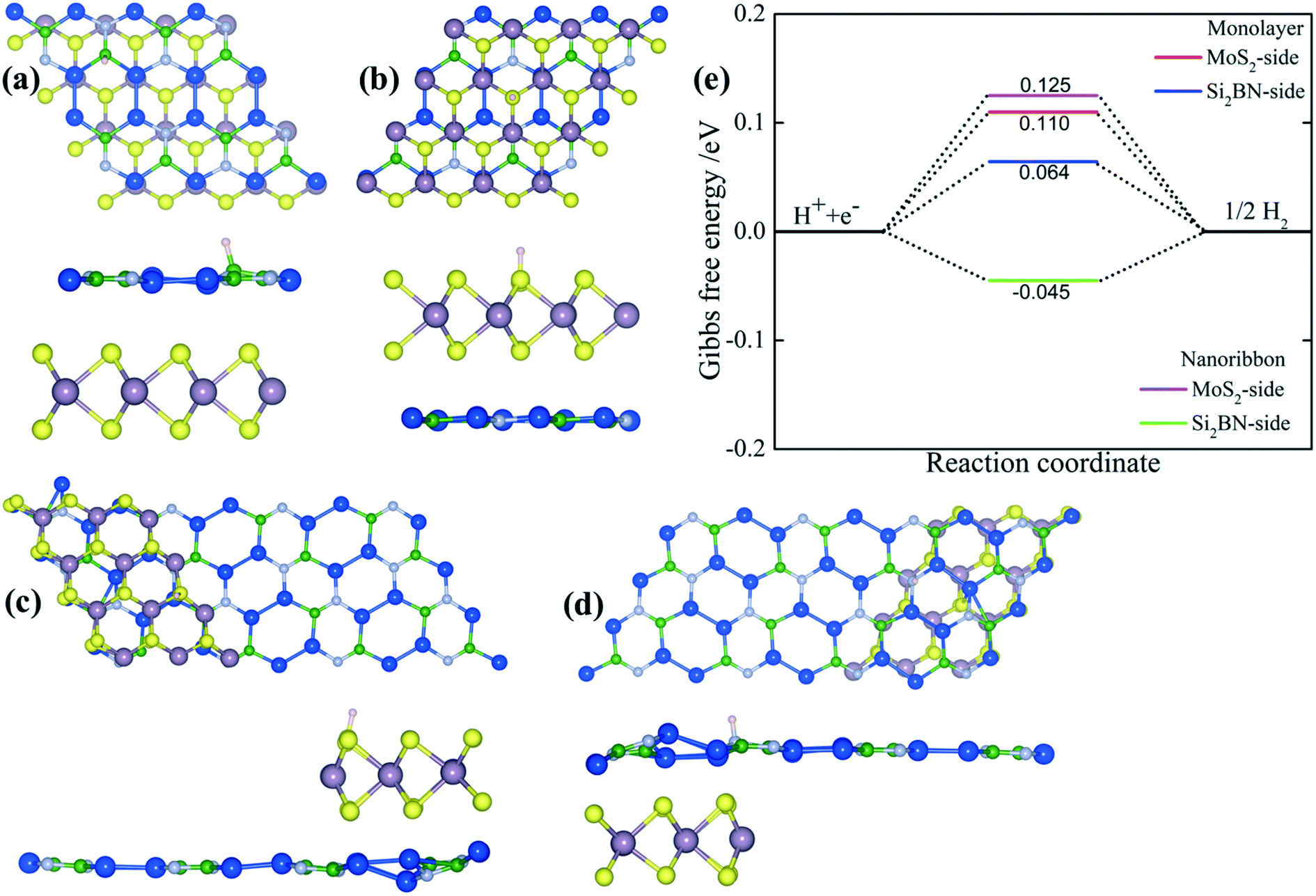 | ||
| Fig. 6 (a–d) Top and side views of monolayer and ribbon MoS2/Si2BN with a hydrogen atom adsorbed at the most favorable site on both sides. (e) Calculated Gibbs free energy profile for the hydrogen evolution reaction (HER) on both sides of monolayer MoS2/Si2BN and ribbon MoS2/Si2BN. | ||
| Systems | E a (eV) | ΔGH* (eV) | Bader analysis | |||
|---|---|---|---|---|---|---|
| MoS2-Side | Si2BN-Side | MoS2-Side | Si2BN-Side | MoS2-Side | Si2BN-Side | |
| Monolayer MoS2 | −0.13 | −0.115 | 0.11 | 0.125 | 0.056 | 0.14 |
| Ribbon MoS2 | −0.176 | −0.285 | 0.064 | −0.045 | 0.062 | 0.99 |
To gain insight into the adsorption mechanisms, the adsorption free energy (ΔGH*) in the different sides of both heterostructures was also calculated, as illustrated in Table 1 and Fig. 6e. Generally, a potential catalyst with a better and efficient HER activity should be characterized by zero adsorption free energy (ΔGH* → 0). It is noted that the adsorption free energies are near zero in the case of rMoS2/Si2BN with about −0.045 eV and −0.062 eV when hydrogen is adsorbed on the MoS2-side and Si2BN-side, respectively, which is better compared to mMoS2/Si2BN with ΔGH*a of about 0.11 eV and 0.125 eV for the MoS2-side and Si2BN-side, respectively. Consequently, the hydrogen evolution reaction activity in the case of ribbon MoS2/Si2BN is ideal compared to that of the monolayer MoS2/Si2BN. As previously reported, the Gibbs free energy on the pristine MoS2 and Si2BN monolayers were found to be 1.29–1.80 eV (ref. 60) and 0.122 eV (ref. 54), respectively.
To further quantify this detail, the charge transfer mechanism was evaluated by Bader charge analysis to consider the distribution of charge when an H-atom is adsorbed on the different sides of the MoS2/Si2BN heterostructures. In the case of a hydrogen atom adsorbed either on the MoS2-side or Si2BN-side of mMoS2/Si2BN, the hydrogen gains a net amount of charge of 0.056 |e| and 0.014 |e|, respectively, and when a hydrogen atom is adsorbed either on the MoS2-side and Si2BN-side of rMoS2/Si2BN, the hydrogen atom gains a charge of 0.062 |e| and 0.99 |e|, respectively, indicating that the charge transfer mechanism arises through the MoS2- and Si2BN-sides of the heterostructures to the H-atom.
Based on the above-mentioned results of work function, Fig. 7 shows the activity of MoS2/Si2BN for photocatalytic water splitting, which is explored by comparing the band positions of MoS2 and Si2BN before and after contact to the reduction and oxidation potentials. The Fermi level of MoS2 before contact is very close to the VB, and that of Si2BN is located near the CB. Furthermore, the Fermi level equilibration leads to the generation of an internal electric field and hence charge diffusion; this, in turn, shifts the band positions of MoS2. Thus, the energy levels of MoS2 shift upward along with the Fermi level, whereas those of Si2BN shift downward along with the Fermi level until the Fermi level of MoS2 and Si2BN reach an equilibrium; this leads to the generation of an internal electric field with a negatively charged portion at the interface of the MoS2 region and a positively charged portion at the interface of the Si2BN region. On the other hand, by definition, the CBM must be situated above the H+/H2 reduction potential (0 V vs. NHE), while the VBM must be located below the O2/H2O oxidation potential (1.23 V vs. NHE). In the case of before contact, the CBM potential of MoS2 is −0.33 eV lower than the reduction potential of H+/H2, while the VBM potential is 0.08 eV higher than the oxidation potential of O2/H2O, which is sufficient for oxidation and reduction of water considering the overpotential factor. After contact, the relative positions of the CBM and VBM of MoS2 will change with the Fermi level due to the charge redistribution. The CBM potential (about −0.84 eV) becomes much lower than the reduction potential of H+/H2, while the VBM potential (0.80 eV) of MoS2 becomes −0.43 eV lower than the oxidation potential of O2/H2O.
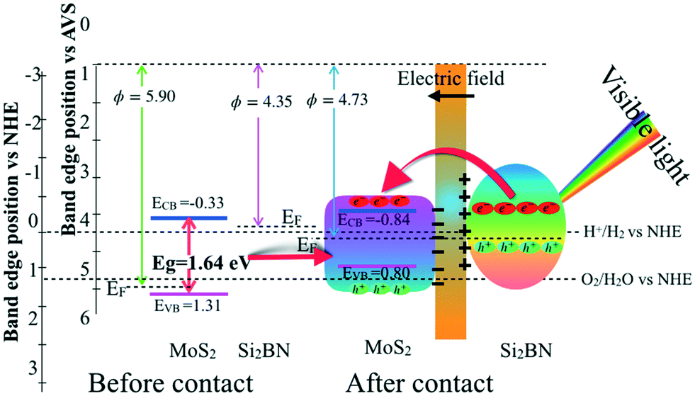 | ||
| Fig. 7 A schematic diagram of the band configuration and the charge separation at the interface of MoS2/Si2BN under visible-light irradiation. | ||
The optical absorption spectra is an important factor in describing the performance of the photocatalyst of vdW heterostructures for photocatalytic activities. Thus, the absorption spectra of the fully optimized pristine MoS2 and Si2BN monolayers, as well as the heterostructures mMoS2/Si2BN and rMoS2/Si2BN, were studied by computing the imaginary component of the complex dielectric function as illustrated in Fig. 8. According to the computed absorption coefficients in the visible light range between 1.55 eV and 3.1 eV, the Si2BN monolayer scarcely absorbs visible light compared to MoS2, which displays a significant absorption capacity. However, in the case of the MoS2/Si2BN heterostructures, the optical absorption of mMoS2/Si2BN is significantly greater compared to that of rMoS2/Si2BN and the Si2BN monolayer but is slightly less than that of the MoS2 monolayer. These indicate the promising application of the mMoS2/Si2BN heterostructure as a great light absorber.
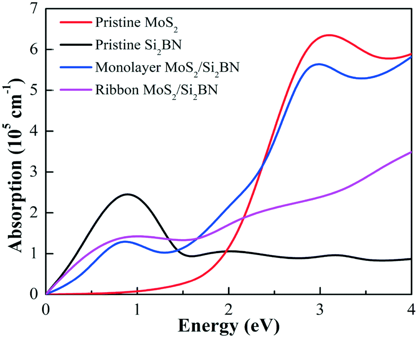 | ||
| Fig. 8 Optical absorption spectra of the pristine MoS2 monolayer, Si2BN monolayer, mMoS2/Si2BN, and rMoS2/Si2BN, represented by red, black, blue, and magenta lines, respectively. | ||
Conclusions
In summary, the effects of MoS2 edge structure on the electronic structures, charge transport, and work functions of MoS2/Si2BN heterostructures have been investigated using first-principles calculations. The interfacial interactions between edge-free MoS2 and a Si2BN monolayer are weak vdW interactions which do not affect the properties of Si2BN and the semiconducting behavior of the MoS2 monolayer; however, the Fermi level is shifted towards the conduction band side (n-type semiconductor conductivity) in the case of the MoS2 monolayer. When MoS2 has exposed edges, the MoS2 ribbon on a Si2BN monolayer in the current study, the binding strength and electronic coupling at the interface are enhanced, resulting in more electrons transferred from the Si2BN surface to the MoS2 nanoribbon surface which can effectively enhance the photogenerated electron–hole pair separation between the MoS2 and Si2BN nanosheets. Additionally, the excess electrons at the MoS2 surface are chemically more active, which can be used for energy storage and gas sensing applications. The electronic properties of MoS2/Si2BN heterostructures is strongly influenced by the MoS2 dimensions, which could be potential materials for nanoelectronic devices and catalytic materials.Conflicts of interest
There are no conflicts to declare.Acknowledgements
The authors thank Olle Engkvists Stiftelse and the Swedish Research Council (VR) for financial support. AA acknowledges the PPR2 project (MISTERSFC-CNRST) for providing financial support. SNIC and HPC2N are acknowledged for providing the computing facilities.References
- K. Xiong, et al. Functional Group Effects on the Photoelectronic Properties of MXene (Sc2CT2, T = O, F, OH) and Their Possible Photocatalytic Activities, Sci. Rep., 2017, 7, 15095 CrossRef PubMed.
- K. Pandey, et al. First step to investigate nature of electronic states and transport in flower-like MoS2: Combining experimental studies with computational calculations, Sci. Rep., 2016, 6, 32690 CrossRef CAS PubMed.
- D. Singh, S. K. Gupta, Y. Sonvane, A. Kumar and R. Ahuja, 2D-HfS 2 as an efficient photocatalyst for water splitting, Catal. Sci. Technol., 2016, 6, 6605–6614 RSC.
- D. Singh, N. Singh, S. K. Gupta and Y. Sonvane, Effect on electronic and optical properties of Frenkel and Schottky defects in HfS2 monolayer, AIP Conf. Proc., 2018, 090023, DOI:10.1063/1.5028938.
- D. Singh and R. Ahuja, Enhanced Optoelectronic and Thermoelectric Properties by Intrinsic Structural Defects in Monolayer HfS 2, ACS Appl. Energy Mater., 2019, 2, 6891–6903 CrossRef CAS.
- B. Radisavljevic, A. Radenovic, J. Brivio, V. Giacometti and A. Kis, Single-layer MoS2 transistors, Nat. Nanotechnol., 2011, 6, 147–150 CrossRef CAS PubMed.
- C. Tsai, F. Abild-Pedersen and J. K. Nørskov, Tuning the MoS 2 Edge-Site Activity for Hydrogen Evolution via Support Interactions, Nano Lett., 2014, 14, 1381–1387 CrossRef CAS PubMed.
- G. Ye, et al. Defects Engineered Monolayer MoS 2 for Improved Hydrogen Evolution Reaction, Nano Lett., 2016, 16, 1097–1103 CrossRef CAS PubMed.
- C.-F. Fu, X. Wu and J. Yang, Material Design for Photocatalytic Water Splitting from a Theoretical Perspective, Adv. Mater., 2018, 30, 1802106 CrossRef PubMed.
- R. K. Biroju, et al. Hydrogen Evolution Reaction Activity of Graphene–MoS 2 van der Waals Heterostructures, ACS Energy Lett., 2017, 2, 1355–1361 CrossRef CAS.
- C. Chowdhury, S. Karmakar and A. Datta, Monolayer Group IV–VI Monochalcogenides: Low-Dimensional Materials for Photocatalytic Water Splitting, J. Phys. Chem. C, 2017, 121, 7615–7624 CrossRef.
- D. Voiry, et al. The role of electronic coupling between substrate and 2D MoS2 nanosheets in electrocatalytic production of hydrogen, Nat. Mater., 2016, 15, 1003–1009 CrossRef CAS PubMed.
- J. Yan, et al. Construction of a 2D Graphene-Like MoS 2 /C 3 N 4 Heterojunction with Enhanced Visible-Light Photocatalytic Activity and Photoelectrochemical Activity, Chem. – Eur. J., 2016, 22, 4764–4773 CrossRef CAS PubMed.
- S. Bawari, T. N. Narayanan and J. Mondal, Atomistic Elucidation of Sorption Processes in Hydrogen Evolution Reaction on a van der Waals Heterostructure, J. Phys. Chem. C, 2018, 122, 10034–10041 CrossRef CAS.
- F. A. Frame and F. E. Osterloh, CdSe-MoS 2 : A Quantum Size-Confined Photocatalyst for Hydrogen Evolution from Water under Visible Light, J. Phys. Chem. C, 2010, 114, 10628–10633 CrossRef CAS.
- Z. Li, X. Meng and Z. Zhang, Recent development on MoS2-based photocatalysis: A review, J. Photochem. Photobiol., C, 2018, 35, 39–55 CrossRef CAS.
- D. Lu, et al. Highly Efficient Visible-Light-Induced Photoactivity of Z-Scheme g-C 3 N 4 /Ag/MoS 2 Ternary Photocatalysts for Organic Pollutant Degradation and Production of Hydrogen, ACS Sustainable Chem. Eng., 2017, 5, 1436–1445 CrossRef CAS.
- E. Parzinger, et al. Photocatalytic Stability of Single- and Few-Layer MoS 2, ACS Nano, 2015, 9, 11302–11309 CrossRef CAS PubMed.
- S. Min and G. Lu, Sites for High Efficient Photocatalytic Hydrogen Evolution on a Limited-Layered MoS 2 Cocatalyst Confined on Graphene Sheets—The Role of Graphene, J. Phys. Chem. C, 2012, 116, 25415–25424 CrossRef CAS.
- W. Gao, M. Wang, C. Ran and L. Li, Facile one-pot synthesis of MoS 2 quantum dots–graphene–TiO 2 composites for highly enhanced photocatalytic properties, Chem. Commun., 2015, 51, 1709–1712 RSC.
- Y.-F. Zhao, et al. Cu 2 O Decorated with Cocatalyst MoS 2 for Solar Hydrogen Production with Enhanced Efficiency under Visible Light, J. Phys. Chem. C, 2014, 118, 14238–14245 CrossRef CAS.
- W. Peng and X. Li, Synthesis of MoS2/g-C3N4 as a solar light-responsive photocatalyst for organic degradation, Catal. Commun., 2014, 49, 63–67 CrossRef CAS.
- K. F. Mak, C. Lee, J. Hone, J. Shan and T. F. Heinz, Atomically Thin <math display="inline"> <msub> <mi>MoS</mi> <mn>2</mn> </msub> </math> : A New Direct-Gap Semiconductor, Phys. Rev. Lett., 2010, 105, 136805 CrossRef PubMed.
- P. Joensen, R. F. Frindt and S. R. Morrison, Single-layer MoS2, Mater. Res. Bull., 1986, 21, 457–461 CrossRef CAS.
- A. N. Andriotis, E. Richter and M. Menon, Prediction of a new graphenelike <math> <mrow> <msub> <mi>Si</mi> <mn>2</mn> </msub> <mi>BN</mi> </mrow> </math> solid, Phys. Rev. B, 2016, 93, 081413 CrossRef.
- C. Jin, et al. Ultrafast dynamics in van der Waals heterostructures, Nat. Nanotechnol., 2018, 13, 994–1003 CrossRef CAS PubMed.
- W. Yang, et al. Interlayer interactions in 2D WS 2 /MoS 2 heterostructures monolithically grown by in situ physical vapor deposition, Nanoscale, 2018, 10, 22927–22936 RSC.
- M. Zhao, et al. Interlayer coupling in anisotropic/isotropic van der Waals heterostructures of ReS2 and MoS2 monolayers, Nano Res., 2016, 9, 3772–3780 CrossRef CAS.
- S. Wang, X. Wang and J. H. Warner, All Chemical Vapor Deposition Growth of MoS 2 :h-BN Vertical van der Waals Heterostructures, ACS Nano, 2015, 9, 5246–5254 CrossRef CAS PubMed.
- X. Zhou, et al. Vertical heterostructures based on SnSe 2 /MoS 2 for high performance photodetectors, 2D Mater., 2017, 4, 025048 CrossRef.
- F. Wang, et al. Tuning Coupling Behavior of Stacked Heterostructures Based on MoS2, WS2, and WSe2, Sci. Rep., 2017, 7, 44712 CrossRef CAS PubMed.
- Z. Huang, et al. Band structure engineering of monolayer MoS 2 on h-BN: first-principles calculations, J. Phys. D: Appl. Phys., 2014, 47, 075301 CrossRef.
- Y. P. Venkata Subbaiah, K. J. Saji and A. Tiwari, Atomically Thin MoS 2 : A Versatile Nongraphene 2D Material, Adv. Funct. Mater., 2016, 26, 2046–2069 CrossRef CAS.
- J.-W. Jiang, Graphene versus MoS2: A short review, Front. Phys., 2015, 10, 287–302 CrossRef.
- S. Bertolazzi, D. Krasnozhon and A. Kis, Nonvolatile Memory Cells Based on MoS 2 /Graphene Heterostructures, ACS Nano, 2013, 7, 3246–3252 CrossRef CAS PubMed.
- W. Zhou, et al. Synthesis of Few-Layer MoS 2 Nanosheet-Coated TiO 2 Nanobelt Heterostructures for Enhanced Photocatalytic Activities, Small, 2013, 9, 140–147 CrossRef CAS PubMed.
- Y. Li, C.-Y. Xu, J.-Y. Wang and L. Zhen, Photodiode-Like Behavior and Excellent Photoresponse of Vertical Si/Monolayer MoS2 Heterostructures, Sci. Rep., 2015, 4, 7186 CrossRef PubMed.
- H. Fang, et al. Strong interlayer coupling in van der Waals heterostructures built from single-layer chalcogenides, Proc. Natl. Acad. Sci. U. S. A., 2014, 111, 6198–6202 CrossRef CAS PubMed.
- M.-H. Chiu, et al., Determination of band alignment in the single-layer MoS2/WSe2 heterojunction, Nat. Commun., 2015, 6, 7666 CrossRef CAS PubMed.
- D. Singh, S. K. Gupta, Y. Sonvane, T. Hussain and R. Ahuja, Achieving ultrahigh carrier mobilities and opening the band gap in two-dimensional Si 2 BN, Phys. Chem. Chem. Phys., 2018, 20, 21716–21723 RSC.
- K. S. Novoselov, A. Mishchenko, A. Carvalho and A. H. Castro Neto, 2D materials and van der Waals heterostructures, Science, 2016, 353, aac9439 CrossRef CAS PubMed.
- P. Blanchard and E. Brüning, Density Functional Theory of Atoms and Molecules, in Progress in Mathematical Physics, 2015, pp. 563–573, DOI:10.1007/978-3-319-14045-2_37.
- L. J. Bartolotti and K. Flurchick, An Introduction to Density Functional Theory, in Reviews in Computational Chemistry, 2007, pp. 187–216, DOI:10.1002/9780470125847.ch4.
- G. Kresse and J. Furthmüller, Efficient iterative schemes for ab initio total-energy calculations using a plane-wave basis set, Phys. Rev. B: Condens. Matter Mater. Phys., 1996, 54, 11169–11186 CrossRef CAS PubMed.
- W. Kohn, Density Functional and Density Matrix Method Scaling Linearly with the Number of Atoms, Phys. Rev. Lett., 1996, 76, 3168–3171 CrossRef CAS PubMed.
- P. Hohenberg and W. Kohn, Inhomogeneous Electron Gas, Phys. Rev., 1964, 136, B864–B871 CrossRef.
- J. P. Perdew, K. Burke and M. Ernzerhof, Generalized Gradient Approximation Made Simple, Phys. Rev. Lett., 1996, 77, 3865–3868 CrossRef CAS PubMed.
- W. Kohn and L. J. Sham, Self-Consistent Equations Including Exchange and Correlation Effects, Phys. Rev., 1965, 140, A1133–A1138 CrossRef.
- G. Kresse and D. Joubert, From ultrasoft pseudopotentials to the projector augmented-wave method, Phys. Rev. B: Condens. Matter Mater. Phys., 1999, 59, 1758–1775 CrossRef CAS.
- S. Grimme, J. Antony, S. Ehrlich and H. Krieg, A consistent and accurate ab initio parametrization of density functional dispersion correction (DFT-D) for the 94 elements H-Pu, J. Chem. Phys., 2010, 132, 154104 CrossRef PubMed.
- H. J. Monkhorst and J. D. Pack, Special points for Brillouin-zone integrations, Phys. Rev. B: Solid State, 1976, 13, 5188–5192 CrossRef.
- M. Yu and D. R. Trinkle, Accurate and efficient algorithm for Bader charge integration, J. Chem. Phys., 2011, 134, 064111 CrossRef PubMed.
- D. Singh, S. K. Gupta, Y. Sonvane and I. Lukačević, Antimonene: a monolayer material for ultraviolet optical nanodevices, J. Mater. Chem. C, 2016, 4, 6386–6390 RSC.
- D. Singh, S. Chakraborty and R. Ahuja, Emergence of Si 2 BN Monolayer as Efficient HER Catalyst under Co-functionalization Influence, ACS Appl. Energy Mater., 2019, 2, 8441–8448 CrossRef CAS.
- H. R. Mahida, et al. The influence of edge structure on the optoelectronic properties of Si 2 BN quantum dot, J. Appl. Phys., 2019, 126, 233104 CrossRef.
- A. N. Andriotis, E. Richter and M. Menon, Prediction of a new graphenelike Si2BN solid, Phys. Rev. B, 2016, 93, 2–4 CrossRef.
- V. Shukla, R. B. Araujo, N. K. Jena and R. Ahuja, The curious case of two dimensional Si2BN: A high-capacity battery anode material, Nano Energy, 2017, 41, 251–260 CrossRef CAS.
- D. Singh, S. K. Gupta, Y. Sonvane and R. Ahuja, High performance material for hydrogen storage: Graphenelike Si2BN solid, Int. J. Hydrogen Energy, 2017, 42, 22942–22952 CrossRef CAS.
- K. Chang, et al., MoS 2 /Graphene Cocatalyst for Efficient Photocatalytic H 2 Evolution under Visible Light Irradiation, ACS Nano, 2014, 8, 7078–7087 CrossRef CAS PubMed.
- M. Guo, et al., Edge dominated electronic properties of MoS 2 /graphene hybrid 2D materials: edge state, electron coupling and work function, J. Mater. Chem. C, 2017, 5, 4845–4851 RSC.
- K. F. Mak, C. Lee, J. Hone, J. Shan and T. F. Heinz, Atomically Thin <math display="inline"> <msub> <mi>MoS</mi> <mn>2</mn> </msub> </math> : A New Direct-Gap Semiconductor, Phys. Rev. Lett., 2010, 105, 136805 CrossRef PubMed.
- W. Li, M. Guo, G. Zhang and Y.-W. Zhang, Edge-Specific Au/Ag Functionalization-Induced Conductive Paths in Armchair MoS 2 Nanoribbons, Chem. Mater., 2014, 26, 5625–5631 CrossRef CAS.
- H. Pan and Y.-W. Zhang, Edge-dependent structural, electronic and magnetic properties of MoS2 nanoribbons, J. Mater. Chem., 2012, 22, 7280 RSC.
- Y. Li, et al. MoS 2 Nanoparticles Grown on Graphene: An Advanced Catalyst for the Hydrogen Evolution Reaction, J. Am. Chem. Soc., 2011, 133, 7296–7299 CrossRef CAS PubMed.
- X. Li, L. Zhang, X. Zang, X. Li and H. Zhu, Photo-Promoted Platinum Nanoparticles Decorated MoS 2 @Graphene Woven Fabric Catalyst for Efficient Hydrogen Generation, ACS Appl. Mater. Interfaces, 2016, 8, 10866–10873 CrossRef CAS PubMed.
- Q. Xiang, J. Yu and M. Jaroniec, Synergetic Effect of MoS 2 and Graphene as Cocatalysts for Enhanced Photocatalytic H 2 Production Activity of TiO 2 Nanoparticles, J. Am. Chem. Soc., 2012, 134, 6575–6578 CrossRef CAS PubMed.
- L. David, R. Bhandavat and G. Singh, MoS 2 /Graphene Composite Paper for Sodium-Ion Battery Electrodes, ACS Nano, 2014, 8, 1759–1770 CrossRef CAS PubMed.
- Y. Chen, et al. Insights into the mechanism of the enhanced visible-light photocatalytic activity of black phosphorus/BiVO 4 heterostructure: a first-principles study, J. Mater. Chem. A, 2018, 6, 19167–19175 RSC.
Footnote |
| † Electronic supplementary information (ESI) available. See DOI: 10.1039/d0cy00420k |
| This journal is © The Royal Society of Chemistry 2020 |