
 Open Access Article
 This Open Access Article is licensed under a Creative Commons Attribution-Non Commercial 3.0 Unported Licence
Topological two-dimensional polymers†
Maximilian A.
Springer‡
 ab,
Tsai-Jung
Liu‡
b,
Agnieszka
Kuc
a and
Thomas
Heine
*abc
ab,
Tsai-Jung
Liu‡
b,
Agnieszka
Kuc
a and
Thomas
Heine
*abc
aHelmholtz-Zentrum Dresden-Rossendorf, Institute of Resource Ecology, Permoserstrasse 15, 04318 Leipzig, Germany. E-mail: thomas.heine@tu-dresden.de
bFaculty for Chemistry and Food Chemistry, TU Dresden, Bergstrasse 66c, 01069 Dresden, Germany
cDepartment of Chemistry, Yonsei University, Seodaemun-gu, Seoul 120-749, Republic of Korea
First published on 24th March 2020
Abstract
There are more than 200 two-dimensional (2D) networks with different topologies. The structural topology of a 2D network defines its electronic structure. Including the electronic topological properties, it gives rise to Dirac cones, topological flat bands and topological insulators. In this Tutorial Review, we show how electronic properties of 2D networks can be calculated by means of a tight-binding approach, and how these properties change when 2nd-neighbour interactions and spin–orbit coupling are included. We explain how to determine whether or not the resulting electronic features have topological signatures by calculation of Chern numbers, Z2 invariants, and by the nanoribbon approach. This tutorial gives suggestions how such topological properties could be realized in explicit atomistic chemical 2D systems made of molecular frameworks, in particular in 2D polymers, where the edges and vertices of a given 2D net are substituted by properly selected molecular building blocks and stitched together in such a way that long-range π-conjugation is retained.
 Maximilian A. Springer | Maximilian A. Springer received his BSc (2015) and MSc (2018) in Chemistry from Leipzig University, Germany. During his studies, he accomplished research stays at Memorial University of Newfoundland, St. John's, Canada (2015) and Monash University, Melbourne, Australia (2016). He pursues his PhD studies under supervision of Thomas Heine and Agnieszka Kuc at the Leipzig research site of Helmholtz-Zentrum Dresden-Rossendorf, Institute of Resource Ecology and TU Dresden. His current research focuses on the relation of electronic structure and topology in 2D polymers. |
 Tsai-Jung Liu | Tsai-Jung Liu received her BSc (2016) and MSc (2018) in Chemistry from National Taiwan University (NTU), Taiwan. Afterwards, she worked as a research assistant at NTU. Since 2019, she is pursuing her PhD under the supervision of Thomas Heine and Agnieszka Kuc at Technical University Dresden, Germany. Her current research mainly focuses on the electronic structures and topological properties of 2D polymers. |
 Agnieszka Kuc | Agnieszka Kuc graduated from Wroclaw University in 2003 with MSc in Physical Chemistry. She completed her PhD in Chemistry under the supervision of Prof. Gotthard Seifert at TU Dresden in 2008. She habilitated in Physics in 2018 under mentoring of Prof. Thomas Heine at Jacobs University Bremen. She is currently working as group leader at Helmholtz-Zentrum Dresden-Rossendorf. Her research interests include, amongst others, electronic structure simulations and vibrational properties of 2D inorganic and hybrid materials, such as transition-metal dichalcogenides, conjugated polymers, metal- and covalent organic frameworks, perovskites. |
 Thomas Heine | Thomas Heine graduated in physics from TU Dresden under the guidance of Gotthard Seifert. After various research stages he obtained the venia legendi in Physical Chemistry at TU Dresden. In 2008, he was appointed as Associate Professor of Theoretical Physics at Jacobs University, and moved as Professor of Theoretical Chemistry to Leipzig University in 2015. Since 2018 he holds the Chair of Theoretical Chemistry at TU Dresden and leads the Theoretical Chemistry group at the Leipzig branch of Helmholtz-Zentrum Dresden-Rossendorf. His research interests include framework materials, two-dimensional crystals, theoretical spectroscopy, and method development for theoretical materials science. |
Key learning points(1) The variety of 2D networks, their structural topology, characteristics, classification, and nomenclature.(2) The impact of the networks on the electronic properties and topological signatures. (3) Tight-binding approach to band structure representation of 2D nets, including its extension to 2nd-neighbour interaction, spin–orbit coupling, and calculation of electronic topological properties using Chern numbers, Z2 invariants and nanoribbon approach. (4) Realization of 2D nets in 2D polymers, the importance of building blocks, π-conjugation, and molecular connectivity. (5) Building blocks design towards topological 2D polymers with signatures of corresponding 2D nets. |
1 Introduction
The creation of materials with ever-new functionalities is a core target of chemistry, where different means to achieve functionalities are utilized in its various disciplines. For example, in organic and metal–organic chemistry, these are functional groups. They, in interplay with the molecular structure and other features, such as aromaticity, are the principal determinant for intermolecular interactions, and, thus, control reactivity, selectivity and catalytic performance. In inorganic chemistry and solid-state physics, functionality is given both by the elemental composition of the material and by the arrangement of the material's atoms in a network. This is evident for materials that possess polytypes, which can show strongly different properties and functionalities. Striking examples include insulating diamond vs. conducting graphite; grey, brittle α vs. metallic, ductile β tin; or the three polytypes of single-layer MoS2: semiconducting 2H, metallic 1T, and topological 1T′. The different properties and functionalities in these polytypes arise from the impact of the network connectivities (coordination) on the electronic system, where the frontier electrons determine the material's properties. Apart from electronic properties, there are other network-imposed properties, such as crack propagation, lubrication, or mechanical properties.1Framework materials with sufficient crystallinity, in particular covalent-organic frameworks (COFs)2–4 and conjugated two-dimensional (2D) polymers,5–7 offer to combine both molecular and network-imposed functionalities. Both terms, 2D COFs and 2D polymers, emerge from different communities and are used in a rather non-intuitive way. 2D COFs typically refer to layered materials, to date usually lacking a long-range crystalline order. On the other hand, the long-range order is required for 2D polymers.8 To date, however, most reports on framework materials focus on the molecular functionality, while the potential of network functionality remains to be exploited. While the network provides mechanical stability and porosity, it has little influence on the electronic structure of most framework materials. This is even true for the quasi-2D systems, which we will focus on in this review.
The potentially high impact of the network topology on the electronic properties has been pointed out in a few recent publications, all of them focusing on 2D systems. 2D polymers with conjugated electronic systems5,9–11 are typically semiconductors and they can possess high charge-carrier mobility. The network topology can impose intriguing electronic structures, including Dirac points or flat bands.12–16 However, while some 2D polymers with, for example, kagome (kgm) and honeycomb (hcb) lattice have been reported, non-trivial electronic topologies have not yet been demonstrated in experiments to date.
One of the obstacles is the degree of crystallinity, which is needed to manifest the lattice-dependent electronic properties. 2D polymers typically are subject to small crystal sizes and high defect densities. However, new synthetic approaches for 2D polymers and 2D COFs allow for flake sizes of up to several microns and with low defect densities.17,18
Even if a highly crystalline framework is available, it is necessary to shift the Fermi level such that it matches the location of the topological feature (e.g., the flat band or the Dirac point). This can be achieved, to some degree, by external means, such as gating by an electrode or an ionic liquid, but it is better controlled by functionalization of the monomers.12
The goal of this Tutorial Review is to provide a scientific background and a theoretical toolbox that is needed for the rational design of 2D polymeric frameworks with network-imposed properties, including topological ones. For this purpose, in the 2nd section, we will give a short introduction on the large variety of suitable 2D nets and their structural features. In the 3rd section, a tight-binding (TB) approach that predicts the network-imposed features of the electronic band structure will be introduced (together with a technical tutorial given in ESI†). This TB model is the principal tool to address the relation between network and electronic structure, and it also characterizes topological states. In Section 4, we will discuss how the electronic structure can be manipulated on the network basis by changing the interaction strength between the lattice points and by changing the chemical potential of the building blocks. In the 5th section, we will provide a map of building blocks that are suitable to form various 2D networks, and a short summary of 2D polymers that have been reported in the literature to date, both computationally and experimentally. Finally, we will provide our personal view on the future of the emerging field of topological 2D polymers in Section 6.
2 2D networks and their structural characterization
The topologies of 2D framework materials can be described by the means of tessellations. These are periodic arrangements of polygons on a flat surface without overlaps or gaps. Vertices are points where more than two polygons meet. Possible tessellations can be categorized by the number and kind of vertices and polygons being used in the tiling.19 It is possible both to construct flat networks by using regular polygons only or to also use irregular polygons. Regular polygons are such that are both equiangular and equilateral. For the purpose of being used in reticular chemistry, the Reticular Chemistry Structural Resource (RCSR) was built.20 It contains 200 2D nets, each labelled with a letter code, which will be used herein. There are four groups of nets that use only regular polygons. The first group is called regular nets (also known as Platonic nets, see Table S1 in ESI†) and contains just one type of vertex and one type of regular polygon: the hexagonal net (hxl, triangles), the square net (sql, squares), and the honeycomb net (hcb, hexagons), see Fig. 1. Since they only contain one type of vertex and one type of polygon (face) they are both face- and vertex-transitive. Nets are usually described by the Schläfli symbols of their vertices, which specify the number and order of polygons meeting at that point. For example, at each vertex in the hcb net (Fig. 1a), the corners of three hexagons meet and, therefore, the net is described by the symbol 63. Semiregular nets are formed by one vertex type and faces of more than one type. These eight nets, being vertex-, but not face-transitive, are cem, fes, fsz, fxt, hca, htb, kgm, and tts (see Table S2, ESI†). They are usually referred to as Archimedean nets, whereas all the vertex-transitive nets together are called Kepler nets or Kepler–Shubnikov nets.21 As it can be seen in Fig. 1d, the kagome net (kgm) is formed by both triangles and hexagons. At each vertex, two hexagons and two triangles meet. Since the hexagons and triangles surround the vertex in an alternate fashion, the Schläfli symbol for this vertex is 3.6.3.6. The third important group of nets with regular polygons are the 20 nets that include exactly two types of vertices – the so-called demiregular nets (see Table S3, ESI†). One example is the krb net, which is formed by two types of faces: hexagons and triangles. At one of the vertices (in Fig. 1e depicted by filled circles), six triangles meet. Therefore, the Schläfli symbol is 36. At the other vertex (unfilled circle, Schläfli symbol 34.6), one hexagon and four triangles meet together. Nets containing irregular polygons mostly include irregular pentagons, e.g., the so-called Cairo tiling mcm. This net can also serve as an example to introduce the concept of duality: a dual net is formed by replacing faces with new vertices at their centre points. The Cairo tiling, which is shown in Fig. 2a, is an example of such a net, since it is a dual to the tts net. According to the nomenclature introduced by O’Keeffe and co-workers,20 it could, therefore, also be called tts-d, with the -d indicating the duality relation. Besides these fundamental tilings, a superstructure of the sql net, the Lieb lattice, recently attracted much attention.22,23 Compared with the sql net, it has one additional centre in the middle of the square's edge (cf.Fig. 1f). In Tables S1–S4 (ESI†), sketches of total of 101 topologies, all of them included in the RCSR database, can be found. They are accompanied by their TB band structures, both for the fundamental net (with only 1st-neighbour interactions), and with the chemically more realistic TB model where both the 1st- and 2nd-neighbour interactions are taken into account. Additionally, spin–orbit coupling was considered. For some of the nets containing irregular polygons, the arrangements of vertices correspond to the hxl net. However, some of the vertices are not connected to all of their neighbours, which gives rise to the irregular polygons in these nets (see Fig. 2b for two representative examples). Due to this complexity, they are assumed to be rather unlikely to be realized in 2D polymers. Therefore, only the tilings with regular polygons and few selected nets with irregular polygons are included in this work.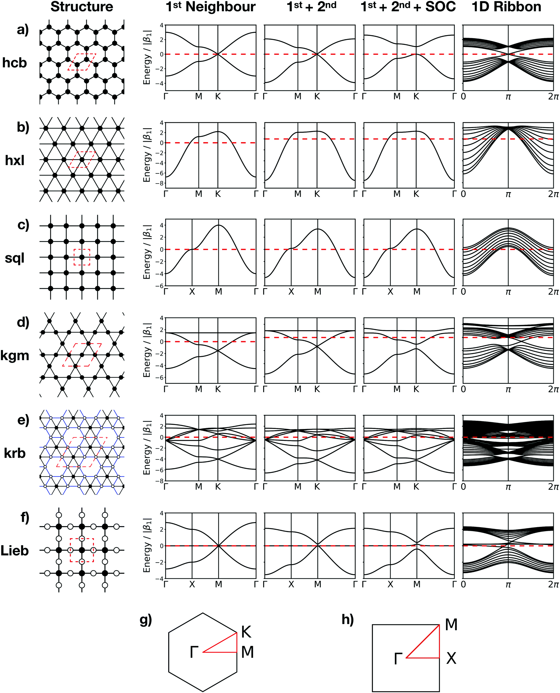 | ||
| Fig. 1 Sketches and band structures are shown for the regular hcb (a), hxl (b), and sql nets (c), the semiregular kgm net (d), the demiregular krb net (e), and the Lieb lattice (f). In the network sketch (column 1), the inequivalent vertices are indicated by filled and empty circles, whereas blue edges in krb indicate that these connections are inequivalent to the black ones. The red dashed lines indicate the unit cells. (Column 2–5) Band structures calculated taking into account (from left to right) only 1st-neighbour interactions, 1st- and 2nd-neighbour interactions, 1st- and 2nd-neighbour interactions with spin–orbit coupling (SOC), and the band structure for 1D ribbons. The energies are given in units of the 1st-neighbour hopping |β1| (see Section 3). (g and h) The first Brillouin zones with the high-symmetry points for the nets with hexagonal and square symmetries. | ||
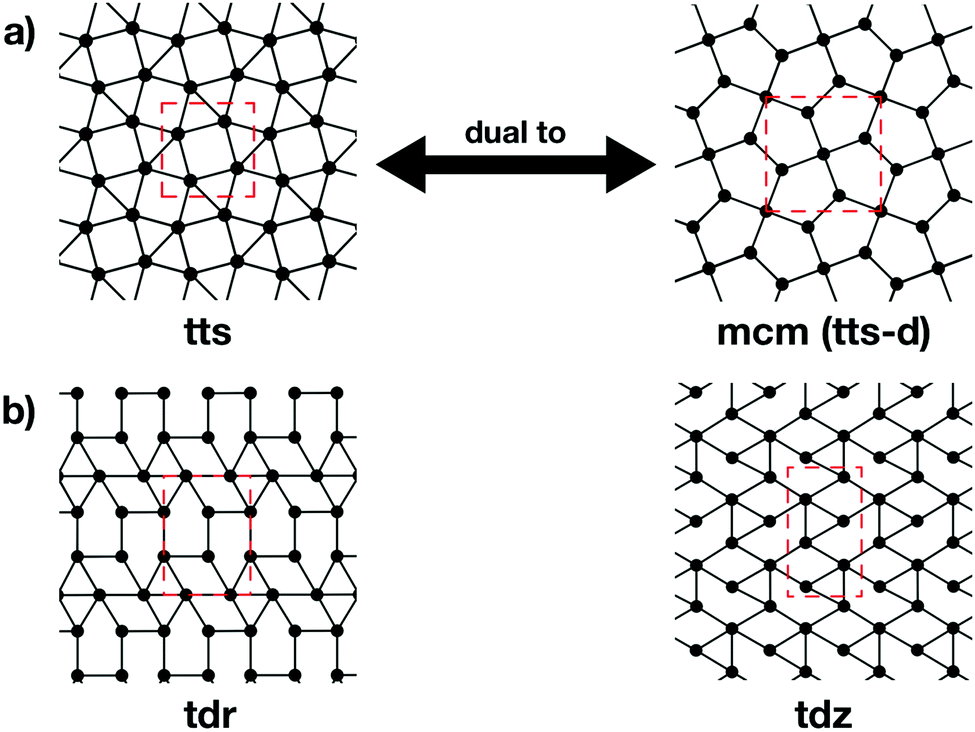 | ||
| Fig. 2 (a) A dual net for a given topology can be obtained by putting vertices at the centres of faces and removing the old vertices. The mcm net is dual to the tts net (and, therefore, also called tts-d), since it can be obtained by putting vertices in the centres of the squares and triangles in the tts net. Vice versa, the tts net is dual to the mcm net and can be obtained by placing vertices in the centres of the irregular pentagons in mcm. Since mcm is formed by irregular polygons, it is an example for irregular nets. (b) Two examples of irregular nets with identical geometric structure to other nets, but with missing links. Such examples are excluded from this investigation. | ||
3 Network-imposed electronic structure
3.1 Impact of network connectivity on the electronic structure
In this section, we will demonstrate how the network connectivity determines significant features of the electronic structure. For demonstration purposes, we discuss two related Platonic nets, namely the hxl and hcb nets, as presented in Fig. 1. We further assume one electron per vertex, that is, exactly half of the electronic states in the band structure are occupied.The hxl lattice has a triangular structure, in which each vertex coordinates with six neighbours. All vertices in hxl are equivalent, hence the corresponding band structure contains only one band, which must be half-filled and, thus, forces the hxl net to be metallic. The hcb net, on the other hand, consists of regular hexagons, in which each vertex connects with three neighbours. It has two sites (identical, but with different environment) in the unit cell, resulting in two bands, which intersect only at the high symmetry K point, forming the so-called Dirac point. Since the band is half filled, the Fermi level (EF) is located exactly at the Dirac point, where, in the non-relativistic limit, massless fermions emerge. They result in exceptionally high charge carrier transport.
From the differences between the hxl and hcb nets, we see that the network connectivities are determinant for forming the electronic structures. The simplest form to translate the network connectivities to a model Schrödinger equation is the TB model. We assume a conjugated π-electron system that is formed by one effective pz orbital per vertex. The linear combination of atomic orbitals (LCAO) ansatz is made exclusively with these pz orbitals (equivalent to Hückel theory for aromatic molecules24), and first we consider only 1st-neighbour interactions (see Fig. 3).
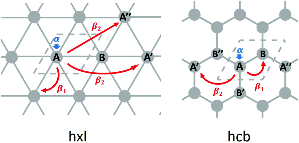 | ||
| Fig. 3 Illustration of the TB parameters: onsite energy α, 1st-neighbour hopping integral β1, and 2nd-neighbour hopping integral β2, for the hxl and hcb nets. The unit cells are indicated with dashed lines. | ||
Equivalent to the Hückel theory, within the simplest TB approximation, each vertex contributes an onsite energy α (typically set to zero) and each 1st-neighbour interaction a hopping contribution β1 (typically set to −1 in order to give energies in units of |β1|, see Fig. 3).
For the hxl net, which only has one vertex per unit cell, the Hamiltonian is given by the expression 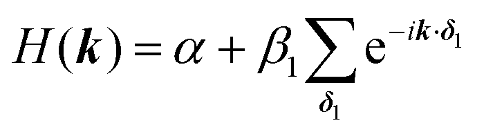 with wave vector k, and δ1 being the vector connecting vertices to their 1st neighbours. In hcb, this is the connection between vertex A with its neighbours B, B′, and B′′ (Fig. 3). For nets with n vertices, it will become a n × n matrix:

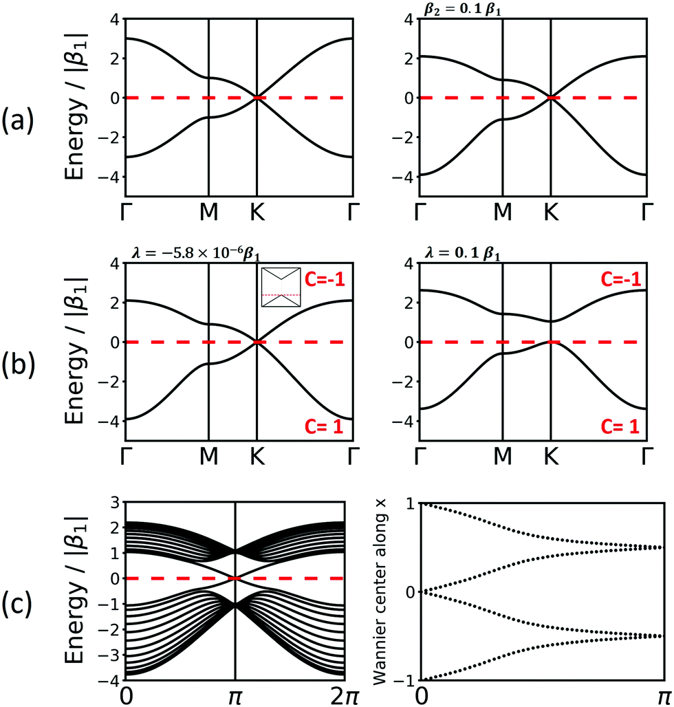 | ||
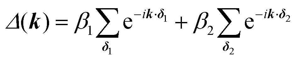
| Fig. 4 Band structure of hcb net considering (a) only 1st-neighbour interactions (left) and also the 2nd-neighbour interactions (right); (b) adding SOC, with λ = −5.8 × 10⁻⁶β1,24 the value for graphene (left), and λ = 0.1β1 (right). The inset in the left figure magnifies the band structure at the K point and shows the tiny gap opening at the Dirac point. (c) Band structure of hcb nanoribbon with 12 units in the width and the Wannier charge centre (WCC) evolution for hcb net. Here, we use an exaggerated value of λ = 0.1β1 to make the effect significant for demonstration. | ||
The first extension of the TB model is to include 2nd-neighbour (and possibly higher) interactions. For the hxl lattice, the geometric distance and the topological distance to 2nd neighbours differ (2nd neighbours are all vertices that are 2 links away): both A′ and A′′ in Fig. 3 are 2nd neighbours of A, but they have a different geometric distance. Here, we treat all topological 2nd neighbours on equal footing, and arbitrarily choose a value of β2 = 0.1β1, which is rather large and therefore somewhat magnifies the impact of 2nd-neighbour interactions on the band structure. The inclusion of 2nd-neighbour interactions is easily accounted for by setting.
For the hxl and hcb nets, 2nd-neighbour interactions only slightly change the shape of the bands (see Fig. 1 and 4a), but they have larger impact on other nets (see Section 4).
3.2 Electronic topology and spin–orbit coupling
One of the many exciting properties of graphene is the fact that it is the prototype 2D topological insulator (TI). The topological properties are a direct consequence of the spin–orbit coupling (SOC), which we include into our TB Hamiltonian, in the same way as it is outlined in the seminal work of Kane and Mele.26 The intrinsic SOC term depends on the 2nd-neighbour interaction. The Hamiltonian and consequently the wave function become spin-polarized and are written as: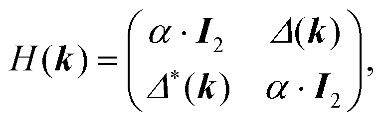
| βSOC = −iνijλSz, |
Fig. 4a and b compare the hcb band structures with and without SOC. Being a light-weight element, the SOC of carbon is tiny (λ = −5.8 × 10⁻⁶β126), and thus creates a tiny band gap of 0.02 meV (see inset of Fig. 4b). Increasing SOC to an unrealistically exaggerated value of 0.1β1 clearly shows the band gap opening and is useful for obtaining the topological properties of 2D polymers (see Fig. 4c).
It is important to note that, while a SOC-induced band gap opening is the necessary condition for a topological state, it is not a sufficient one (i.e., the opened band gap could be between topologically trivial states). The simplest, although neither elegant nor computationally economic, method to see if a topological state is located at the EF is to calculate a nanoribbon, which explicitly yields topological edge states. The left of Fig. 4c shows the band structure of a zigzag hcb nanoribbon with a width of 12 units. The calculation with consideration of SOC yields, besides a more complex band structure due to the reduction of symmetry, both the opened band gap and the states crossing the EF at the place, where the Dirac point has been located.
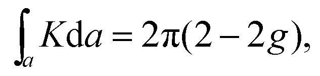
It is worth noting that the topological character of a material is the result of its bulk (interior of the material) and that the topological edge states only manifest at its boundaries. Therefore, topological states can be demonstrated without making the explicit nanoribbon calculations. These calculations require exploitation of space topology and the concept of the Berry phase.27 In mathematics, topology is a geometrical property that will be preserved under deformation. For example, in three dimensions, a sphere with closed surface is characterized by a genus (g) of zero. The genus will be preserved under deformation: any geometrical transformation that maintains the closed surface, e.g., from sphere to any polyhedron, maintains g = 0. A torus (donut-shaped), which possesses a hole, is characterized by g = 1. Topologically, a donut can be converted into any other object with a hole, e.g., into a mug. However, a torus and a sphere cannot be interconverted into each other.
In two dimensions, the topology of an area can be calculated using the Gauss–Bonnet theorem:
Similar to the integration of the Gaussian curvature in the Gauss–Bonnet theorem, when the Berry curvature is integrated within the BZ, it becomes the Berry phase and, with further division by 2π, we get the Chern number, defined as:
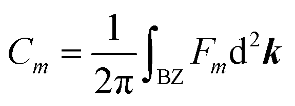
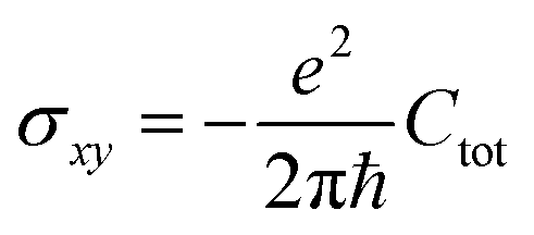
is proportional to the sum of the Chern numbers of all occupied bands, Ctot. The calculated Chern numbers for the hcb structure are 1 and −1 for the lowest and the highest band, respectively, which reconfirms that these bands are truly topologically non-trivial.
The Quantum Spin Hall effect (QSH), discovered by Zhang et al.,28 illustrates best the topologically protected edge states in a topological insulator. However, the spin-dependent topological properties can no longer be characterized by Chern invariants, since the total Chern number will cancel out by the spin-up and spin-down electrons under time reversal symmetry. This new invariant is called Z2 and can be calculated as follows:
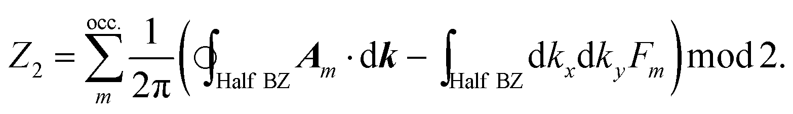
There are various methods proposed to calculate the Z2 invariant, for example, by parity of the wavefunction29 and by the Fukui–Hatsugai method.30 Here, we employ the approach given by Soluyanov and Vanderbilt,31,32 which applies Wannier charge centres (WCCs). By definition, the Wannier functions for band m at a position R can be written as

With these WCCs, one can get the Z2 invariant by drawing lines across half the BZ. For a topologically non-trivial system, any line cutting through the half BZ should cross the WCCs odd times (more details of the procedures are found in the description of the Z2PACK package33). In Fig. 4c, any arbitrary line crossing in the half BZ intersects with the WCCs one time, which demonstrates that the hcb structure is a topologically non-trivial material with Z2 = 1.
3.3 Network-determined electronic band structures and topological properties
Now, we discuss the impact of the network on the electronic properties of a material obeying the network symmetry. We note that in a 2D polymer, the vertices are represented by molecular building blocks (and that a molecule may provide more than one vertex). The distance between two vertices and the degree of π delocalization defines the 1st-neighbour TB hopping elements β1, and longer-ranged delocalization results in non-zero 2nd-neighbour TB hopping elements β2. The number of electrons in the system is given by the molecules representing the vertices and can be controlled by functionalization (e.g., replacing a C atom by a B (N) atom lowers (increases) the number of electrons per unit).12Since the regular nets hxl and sql are formed by only one vertex (see Fig. 1b and c), their band structure contains only one band. It emerges with the vertex of a parabola at the Γ point. If it is half filled, then the system must be metallic. 2nd-neighbour interactions slightly change the band dispersion, and lack of interaction between the vertices (β1 → 0) creates a grid of spin centres. If the band is empty and marks the conduction band (CB), its dispersion determines the effective mass of the charge carriers at the Γ point. If the band is the completely filled valence band (VB), holes would emerge at the M point.
If a second vertex is present in the unit cell, there are also two bands present. This is the case in the hcb lattice, which emerges from the hxl lattice, when every 3rd vertex is removed to form a honeycomb structure. Thus, at the K point, a parabola is missing and all bands cross at the conical intersection, known as the Dirac point. This point also separates all bands in half at the energy scale, which pins the EF to the Dirac point. The 2nd-neighbour interactions modify the band dispersion, but do not affect the highly symmetric conical band structure at the Dirac point, which renders the simple TB approach sufficient for the description of physical phenomena in graphene.
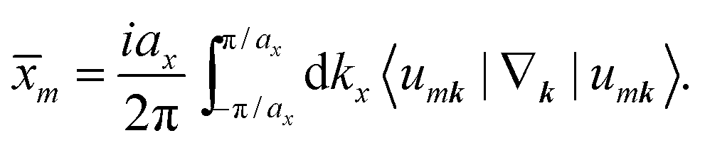
A third vertex per unit cell consequently generates a 3rd band. One of these structures is the kgm lattice, which can be obtained again from the hxl lattice with every 4th vertex removed. Its band structure (see Fig. 5) includes a Dirac point, as known from the hcb lattice, and a flat band that touches the Dirac bands at the Γ point at highest energy. The 2nd-neighbour interaction has only small influence on the band structure. If the band structure is half filled (three electrons in the unit cell), the kgm lattice is metallic. However, if only two electrons per unit cell are present, it has the same features as hcb, and with more than three electrons the flat band is accessed. It is interesting to note at this point that the dispersion of the flat band can be controlled by functionalisation.12
 | ||
| Fig. 5 Band structure of kgm lattice considering only 1st-neighbour (left top), 2nd-neighbour (right top), SOC (left bottom), and 2nd-neighbour with SOC (right bottom) interactions. The Chern numbers C are shown for the individual bands. | ||
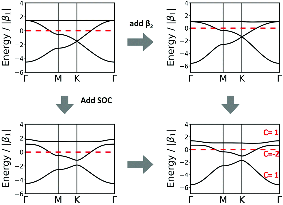
Another interesting structure with three bands is the Lieb lattice, the sql lattice with every 4th vertex removed, resulting in three sites (only one of them strictly is a vertex with 4 links as in the sql lattice, as the other two have only 2 links) per unit cell (Fig. 1 and 6). The resulting band structure, presented in Fig. 6, shows a Dirac point, which is crossed by a flat band. With three electrons per unit cell, EF is located at the Dirac point. The 2nd-neighbour interactions open a small band gap between the flat and the unoccupied bands.
 | ||
| Fig. 6 Band structure of the Lieb lattice. Conventions are as in Fig. 5. Note that inclusion of 2nd-neighbour interactions via the distance criterion yields different values for β2, which would disperse the flat band. | ||
The introduction of SOC mainly affects the high-symmetry points. For sql and hxl, within the TB model, the SOC effects cancel out exactly. For the hcb lattice, which has been discussed in Section 3.2, SOC manifests its topological properties, which are expressed both in the Chern number and in the Z2 invariant. They are easily visible in the crossing bands at the Fermi level, which mark topologically protected linear bands that offer dissipation-free spin transport.
For the kgm lattice, SOC both opens a band gap at the Dirac point and a gap at the touching point between the flat and the Dirac bands at the Γ point. All three bands are topologically non-trivial, as reflected both by the Chern number and the Z2 invariant (see Fig. 5).
In the Lieb lattice, SOC opens a band gap at the Dirac point, but does not shift the flat band. Thus, it creates an interesting electronic structure with heavy electrons in the flat band and massless charge carriers at the frontier bands of the Dirac cone. While the bands forming the Dirac cone are topologically non-trivial, the flat band in the Lieb lattice only exhibits trivial topological properties (see Fig. 6).
3.4 Electronic structure of 2D networks
Tables S1–S4 in the ESI† show the sketches and the corresponding TB electronic structures, including 1st- and 2nd-neighbour interactions as well as spin–orbit coupling, of the following 101 nets: Table S1 (ESI†) shows these for the Platonic nets hcb, hxl, and sql. Table S2 (ESI†) contains these diagrams for the Archimedean nets cem, fes, fsz, fxt, hca, htb, kgm, and tts. The demiregular nets bew, cph, kra, krb, krc, krd, kre, krf, krg, krh, krj, krk, krl, krm, krn, krq, krr, krs, krt, and usm are listed in Table S3 (ESI†). Table S4 (ESI†) contains the bex, bey, bhd, car, cem-d, cpa, cpb, cpc, cpd, cpe, cpf, cpg, cpj, cpk, cpl, cpm, cpn, cpo, cpp, cpq, cpr, cps, cpt, cpu, cpv, cpw, cpx, cpy, cpz, cqa, cqb, cqc, cqd, cqg, cqp, cqr, cru, crz, dha, dhb, esq, fwb, fwe, hca-a, hna, hnb, htb-a, jvh, kgd, kgd-a, kru, krv, krw, krx, kry, mcm, mtf, pnb, pnd, pne, pnf, png, pnh, sdb, sdc, sdd, sde, sdf, stz, and suz nets.4 Fostering topological properties
As we have shown in Section 3, important features of a 2D material's band structure emerge from the network topology. In particular, topological properties are directly related to the connectivities of the network. We have identified a large number of networks with intriguing electronic, potentially topological, properties. As 2D polymers are made of light elements only, the magnitude of SOC is small, and the emerging band gaps are in the range of only ∼20 μeV. Hence, these properties can only be probed at extremely cryogenic conditions and, therefore, their applications are restricted. Recently, Burkard's group has shown that the SO-induced band gap in graphene can be significantly increased if the material is interfaced with a transition metal dichalcogenide under a magic angle.34 Such effect is likely possible also for 2D polymers.A chemical way to increase the band gap is a smart application of quantum confinement: graphene nanoribbons open a band gap because of their finite width, and if the ribbons are appropriately shaped, they maintain their topological properties, thus yielding topological insulators with large band gap.35–37
Here, we will explore a different, chemical, route to create 2D topological insulators: We aim to open the band gap at topologically non-trivial points by the reduction of symmetry in the 2D nets. This approach will be illustrated in the remainder of this section.
For the Platonic lattices sql, hxl, and hcb, and also for the Archimedean net kgm, all vertices and edges are chemically equal, and lattice symmetry reduction is no simple means for controlling the electronic and topological properties.
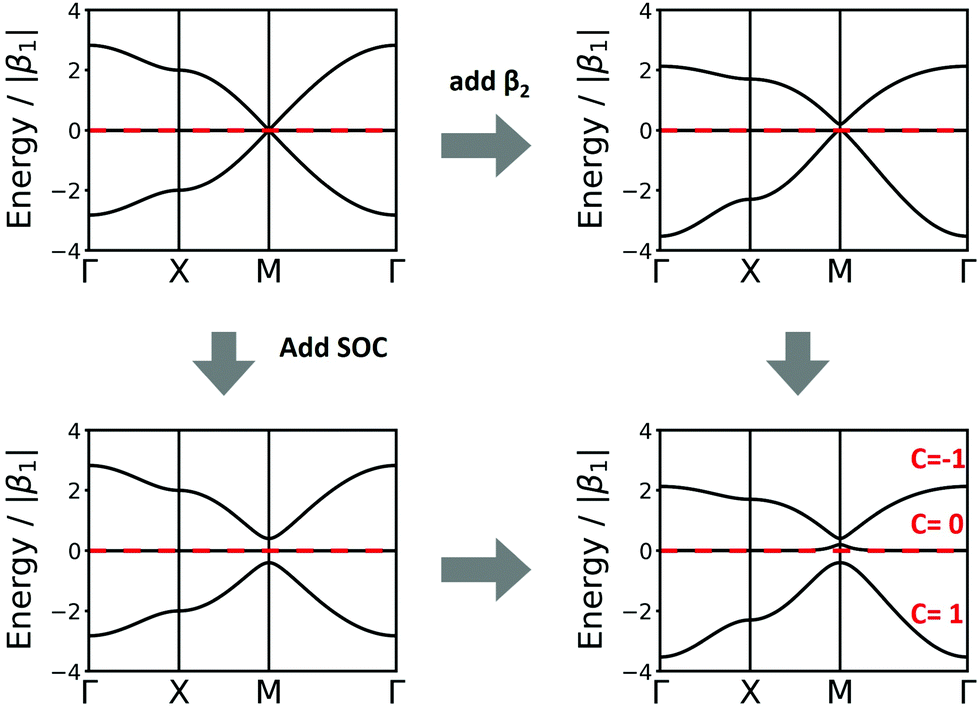
The Lieb lattice has two different sites: one type is the vertex connected to four neighbours, while the second type is a site located at the edges connected to two neighbours. The links are all identical. As the two symmetrically distinct sites are to be represented by two different molecular building blocks (see Section 5), they likely have a different chemical potential that is expressed in two different values of α in the TB approach. Indeed, this change of α opens a band gap at the Dirac point. For simplicity, we demonstrate the effect with bands only considering 1st-neighbour interactions. Interestingly, if the chemical potential of the four-connected-vertex is lower than that of the linear site (see Fig. 7), the gap opening is below the flat band, while it is above if the chemical potential of the linear site is lower. Note, that in both cases one of the Dirac bands touches the flat band. The band opening due to different chemical potentials enhances the SOC-induced band opening discussed in Section 3.3, while the topological signatures of the three bands remain unchanged. Thus, reduction of symmetry can enhance gaps at topological points, and offers a promising way towards the realization of room-temperature 2D topological materials.
 | ||
| Fig. 7 Lieb band structures considering only 1st-neighbour interactions and different onsite energies, α. | ||
The fes lattice (Fig. 8) has identical vertices, but different symmetry in the edges, which are either between octagons (red in Fig. 8) or between a square and an octagon (black in Fig. 8). In the TB model with identical hopping elements β1, it shows two high-symmetry crossing points (Γ and M), both with three bands, one being locally flat, while the other two cross at a Dirac point. These degeneracies are broken under the effect of SOC, and all four bands are topologically non-trivial (see Fig. 8a). As different molecular linkers will represent the different edges in a 2D polymer, the system must be described with different values of β1. As shown in Fig. 8, this symmetry reduction opens band gaps at the same high-symmetry points, similarly as in the Lieb lattice. Depending on the value for the SOC, the resulting bands can change their Chern numbers.
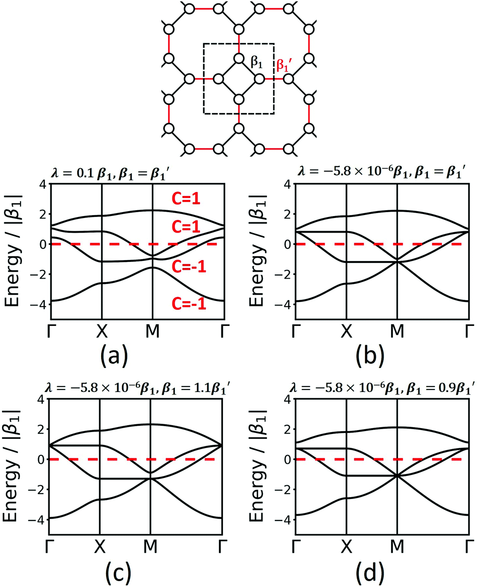 | ||
| Fig. 8 Band structures of fes: (a) considering 1st and 2nd neighbours and SOC, (b–d) considering only 1st-neighbour interaction with identical and different values of the hopping matrix elements β1 and β1′. | ||
Finally, we study the krb lattice (see Fig. 9) as a member of the demiregular nets. The unit cell contains eight sites, two with six neighbours (black labels) and six with four neighbours (white labels), which produce eight bands. The two different edges are coloured black and blue. The band structure shows some nearly degenerate lattice points at M, K, and Γ. All the four lower bands are topologically trivial. Yet, having two different vertices and two different edges allows a wide range of electronic structure modification, as both α and β1 can have different values. Similar as in the Lieb lattice, modifying the onsite elements opens band gaps at the Γ point. Hopping elements affect the general dispersion of the bands. We conclude that there are rational design rules for applying chemically sensible concepts of chemical potential shifts and adjusting π-conjugation that can be applied to design both topological and classical 2D polymers with application-tailored electronic properties.
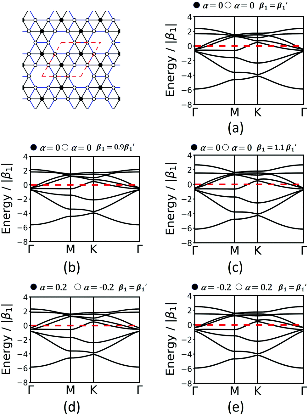 | ||
| Fig. 9 Band structures of krb considering only 1st-neighbour interactions (a), modification of the hopping elements (b and c) and onsite elements (d and e). Conventions are as in Fig. 7 and 8. | ||
5 Realizing 2D nets in 2D polymer structures
In order to form 2D polymers with the correct topology, molecular building blocks have to be assembled. The required shape and symmetry of vertices and edges can be obtained by analysing the topology diagram of the required net as demonstrated in several reviews.2,38–41 Such a topology diagram can be found in Fig. 10. While edges are in general linear and do not impose any additional requirements, vertices need to have the correct rotational symmetry. The 200 different 2D nets in the RCSR database include vertices with coordination numbers from 3 to 12.20 The most abundant ones are vertices with 3, 4, and 6 neighbours. Thus, monomers need to have a C3, C4 (or, with four connecting points but broken symmetry, C2), and C6 rotational axis to serve as such vertices, respectively. In addition, C2 monomers can be placed on edges. In order to give examples for these cases, Fig. 10 shows how hxl, hcb, sql, and kgm nets can be deconstructed into vertices and edges along with examples of monomers.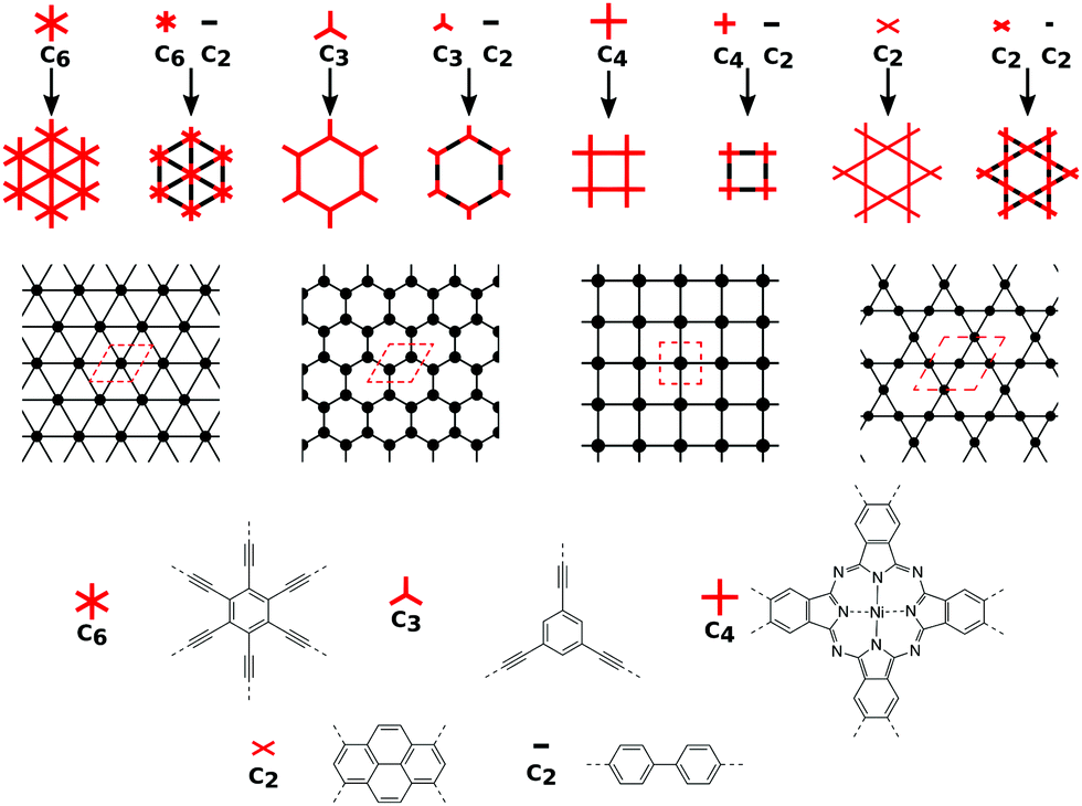 | ||
| Fig. 10 Topology diagrams for hxl, hcb, sql, and kgm nets with and without pronounced linkers along with corresponding 2D representations (with the unit cells marked in red) are shown at the top of the figure. The bottom of the figure shows suggestions for simple nodes with 2-, 3-, 4-, and 6-fold rotational symmetry and a linear linker. | ||
These nets can be obtained both by self-condensation of a vertex with the respective rotational symmetry or by the connection of such a monomer with a linker. Already in the 1980s, γ-graphyne was proposed as an example of the hxl net.42 In this material, benzene vertices are connected by ethynyl groups. For conjugated polymers with the hcb topology, the triangular vertices (C3 rotational symmetry) are often benzene rings, condensed benzene rings, or, so far only considered in computational studies, also simple tertiary butyl radicals.9,13,43–45 For the sql net, the usual C4 building blocks of choice are either porphyrins or phthalocyanines, which offer lattice angles of 90°.14,46 However, using pyrene or tetraethylethene as building blocks with four connectors (with rotational symmetry reduced to C2) can lead to a plethora of distorted sql structures.10,13,14,47 Here, although the angle between the cell vectors differ from 90°, the 2D polymer is still in the sql topology, because of the connectivity and identity of vertices. Similarly, tetraethylethene vertices can also be used to realize the kgm net in 2D polymers.47 Employment of conjugated five-membered rings can lead to the formation of a 2D polymer with the unusual htb topology.48 In addition to the very popular nets, also rather complex nets, such as the bex net, have recently been synthesized.49 A 2D polymer with an electronic structure corresponding to the Lieb lattice exhibiting Stoner ferromagnetism was reported by Jiang et al. (see Fig. 11).15
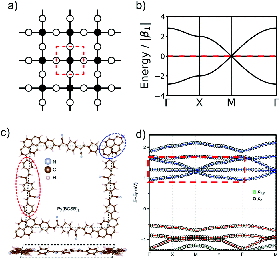 | ||
Fig. 11 The schematic representation of Lieb lattice (a) and the corresponding TB band structure (b). (c) Top and side views of crystal structure of Py(BCSB)2 with Py (blue ellipse) and BCSB (red ellipse) ligands sitting on the corner and edge-center sites of the distorted Lieb lattice, respectively. (d) DFT calculated electronic band structure for kz![[thin space (1/6-em)]](https://www.rsc.org/images/entities/char_2009.gif) = 0 plane and the orbital-resolved projected band for pz (black circle) and px,y (green circle) orbitals. The red and blue bands highlight the Lieb-3 and Lieb-5 band structure, respectively. Lieb signature comparable with (b) is marked by red dashed rectangle in the conduction band. (c and d) Adapted with permission from ref. 13, Copyright 2019, Springer Nature. = 0 plane and the orbital-resolved projected band for pz (black circle) and px,y (green circle) orbitals. The red and blue bands highlight the Lieb-3 and Lieb-5 band structure, respectively. Lieb signature comparable with (b) is marked by red dashed rectangle in the conduction band. (c and d) Adapted with permission from ref. 13, Copyright 2019, Springer Nature. | ||
As linkers, both ethynyl building blocks (so far mostly in computational studies) and benzene rings, being connected to the vertices by imine linkages, have been used.9,10,13,14,45,47 They are both simple, guarantee conjugation, and are rather rigid. However, orbital overlap can be reduced, if benzene units have a dihedral angle with respect to the planar vertices. Therefore, it is important to design linkers in a way that they remain as planar as possible. In linkers consisting of condensed benzene rings, however, the connectivity forces the system to be planar. In this case, π-orbital overlap is maximized.44,46 Formation of disperse bands can be improved, if the energies of frontier orbitals in the molecular building blocks, representing vertices and edges, match.15 The strength of the electronic coupling between the monomers can be estimated by looking at the electron delocalization in dimer models.14 A good example for controlling the band structure in 2D polymers is the combined kgm–hcb net as shown in Fig. 12.12 The lattice is built of heterotriangulenes, in which the centre atom can be B, C or N, thus creating an unoccupied, half-occupied or fully occupied centre site. Accordingly, EF is located below the Dirac bands (B), at the Dirac point (C) or above the Dirac bands (N) (Fig. 12a–c). The dispersion of the bands, most visible in the flat bands, is strongly affected by the bridge groups in the monomer compounds, which can be chosen as CO, CH2 or O. In the case of the monomers with B centre atoms, a flat band marks the valence band maximum. The effective masses of the holes can range from 1.6 me to infinity (see Fig. 12d–f).
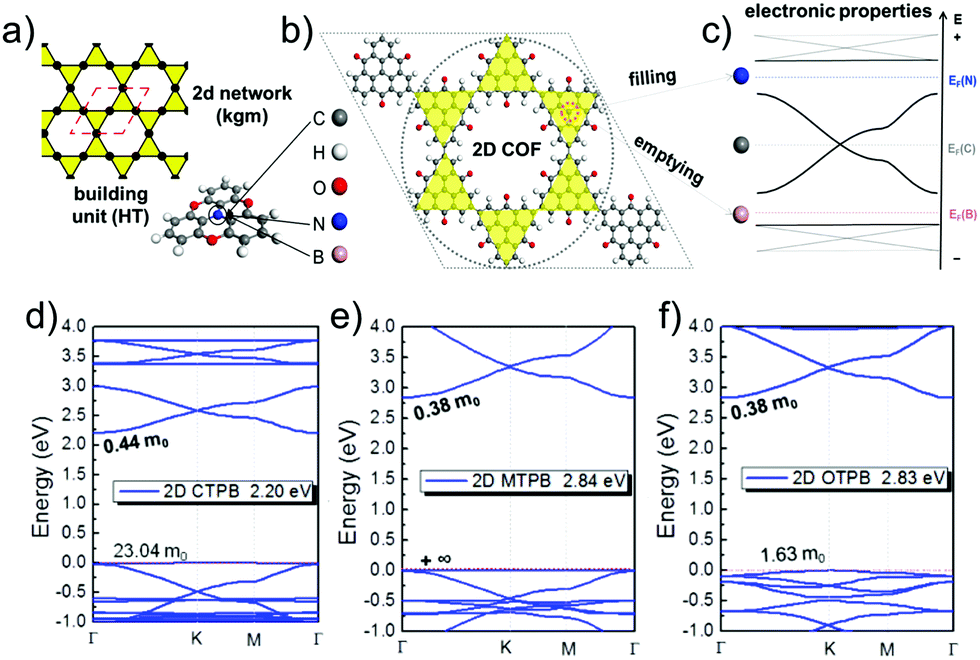 | ||
| Fig. 12 The schematic of kgm lattice (a) together with atomistic structure of a 2D polymer based on heterotriangulenes (b) and the corresponding band structure (c) revealing signatures of kgm (cf.Fig. 5). Depending on number of electrons, EF is shifted below the Dirac band (B), to the Dirac point (C), or to the top of the Dirac band (N). Functionalization by B and N gives access to the flat bands emerging from the kgm lattice. Heterotriangulenes with three different bridge groups, namely (d) keto, (e) CH2, and (f) ether, show different impact on the dispersion of the flat bands. The band structure is a superposition of the kgm and hcb network, both are found in the structure of this 2D polymer. Adapted with permission from ref. 10, Copyright 2019, American Chemical Society. | ||
Topological phases can only be obtained, if topological bands are in the vicinity of EF. In addition to the previous prerequisites, for some systems, it might be necessary to shift EF to a position that is topologically non-trivial. This could be achieved by functionalization12 (Fig. 12a and c) and, to some extent, by doping.
Suitable coupling reactions, which retain the π-conjugation, are discussed by others in detail in this Special Issue or in the paper of Liu et al.50
6 Outlook and perspectives
The discovery of topological insulators has marked a breakthrough in condensed matter physics, but the realization of this state of matter in room temperature applications remains unsolved. It is well known that lattices can impose topological features, as it has been demonstrated for photonic crystals, for example in the optical Lieb lattice.51–54 While this approach allows studying the lattice-imposed topological effects, the restriction to bosonic particles limits applications. It is, therefore, intriguing to realize topological networks in materials.Recently, the Lieb lattice has been experimentally realized by forming its edges and vertices by the surface state electrons of Cu(111) confined by an array of carbon monoxide molecules23 or by vacancy defects of chlorine superstructure on Cu(100) surface.22 These structures are, however, only stable at cryogenic temperatures (<5 K).
On the other hand, the relatively recent field of framework materials, including metal–organic frameworks and covalent-organic frameworks, and of 2D polymers, offers the realization of virtually any network structure that is stable at room temperature. This offers an additional means to introduce functionality to chemistry, namely by the structural topology of the network. In this review, we scratched the surface of the possibilities by concentrating on materials realizing topological 2D networks.
The collection of over 200 networks, included in the Reticular Chemistry Structural Resource database,20 offers a huge variety of possible skeletons for actual 2D materials, which can be created by a proper selection of molecular building blocks. The topological properties of the hypothetical 2D nets could then be realized in the corresponding 2D arrangement of such building blocks. As we have shown in this tutorial, the creation of 2D polymers with building blocks that offer long-range π-conjugation is a very promising route to realize topological networks with high crystallinity and extended π-conjugation. Here, we have demonstrated how the topological properties of the nets can be predicted, how atomistic structures of materials can be generated, and we have shown examples for their successful realization in experiments. The crucial step of synthesizing these materials is covered in an article by other authors in this Special Issue.
One of the grand challenges that remains to be solved is to design building blocks that include an active site, which typically means an unsaturated π electron. That is, the building blocks must either be π radicals, which still can undergo the pre-designed linkage reactions. Alternatively, after polymerization the number of π electrons can be controlled, e.g., by post-synthetic functionalization or by gating.
The second grand challenge is to control the level of defects, including structural and substitutional ones. The third, related grand challenge is the formation of highly crystalline networks, as high crystallinity is the precondition for the robustness of the topological properties. This includes the rigidity of the frameworks, as strong lattice vibrations may be sufficient to make the topological properties collapse.
Given the immense progress in the chemistry of 2D polymers and the recent enhancement of interdisciplinary collaborations between condensed matter physicists and chemists, e.g., manifested in research on graphene nanoribbons,35,36 we are confident that these challenges can be met during the next decade.
What we have not touched in this review is the additional functionality that arises from interlayer interactions: in multi-layers and heterostructures, it is expected that the properties of these 2D materials are further modified, as known for other 2D materials, including graphene or transition metal dichalcogenides. We have covered this subject in a recent perspective article, to which we refer the interested reader.55
Conflicts of interest
There are no conflicts to declare.Acknowledgements
Financial support by Deutsche Forschungsgemeinschaft (HE 3543/27-1, HE 3543/31-1) and high-performance computer time granted by ZIH Dresden is gratefully acknowledged.Notes and references
- D. Akinwande, C. J. Brennan, J. S. Bunch, P. Egberts, J. R. Felts, H. Gao, R. Huang, J.-S. Kim, T. Li, Y. Li, K. M. Liechti, N. Lu, H. S. Park, E. J. Reed, P. Wang, B. I. Yakobson, T. Zhang, Y.-W. Zhang, Y. Zhou and Y. Zhu, Extreme Mech. Lett., 2017, 13, 42–77 CrossRef.
- X. Feng, X. Ding and D. Jiang, Chem. Soc. Rev., 2012, 41, 6010–6022 RSC.
- A. P. Côté, A. I. Benin, N. W. Ockwig, M. O’Keeffe, A. J. Matzger and O. M. Yaghi, Science, 2005, 310, 1166–1170 CrossRef PubMed.
- S.-Y. Ding and W. Wang, Chem. Soc. Rev., 2013, 42, 548–568 RSC.
- M. Bieri, S. Blankenburg, M. Kivala, C. A. Pignedoli, P. Ruffieux, K. Müllen and R. Fasel, Chem. Commun., 2011, 47, 10239 RSC.
- C. Steiner, J. Gebhardt, M. Ammon, Z. Yang, A. Heidenreich, N. Hammer, A. Görling, M. Kivala and S. Maier, Nat. Commun., 2017, 8, 14765 CrossRef CAS PubMed.
- F. Schlütter, F. Rossel, M. Kivala, V. Enkelmann, J.-P. Gisselbrecht, P. Ruffieux, R. Fasel and K. Müllen, J. Am. Chem. Soc., 2013, 135, 4550–4557 CrossRef PubMed.
- W. Wang and A. D. Schlüter, Macromol. Rapid Commun., 2019, 40, e1800719 CrossRef PubMed.
- X. Zhuang, W. Zhao, F. Zhang, Y. Cao, F. Liu, S. Bi and X. Feng, Polym. Chem., 2016, 7, 4176–4181 RSC.
- E. Jin, M. Asada, Q. Xu, S. Dalapati, M. A. Addicoat, M. A. Brady, H. Xu, T. Nakamura, T. Heine, Q. Chen and D. Jiang, Science, 2017, 357, 673–676 CrossRef CAS PubMed.
- R. Dong, P. Han, H. Arora, M. Ballabio, M. Karakus, Z. Zhang, C. Shekhar, P. Adler, P. S. Petkov, A. Erbe, S. C. B. Mannsfeld, C. Felser, T. Heine, M. Bonn, X. Feng and E. Cánovas, Nat. Mater., 2018, 17, 1027–1032 CrossRef CAS PubMed.
- Y. Jing and T. Heine, J. Am. Chem. Soc., 2019, 141, 743–747 CrossRef CAS PubMed.
- S. Thomas, H. Li, C. Zhong, M. Matsumoto, W. R. Dichtel and J.-L. Bredas, Chem. Mater., 2019, 31, 3051–3065 CrossRef CAS.
- S. Thomas, H. Li, R. R. Dasari, A. M. Evans, I. Castano, T. G. Allen, O. G. Reid, G. Rumbles, W. R. Dichtel, N. C. Gianneschi, S. R. Marder, V. Coropceanu and J.-L. Brédas, Mater. Horiz., 2019, 6, 1868–1876 RSC.
- W. Jiang, H. Huang and F. Liu, Nat. Commun., 2019, 10, 2207 CrossRef PubMed.
- F. Crasto de Lima, G. J. Ferreira and R. H. Miwa, Phys. Chem. Chem. Phys., 2019, 21, 22344–22350 RSC.
- H. Sahabudeen, H. Qi, B. A. Glatz, D. Tranca, R. Dong, Y. Hou, T. Zhang, C. Kuttner, T. Lehnert, G. Seifert, U. Kaiser, A. Fery, Z. Zheng and X. Feng, Nat. Commun., 2016, 7, 13461 CrossRef CAS PubMed.
- L. Ascherl, T. Sick, J. T. Margraf, S. H. Lapidus, M. Calik, C. Hettstedt, K. Karaghiosoff, M. Doblinger, T. Clark, K. W. Chapman, F. Auras and T. Bein, Nat. Chem., 2016, 8, 310–316 CrossRef CAS.
- D. Chavey, Symmetry 2, Elsevier, 1989, pp. 147–165 Search PubMed.
- M. O’Keeffe, M. A. Peskov, S. J. Ramsden and O. M. Yaghi, Acc. Chem. Res., 2008, 41, 1782–1789 CrossRef PubMed.
- N. L. Smirnova, Crystallogr. Rep., 2009, 54, 743–748 CrossRef CAS.
- R. Drost, T. Ojanen, A. Harju and P. Liljeroth, Nat. Phys., 2017, 13, 668–671 Search PubMed.
- M. R. Slot, T. S. Gardenier, P. H. Jacobse, G. C. P. van Miert, S. N. Kempkes, S. J. M. Zevenhuizen, C. M. Smith, D. Vanmaekelbergh and I. Swart, Nat. Phys., 2017, 13, 672–676 Search PubMed.
- M. Scholz, Z. Chem., 2010, 11, 239 Search PubMed.
- P. Hofmann, Solid state physics: an introduction, Wiley-VCH, Verlag GmbH & Co. KGaA, Weinheim, 2nd edn, 2015 Search PubMed.
- C. L. Kane and E. J. Mele, Phys. Rev. Lett., 2005, 95, 226801 CrossRef CAS PubMed.
- M. Z. Hasan and C. L. Kane, Rev. Mod. Phys., 2010, 82, 3045–3067 CrossRef CAS.
- M. Konig, S. Wiedmann, C. Brune, A. Roth, H. Buhmann, L. W. Molenkamp, X.-L. Qi and S.-C. Zhang, Science, 2007, 318, 766–770 CrossRef PubMed.
- L. Fu and C. L. Kane, Phys. Rev. B: Condens. Matter Mater. Phys., 2007, 76, 045302 CrossRef.
- T. Fukui and Y. Hatsugai, J. Phys. Soc. Jpn., 2007, 76, 053702 CrossRef.
- A. A. Soluyanov and D. Vanderbilt, Phys. Rev. B: Condens. Matter Mater. Phys., 2011, 83, 035108 CrossRef.
- A. A. Soluyanov and D. Vanderbilt, Phys. Rev. B: Condens. Matter Mater. Phys., 2011, 83, 235401 CrossRef.
- D. Gresch, G. Autès, O. V. Yazyev, M. Troyer, D. Vanderbilt, B. A. Bernevig and A. A. Soluyanov, Phys. Rev. B, 2017, 95, 075146 CrossRef.
- A. David, P. Rakyta, A. Kormányos and G. Burkard, Phys. Rev. B, 2019, 100, 085412 CrossRef CAS.
- D. J. Rizzo, G. Veber, T. Cao, C. Bronner, T. Chen, F. Zhao, H. Rodriguez, S. G. Louie, M. F. Crommie and F. R. Fischer, Nature, 2018, 560, 204–208 CrossRef CAS PubMed.
- O. Gröning, S. Wang, X. Yao, C. A. Pignedoli, G. Borin Barin, C. Daniels, A. Cupo, V. Meunier, X. Feng, A. Narita, K. Müllen, P. Ruffieux and R. Fasel, Nature, 2018, 560, 209–213 CrossRef PubMed.
- T. Cao, F. Zhao and S. G. Louie, Phys. Rev. Lett., 2017, 119, 076401 CrossRef PubMed.
- Y. H. Xu, S. B. Jin, H. Xu, A. Nagai and D. L. Jiang, Chem. Soc. Rev., 2013, 42, 8012–8031 RSC.
- N. Huang, P. Wang and D. Jiang, Nat. Rev. Mater., 2016, 1, 6010 Search PubMed.
- N. Huang, L. Zhai, D. E. Coupry, M. A. Addicoat, K. Okushita, K. Nishimura, T. Heine and D. Jiang, Nat. Commun., 2016, 7, 12325 CrossRef PubMed.
- D. Jiang, X. Chen, K. Geng, R. Liu, K. T. Tan, Y. Gong, Z. Li, S. Tao and Q. Jiang, Angew. Chem., Int. Ed., 2019, 58, 2–44 CrossRef.
- R. H. Baughman, H. Eckhardt and M. Kertesz, J. Chem. Phys., 1987, 87, 6687–6699 CrossRef CAS.
- J.-J. Adjizian, P. Briddon, B. Humbert, J.-L. Duvail, P. Wagner, C. Adda and C. Ewels, Nat. Commun., 2013, 4, 2736 CrossRef PubMed.
- J. Guo, Y. Xu, S. Jin, L. Chen, T. Kaji, Y. Honsho, M. A. Addicoat, J. Kim, A. Saeki, H. Ihee, S. Seki, S. Irle, M. Hiramoto, J. Gao and D. Jiang, Nat. Commun., 2013, 4, 2736 CrossRef PubMed.
- L. Bai, Q. Gao and Y. Zhao, J. Mater. Chem. A, 2016, 4, 14106–14110 RSC.
- M. Wang, M. Ballabio, M. Wang, H.-H. Lin, B. P. Biswal, X. Han, S. Paasch, E. Brunner, P. Liu, M. Chen, M. Bonn, T. Heine, S. Zhou, E. Cánovas, R. Dong and X. Feng, J. Am. Chem. Soc., 2019, 141, 16810–16816 CrossRef CAS PubMed.
- Z.-F. Pang, T.-Y. Zhou, R.-R. Liang, Q.-Y. Qi and X. Zhao, Chem. Sci., 2017, 8, 3866–3870 RSC.
- S.-L. Cai, Z.-H. He, X.-L. Li, K. Zhang, S.-R. Zheng, J. Fan, Y. Liu and W.-G. Zhang, Chem. Commun., 2019, 55, 13454–13457 RSC.
- T. Banerjee, F. Haase, S. Trenker, B. P. Biswal, G. Savasci, V. Duppel, I. Moudrakovski, C. Ochsenfeld and B. V. Lotsch, Nat. Commun., 2019, 10, 2689 CrossRef PubMed.
- X.-H. Liu, C.-Z. Guan, D. Wang and L.-J. Wan, Adv. Mater., 2014, 26, 6912–6920 CrossRef CAS PubMed.
- R. Shen, L. B. Shao, B. Wang and D. Y. Xing, Phys. Rev. B: Condens. Matter Mater. Phys., 2010, 81, 041410 CrossRef.
- S. Mukherjee, A. Spracklen, D. Choudhury, N. Goldman, P. Öhberg, E. Andersson and R. R. Thomson, Phys. Rev. Lett., 2015, 114, 245504 CrossRef PubMed.
- S. Taie, H. Ozawa, T. Ichinose, T. Nishio, S. Nakajima and Y. Takahashi, Sci. Adv., 2015, 1, e1500854 CrossRef PubMed.
- R. A. Vicencio, C. Cantillano, L. Morales-Inostroza, B. Real, C. Mejía-Cortés, S. Weimann, A. Szameit and M. I. Molina, Phys. Rev. Lett., 2015, 114, 245503 CrossRef PubMed.
- A. Kuc, M. Springer, K. Batra, R. Juarez-Mosqueda, C. Wöll and T. Heine, Adv. Funct. Mater., 2020, 1908004 CrossRef.
Footnotes |
| † Electronic supplementary information (ESI) available: Contains sketches of total of 101 topologies with their tight-binding band structures, accounting for the 1st-neighbour, 2nd-neighbour, and spin–orbit interactions. See DOI: 10.1039/c9cs00893d |
| ‡ Equal contribution. |
| This journal is © The Royal Society of Chemistry 2020 |