
 Open Access Article
 This Open Access Article is licensed under a
 Creative Commons Attribution 3.0 Unported Licence
Organic field-effect transistor-based flexible sensors†
Saravanan
Yuvaraja‡
 a,
Ali
Nawaz‡
bc,
Qian
Liu
d,
Deepak
Dubal
de,
Sandeep G.
Surya
*a,
Khaled N.
Salama
*a and
Prashant
Sonar
*de
a,
Ali
Nawaz‡
bc,
Qian
Liu
d,
Deepak
Dubal
de,
Sandeep G.
Surya
*a,
Khaled N.
Salama
*a and
Prashant
Sonar
*de
aSensors Lab, Advanced Membranes and Porous Materials Center, Computer, Electrical and Mathematical Science and Engineering Division, King Abdullah University of Science and Technology, Saudi Arabia. E-mail: sandeep.surya@kaust.edu.sa; khaled.salama@kaust.edu.sa
bDepartamento de Física, Universidade Federal do Paraná, Caixa Postal 19044, 81531-990, Curitiba, PR, Brazil
cBrazilian Nanotechnology National Laboratory (LNNano), Brazilian Center for Research in Energy and Materials (CNPEM), 13083-970, Campinas, São Paulo, Brazil
dSchool of Chemistry and Physics, Queensland University of Technology (QUT), Brisbane, QLD 4000, Australia. E-mail: sonar.prashant@qut.edu.au
eCentre for Materials Science, Queensland University of Technology, 2 George Street, Brisbane, QLD 4000, Australia
First published on 19th May 2020
Abstract
Flexible electronic devices have attracted a great deal of attention in recent years due to their flexibility, reduced complexity and lightweight. Such devices can conformably attach themselves to any bendable surface and can possess diverse transduction mechanisms. Consequently, with continued emphasis on innovation and development, major technological breakthroughs have been achieved in this area. This review focuses on the advancements of using organic field-effect transistors (OFETs) in flexible electronic applications in the past 10 years. In addition, to the above mentioned features, OFETs have multiple advantages such as low-cost, readout integration, large-area coverage, and power efficiency, which yield synergy. To begin with, we have introduced organic semiconductors (OSCs), followed by their applications in various device configurations and their mechanisms. Later, the use of OFETs in flexible sensor applications is detailed with multiple examples. Special attention is paid to discussing the effects induced on physical parameters of OFETs with respect to variations in external stimuli. The final section provides an outlook on the mechanical aspects of OSCs, activation and revival processes of sensory layers, small area analysis, and pattern recognition techniques for electronic devices.
 Saravanan Yuvaraja | Saravanan Yuvaraja received his bachelor's degree from Anna University, India, in Electronics and Communication Engineering with a first class in 2016. He also competed his MTech degree from Amity University, India, in the field of Solar and Alternative Energy Engineering in 2018. He is currently a PhD candidate in the Sensor Lab Group under the direction of Prof. Khaled Nabil Salama at King Abdullah University of Science in Saudi Arabia. His research interests are in developing flexible and wearable chemical sensors using organic semiconductors and metal organic frameworks on organic field effect transistor (OFET) chemiresistive, chemicapacitive platforms. |
 Ali Nawaz | Dr Ali Nawaz performed his postdoctoral research work at LNNano/CNPEM, Campinas, Brazil, working on the development of nanomembrane-based vertical organic transistors and sensors. He obtained his PhD in Physics from UFPR, Curitiba, Brazil (under the guidance of late Prof. Ivo A. Hümmelgen), where he was involved in the improvement of charge transport properties of low-voltage planar organic transistors. His research expertise and interests include organic transistors, sensors, device physics and engineering, micro-/nano-fabrication of organic devices and process development. |
 Qian Liu | Qian Liu received his MS degree from the Ocean University of China (OUC) in 2014 with joint supervision at Qingdao Institute of Bioenergy and Biotechnology (QIBEBT), Chinese Academy of Sciences (CAS). He is currently a PhD candidate at the School of Chemistry and Physics, Queensland University of Technology (QUT). His research interests focus on the design and synthesis of organic semiconducting materials based on dye molecules and their applications in various types of electronic devices. |
 Sandeep G. Surya | Sandeep G. Surya is a Postdoctoral Research Fellow at King Abdullah University of Science and Technology (KAUST), Kingdom of Saudi Arabia. He received his PhD degree from IIT Bombay and BTech degree from JNTU, Hyderabad. He worked as a Research Associate at Microsystems Technology Research Unit, CMM, Fondazione Bruno Kessler (FBK), Trento, Italy. He was a member of different teams working on explosive detectors and on Telemedicine. His work won the “Young Achiever Award” at IBAE-2019, GYTI AWARD at IIM-A 2012, the Fellowship at ISED 2011, and the P.P CHHABRIA AWARD OF EXCELLENCE in intelligent systems and robotics for the year 2009 at IIIT, Pune. |
 Khaled N. Salama | Khaled Nabil Salama received his BS degree from the Department of Electronics and Communications, Cairo University, Egypt, and his MS and PhD degrees from the Department of Electrical Engineering, Stanford University, USA, in 2000 and 2005. He was an Assistant Professor at Rensselaer Polytechnic Institute, NY, USA, between 2005 and 2009. He joined King Abdullah University of Science and Technology in January 2009, where he is now a professor and was the founding Program Chair until August 2011. He is the director of the Sensors Initiative, a consortium of 9 international universities. His work on CMOS sensors for molecular detection has been funded by NIH and DARPA, awarded the Stanford–Berkeley Innovators Challenge Award in biological sciences and was acquired by Illumina Inc. He is the author of 300 papers and 20 US patents on low-power mixed signal circuits for intelligent fully integrated sensors and neuromorphic circuits using memristor devices. |
 Prashant Sonar | Prashant Sonar performed doctoral work at the Max-Planck Institute of Polymer Research, Mainz, Germany and was awarded PhD in 2004. He then moved to Swiss Federal Institute of Technology (ETH), Zurich, Switzerland, for his postdoctoral research from 2004 till 2006. From 2006 till 2014, he was working as a Research Scientist at the Institute of Materials Research and Engineering (IMRE), Agency of Science, Technology and Research (A*STAR), Singapore. Dr Sonar received the prestigious Future Fellowship (2013) from the Australian Research Council and was appointed an Associate Professor in July 2014 at Queensland University of Technology (QUT), Australia. A/Prof. Sonar is a Fellow of the Royal Society of Chemistry (FRSC) and a Foreign Fellow of the Maharashtra Academy of Sciences (FFMAS) and is currently serving as an Associate Editor of the journal Flexible and Printed Electronics, Material Research Express. He leads the Organic Electronic group at QUT and has published 147 peer-reviewed research papers and filed 11 patents to date. |
1. Introduction
1.1 Importance of flexible and wearable electronics
Wearable electronics have undergone a great evolution in the past few decades. While these devices have existed for several centuries—including inventions like portable and wearable clocks1 and Nuremberg eggs in the 16th century2—only lately have they attracted significant attention in both academic and industrial fields. The progress in this technology can be seen, for example, by the advancement from pocket watches and wristwatches to current smartwatches such as the Apple watch and from phones to smartphones that can perform multiple modern-day functions. In addition, with ever-growing technological advancements in the Internet of Things (IoT), the wearable electronics industry met with increasing demands regarding futuristic applications that can be comfortably worn and readily blended into daily life.3 The wearable device market is estimated to be worth approximately $67 billion by 2024, and it is expected that more than 1 trillion sensors will be designed and implemented in wearable electronics.Wearable electronics is currently becoming increasingly prevalent in many aspects of life, including sports, communications, health and wellness, expenditure tracking and wireless payment, wireless keys, socialization, and so forth.4 Fitness devices, to some extent, have dominated the wearable electronics market because of their universality and low cost. Such products not only help consumers in achieving their fitness goals but also allow them to conveniently perform numerous other functions such as listening to music and conducting video conference calls.
Another important application of wearable electronics lies in the medical area where the flexible sensors can be integrated into clothes or implanted in the human body to monitor the health and performance of a patient.5 Such wearable sensors can further allow the detection of glucose, lactic acid, or uric acid by noninvasive chemical analysis of sweat, tears, or saliva without disrupting the outermost protective layers of the body's skin, which further reduces the risk of harm or infection.
Despite many significant advances, the utilization of rigid substrates (generally glass) in electronic devices still reduces the integration density of wearable applications, especially in skin-like electronics, such as medical treatment and implants, artificial skin and prosthetics, and biological studies. Therefore, developing electronic devices with flexible substrates is an urgent and cutting-edge research topic. Thus, several academic groups have dedicated their efforts to study devices based on mechanical flexibility and stretchability of materials.6,7 The sensor component in electronic devices plays a significant role and can be considered the most fundamental part of wearable electronics. For example, the development of e-skin requires many sensor components to stimulate the response of human skin to external stimuli.8
As the examples above illustrate, flexible and wearable sensors are presently a topic of interest since they can enlarge the application scope and accelerate the advancement of wearable electronics. For instance, development of physical sensors such as strain sensors for electronic skin (e-skin) platforms has recently gained more attention. The most pressing challenges in developing e-skin based sensors stem from the material behavior problems such as poor mechanical stability, diverse sensing behavior and weak self-healing power. Unlike other materials, the human skin evolved from nature is composed of many layers whose sensing functions such as temperature, pressure, and force are strategically synchronized. This strategy helps the skin to produce logical responses facilitating the human system to react accordingly. Hence, we need to develop novel materials or tweak the existing organic materials which can potentially sense various chemical and physical changes simultaneously without compromising the individual sensing performance. In addition to this, we need to propose innovative device strategies for plausible integration of suitable materials on low-cost, easily fabricated and biocompatible platforms.9 By considering this, many researchers have used innovative strategies to develop skin mimic materials and successfully integrated them on OFET platforms to enable organic based e-skin applications. For instance, Mannsfeld et al.10 have integrated an organic elastomer as a gate dielectric into the OFET platform. Flexibility in tuning the material properties and the ability to self-heal after heavy deformations are some of the important properties that attracted them to use elastomers for tactile/pressure sensing applications. In the beginning, the elastomer was sandwiched between the conductive electrodes to realize the capacitance transducer mode. To augment the sensitivity toward low pressure conditions, the elastomer was micro-machined to different micro-structures such as pyramid and horizontally displaced pillars. However, it is obvious that the classical capacitance mode is not compatible to achieve electronic skin functions. This is due to the fact that the function of the epidermis and dermis regions of the human skin system exactly coincides with the multiple layers of an OFET device such as the substrate, dielectric, semiconductor and S/D contacts.9 Hence, the authors have successfully integrated a micro-machined elastomer as a gate dielectric in a top-gate bottom-contact Rubrene based OFET. Moreover, the elastic properties of the employed elastomer were tuned in such a way that it can exhibit excellent sensitivity toward wide applied pressure conditions. The major drawback of this work is the mono-sensing capability of the OFET sensor. This problem critically limits the use of reported OFET for e-skin applications. To solve this problem, recently Hannah et al.11 have successfully demonstrated the multi-sensing capabilities of an OFET sensor which aligns with the requirement of the electronic skin applications. To sense different stimulants such as pressure and temperature, a currently blooming ferroelectric P(VDF-TrFE) material was chosen due to its promising piezo-electric and pyro-electric characteristics. The chosen ferroelectric material was employed as a gate dielectric in a bottom-gate top-contact DNTT based OFET device platform. Due to the synergistic combination between P(VDF-TrFE) and DNTT materials, the developed OFET device was able to sense static force and static and dynamically changing temperature conditions simultaneously with high accuracy at low power consumption. Hence, these significant breakthroughs in the field of electronic skin based sensors strongly indicate the current research progress in wearable electronics.
It is also important to note that the development of smart materials with exceptional capabilities alone would not be able to grow the giant wearable technology sector. We have to also realize that some of the important aspects such as large-scale fabrication of flexible organic sensors, the feasibility of wirelessly communicating the sensor data and implementation of the decision-making algorithms are deciding factors too. The former one is of prime concern because of its core importance in the whole sensing system. It is important to note that in the past 5 years, various researchers have successfully demonstrated that some of the important components of OFET devices such as organic semiconductors, polymer dielectrics and metal nanoparticles for electrodes can be easily patterned and directly printed on the desired flexible substrates.12,13 This ultimately led to the fabrication of organic transistor based integrated circuits for various applications under low cost and room temperature conditions.13 As a result, in recent years, many innovative printing techniques emerged such as ink-jet, reverse offset, roll-to-roll gravure offset, screen printing and dispensing printing.14 Spatial/pattern resolution and film thickness are some of the key parameters that decide the performance of the above mentioned printing techniques.12 Ink-jet printing techniques have received higher attention in recent years solely because of two important reasons such as the plate-free printing process (unlike offset printers) and low viscous printable inks. The latter one is more crucial because inks with low viscous nature critically avoid the use of toxic additives which might damage the intrinsic properties of inks, thereby the device performance.15 By using this technique, recently Rei et al.16 have successfully printed a trap-free DTBDT based OFET device, with 10 μm and 26 μm channel lengths, on a glass substrate. The fabricated device exhibited low threshold voltage, negligible hysteresis and good ambient stability. Interestingly, the ink-jet printer is the only promising technique that can allow us to deposit the film on flexible substrates with a thickness down to 10 nm.12 The dark side of this technique is the poor spatial resolution of the OFET device which can be as low as 10 μm. To solve these issues, many roll-to-roll (R–R) compatible printing techniques were proposed such as flexographic based, simple, direct and offset gravure based processes.17 Among them, gravure offset printing is adopted widely because of (i) uniform film formation capability with relatively low roughness and (ii) low viscous ink requirements.18,19 The former advantage helps to improve the film quality such as a dielectric film stacked on top of low roughness gravure printed electrodes.20 These important features incredibly pave the way for improving the overall device performance. However, by using the offset gravure printing technique, the maximum device resolution achieved to date is 5 μm.17 The development of an R–R based robust printing technique with excellent spatial resolution, ideally sub-μm, is indispensable to achieve large-scale production of OFET devices with reliable performance and effectively combine them to develop compact integrated circuits. To achieve the required spatial resolution and accuracy, a novel R–R compatible reverse offset printing (ROP) technique is developed.21 Basically, the ROP process is governed by three important process stages starting from (i) drop-casting ink on the supporting layer (e.g. – PDMS), (ii) micro-patterning the stamp and using it to carry the ink from the supporting layer and (iii) finally, the stamp will transfer the ink to the desired flexible substrate suspended on top of the rolling cylinder.21,22 The successful functioning of transferred ink on the substrate depends on some of the crucial parameters such as (i) roughness of the stamp and substrate, (ii) substrate wettability, (iii) viscosity of ink and (iv) pressure applied on the ink by the stamp.22 One major obstacle that is often discarded in any offset printing is the effect of temperature generated by the high speed running, which in turn increases the operating temperature altering the properties of ink. Subsequently, undesirable stiction of the substrate to the cylinders follows due to such effects. Hence, rigorous optimizations are ideally required to print the device with high resolution and throughput. By considering these requirements, recently Ask et al.23 have successfully printed organic transistors with a high resolution close to the sub-μm level without compromising the accuracy and reliability. However, some of the problems such as scalability of the fabrication process, miniaturization of organic devices and the corresponding poor electrical performance stand as a barrier for the fabrication of organic flexible sensors on a large scale.24,25 Hence, more innovative solutions and groundbreaking research are essential to overcome the major problems in order to realize the fully organic and flexible devices for wearable electronics technology in the near future. This article thoroughly reviews the recent progress made in flexible sensors based on organic field-effect transistors (OFETs) and provides a systematic summary of different types of OFET-based flexible sensors, including chemical sensors, light sensors, biosensors, and pressure sensors. In addition, the various organic semiconducting materials utilized in such devices are summarized in detail. Thus, the review serves a purpose of providing current status and future guidance for the development of wearable electronics.
1.2 Organic semiconducting materials for flexible OFET devices
There are a wide range of conjugated small molecules, polymers, and room-temperature liquid crystals used as active channel semiconductors in OFET devices. The important criteria in selecting these materials depend on the highest occupied molecular orbital (HOMO) and lowest unoccupied molecular orbital (LUMO) energy levels of these molecules and their closeness to the work function of metals. The difference between HOMO and LUMO serves as the bandgap of organic semiconductors (OSCs) that is extracted from the cyclic voltammetry data.26 The materials covered in this review have a bandgap in the range of 1 eV to 3 eV, which are suitable for flexible device applications. Table 1 lists the wide range of semiconducting materials used for flexible OFET platforms, including various aspects such as chemical name and structure (Scheme 1), HOMO level, LUMO level, deposition method, and deposition rate/solvent information.| Materials | Class | HOMO/LUMO | Type | Deposition | Deposition rate (Å min−1)/solvent |
|---|---|---|---|---|---|
| 1 | Small molecule | —/— | n-Type | Spin coating | NA/chloroform |
| 2 | Small molecule | 5.1/3.4 | p-Type | Spray coating | NA/1,2-DCB |
| 3 | Polymer | 5.35/3.98 | p-Type | Spin coating | NA/1,2-DCB |
| 4 | Polymer | 5.31/3.3 | p-Type | Bar coating | NA/1,2-DCB |
| 5 | Polymer | 5.24/3.37 | p-Type | Bar coating, spin coating | NA/1,2-DCB |
| 6 | Sing. crystal | 5.85/— | p-Type | Mechanical probe | — |
| 7 | Polymer | 5.24/2.97 | p-Type | Electro-spinning | NA/1,2-DCB |
| 8 | Small molecule | 5.16/3.35 | p-Type | Evaporation | 0.5/NA |
| 2 | Small molecule | 5.2/3.14 | p-Type | Drop coating | NA/1,2-DCB |
| 9 | Small molecule | 5.4/2.5 | p-Type | Evaporation | — |
| 10 | Polymer | 5.16/3.2 | p-Type | Spin coating | NA/1,2-DCB |
| 11 | Small molecule | 5.36/2.53 | p-Type | Evaporation | — |
| 12 | Polymer | 5.35/3.81 | p-Type | Spin coating | NA/toluene |
| 13 | Small molecule | 6.38/4.38 | n-Type | Spin coating | NA/chloroform |
| 14 | Small molecule | —/— | p-Type | Picofilter fluidic dispenser | NA/1,2,4-TCB |
| 15 | Polymer | 5.23/— | p-Type | Spin coating | NA/1,2-DCB |
| 16 | Polymer | 5.25/2.3 | p-Type | Spin coating | NA/chlorobenzene, chloroform |
| 17 | Small molecule | 5.33/2.04 | p-Type | Evaporation | 0.4–0.5/NA |
| 18 | Small molecule | 5.2/3.5 | p-Type | Evaporation | — |
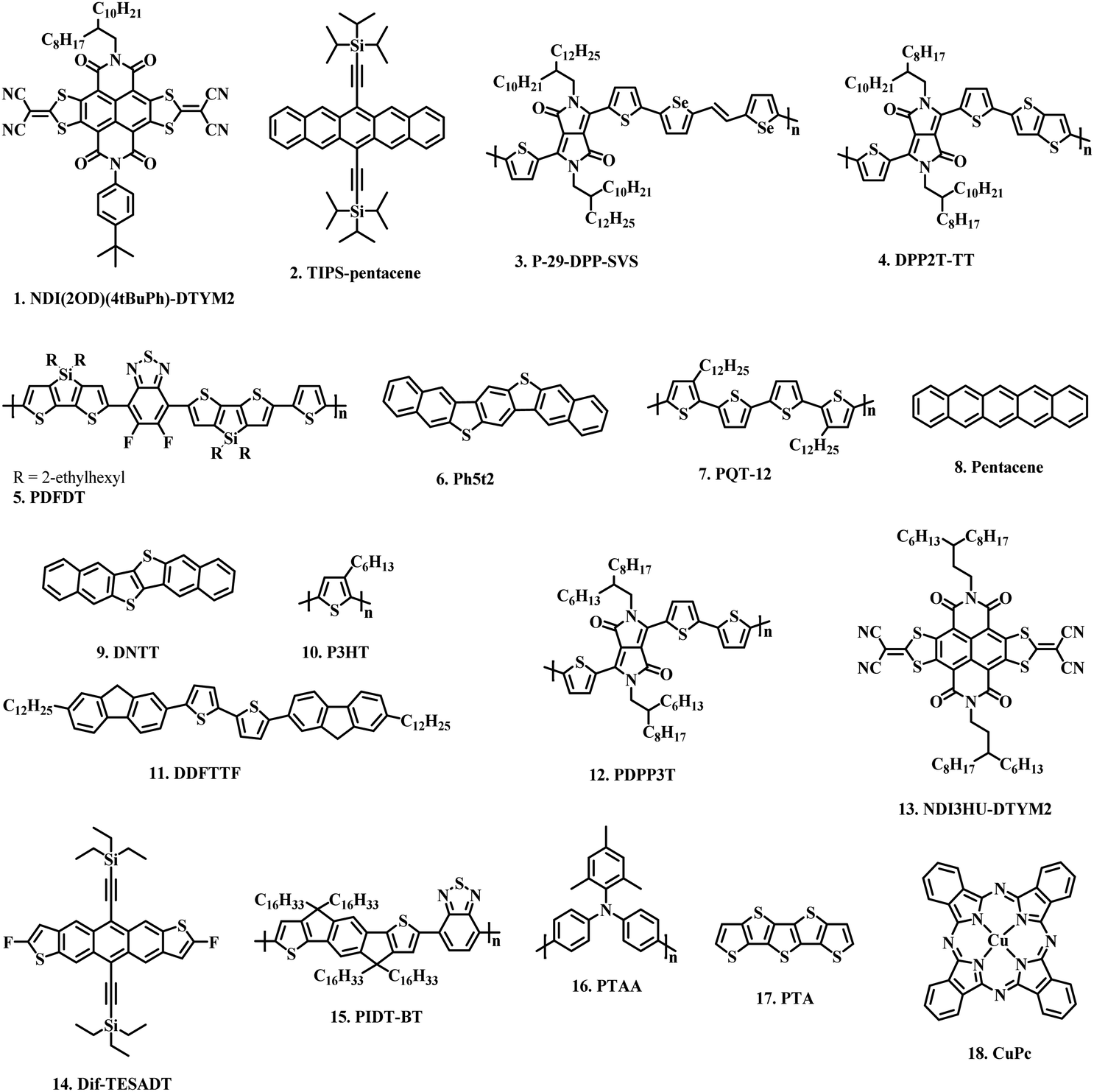 | ||
| Scheme 1 The chemical structures of some organic semiconducting materials used for flexible OFET platforms. | ||
Among different materials, semiconducting polymers and liquid crystals proved to be easy for processing by various techniques such as drop casting, spin coating, and spray coating, whereas small molecules needed complex deposition systems such as thermal evaporators, wherein the deposition rates and substrate temperature must be identified. Due to such controlled deposition parameters, uniformity and high quality of thin films can be achieved in these materials. During gas sensing, these ultrathin films facilitate interaction between the channel region at the insulator/semiconductor (I/S) interface and gas molecules with fewer diffusion-related losses, thus contributing to high sensitivities and specific binding properties. Subsequently, these materials were modified by means of functionalization on the surface of organic semiconductors to open up functional groups to interact with the chemical and bio analytes, or they were doped with other materials to induce properties such as piezoresistivity/piezoelectricity. Furthermore, to achieve an array of sensors, nanolithography is a good patterning solution because of its low complexity in implementation.
The sections below detail different aspects of organic semiconducting materials and their utilization in multiple configurations leading to wearable electronics technology.
1.3 Types of OFET sensors and their working mechanisms
In an OFET, the input signal is voltage, applied to the semiconducting channel via a capacitive structure. This signal, called gate voltage, modulates the current in a narrow portion of the OSC layer (the channel) between two contacts, the source and drain.27 An OFET is typically fabricated in a thin-film multilayered structure (Fig. 1a)—initially developed for amorphous silicon devices28—where the gate capacitor consists of an insulator sandwiched between a metal (gate) and a thin OSC layer. On the OSC side, the source and drain contacts are used for, respectively, injecting and extracting the current flow (ID), which is dependent on both the gate bias (VGS) and the drain voltage (VDS). The conductance of the OSC in the channel area is switched between the on and off states by the gate, which is capacitively coupled through a thin gate insulating layer. The VGS regulates the ID between the source and drain electrodes under a constant VDS.29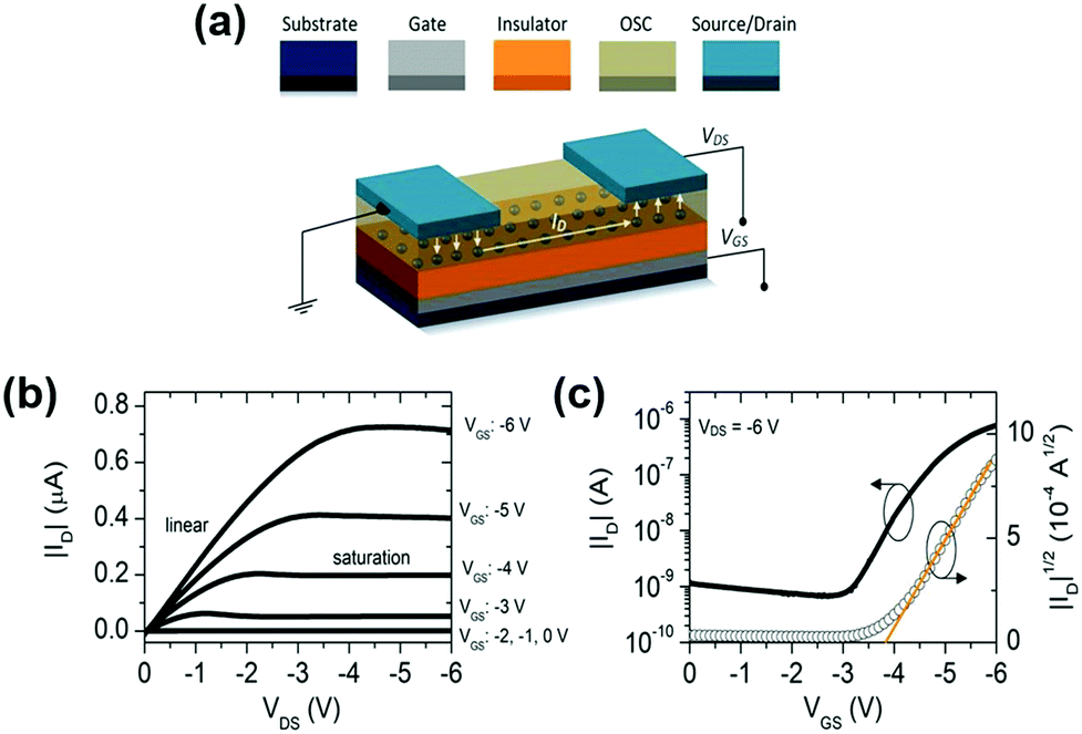 | ||
| Fig. 1 (a) Schematic representation of an OFET device in a typical bottom-gate configuration. Source is, conventionally, the grounded terminal, and the biases VDS and VGS control the charge transport (resulting in electric current ID) injected from the source and extracted at the drain; (b) output characteristics (ID–VDS) and (c) transfer characteristics (ID–VGS) of OFETs based on diketopyrrolopyrrole-naphthalene (PDPP-TNT). (b) and (c) are reprinted with permission from Nawaz et al.30 (copyright 2018, IOP Publishing). | ||
Although transistor electrodes are typically formed from a metal, nonmetallic electrodes (e.g., those made from conducting graphite31 or polymers32,33) have also been reported. The low thickness of the OSC layer is because an OFET does not operate in inversion mode, i.e., the carriers that accumulate in the OSC channel are the same, which usually flow in the semiconductor bulk in the off state. Hence, applying a thick OSC layer would cause a high off state current,34–37 compromising the switching ability of the OFET. The equations quantifying the I–V characteristics of OFETs are normally derived from the model developed for metal–insulator–semiconductor FET devices.38 In the saturation-regime (eqn (1)) and linear regime (eqn (2)), ID is given as:
 | (1) |
 | (2) |
A number of parameters, including μFET, on–off current ratio (Ion/Ioff), and threshold voltage (VT), evaluate the performance of OFET devices. μFET can be defined as the average drift velocity of a charge carrier per unit electric field and decides the processing speed and on-currents of OFETs. Typical μFET values are in the 10−3 to 10−1 cm2 V−1 s−1 range, but they can be greater than 5 cm2 V−1 s−1 for highly ordered OSCs.39–41Ion/Ioff is defined as the ratio of ID at the maximum VGS value (in the accumulation mode) to the ID below VGS − VT (in the depletion mode). It indicates the switching performance of the OFET, and a low off-state current is, in principle, required to ensure a true switching of the device to the off state. To realize complementary circuits having large gains and small power consumption, transistors with large Ion/Ioff are required. VT is the minimum required VGS for the accumulation of free carriers at the I/S interface to form a channel in the OSC layer between the source and drain electrodes. Lower VT helps in reducing the power consumption of the devices and is, therefore, useful in manufacturing portable devices. In principle, VT in OFETs arises because of the traps induced by the non-crystalline structure of OSCs and/or those originating from the surface of the gate insulator layer.
As an example of the electrical characteristics of OFETs, Fig. 1b and c show the I–V curves of devices in which diketopyrrolopyrrole-naphthalene (PDPP-TNT) was used as the OSC.30 The output characteristics (ID–VDS) in Fig. 1b clearly demonstrate the linear and saturation regimes, whereas Fig. 1c shows the transfer characteristics (ID–VGS) and the |ID|1/2–VGS plot, which can be used to easily extract the VT and μFET.
OSCs show susceptibility to noncovalent π-interactions, which allows the detection of external chemical/physical stimuli. This is because the energy supplied in the form of heat/light can result in the modulation of conductivity in the effective channel of OFETs. In this way, OFETs can be efficiently used as sensing devices. Mechanical work, such as pressure, can also alter the output current of OFET devices; such alterations are mainly related to changes in the distribution of charge carriers among molecules in the effective conducting channel.
Tremendous advancements in molecular engineering allow control over the optoelectronic properties of OSCs (electronic energy levels, electrical/optical band gap, etc.) by chemically modifying their structures that can regulate the molecular order and/or morphology.42,43 Consequently, ad hoc-designed OSCs, functionalized with particular recognition receptors or sites, can be used as the sensing layers, providing OFET sensors with the desired capability of the detection of light or environmental molecules (analytes).44,45
Similar to conventional OFET devices, the device geometries of OPTs can be divided into four typical structures: top gate top contact (TGTC), top gate bottom contact (TGBC), bottom gate top contact (BGTC), bottom gate bottom contact (BGBC), as shown in Fig. 2. The light can be illuminated onto the device from the top side (Fig. 2) or the bottom side (not shown here). Depending on the device geometry and direction of light illumination, sufficient transparency of the gate electrode and gate insulator is required so that the light arriving on the OSC layer effectively interacts with the OSC molecules, thereby sufficiently modulating the conductivity in the OFET channel.44
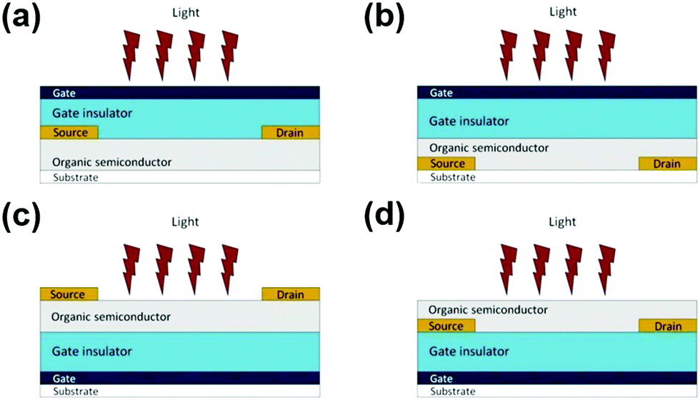 | ||
| Fig. 2 Typical device geometries used for OPTs: (a) TGTC, (b) TGBC, (c) BGTC, and (d) BGBC. | ||
There are typically two operating modes in OPTs, photovoltaic mode and photoconductive mode, both of which are related to photocurrent (Iph) and incident optical power (Popt).48 The photovoltaic mode is dominant when the transistors are operated in the accumulation regime (VGS < VT), whereas the photoconductive mode is dominant when the transistors are operated in the depletion regime (VGS > VT). Among other device parameters, photoresponsivity (R) and photosensitivity (P) are critical for the performance of OPTs. R and P are expressed as:47,48
 | (3) |
 | (4) |
Fig. 3a presents the transfer characteristics of poly(3,3-didodecylquaterthiophene):poly(ethylene oxide) (PQT-12:PEO) nanofiber-based OPTs in darkness and under illumination.49 Similarly, Fig. 3b shows the results of real-time photo-sensing tests of the same devices performed by repeatedly turning the light off and on at 470 and 670 nm, respectively. These devices were fabricated on flexible polyethylene terephthalate (PET) textile substrates and demonstrated an R of 930 mA W−1 and P of 2.76 while exposed to 470 nm wavelength light. The authors also prepared 10 × 10 OPT arrays to be used as flexible image sensors. A red laser source was exposed to the sensor array, and it was observed that the OPTs are able to detect incoming signals at a high resolution. These results highlight the potential of PQT-12:PEO nanofiber OPT arrays to be applied as wearable photo or image sensors.
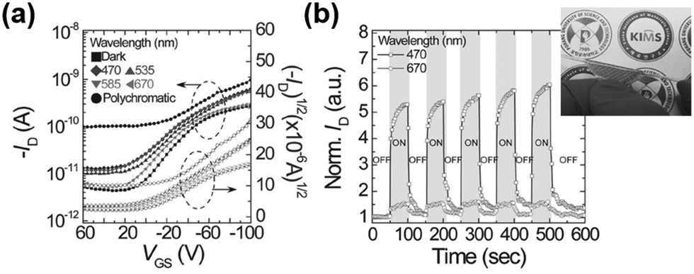 | ||
| Fig. 3 (a) ID–VGS characteristics of PQT-12: PEO nanofiber-based OPTs under light illumination with different wavelengths, and (b) real-time photoresponse while the devices were illuminated using a monochromatic light with two different wavelengths. The inset of (b) shows the photograph of a flexible phototransistor array upon bending at a radius of ∼0.75 mm (reprinted with permission from Lee et al.,49 copyright 2016, Wiley-VCH). | ||
A large number of reports on OPTs stress on improving the optical responsivity by making use of photoactive OSCs, and by performing optimizations on the device structure.50,51 Nevertheless, even after significant advancements, one of the remaining challenges corresponds to distinguishing lights with different wavelengths, which is – in fact – the purpose of the photoreceptor cells in the human eye retina.52 Besides, both effective photodetection and recording of exposure energy are prerequisites for radiation monitoring in the emerging fields of flexible and wearable electronics.53 Recent reports have suggested a viable and straightforward approach to address this issue by integrating the memory functionality in OPT devices.54–58 This results in the preparation of a new class of electronic devices, OPT memories, that integrate photodetection and signal storage in a single device. In this way, the recording of light exposure can be realized by the nonvolatile and cumulative photo-assisted charge trapping.59,60 A promising approach relies on the utilization of molecular photochromics.61 Chen et al. deposited a self-assembled monolayer (SAM) of diarylethene (DAE) photochromic onto the high-κ dielectric hafnium dioxide (HfO2) to realize flexible arrays of pentacene-based low-voltage OPT memories (Fig. 4a).62 The programming and erasing cycles of ID as a function of light intensity are shown in Fig. 4b. Firstly, the device was preset to an initial state by UV light illumination and a gate pulse of −3 V. The programming was then performed by applying 633 nm light with four different levels of light intensity. The initial programming signal caused a sudden increase in ID. In principle, the UV irradiation resulted in the creation of photoexcited electrons, and at the same time, the DAE molecule transformed from its open to closed state via formation of a C–C bond. The latter phenomenon led to π-electron delocalization and decreased the LUMO energy of DAE to −3.22 eV, which is lower than that of pentacene. This resulted in the tunneling of high-energy electrons through the DAE SAM to charge the DAE/HfO2 interface. These trapped electrons provided an additional electric field, thereby leading to an increase in ID. When the light was removed, the stored information was retained for at least 3 hours. This is understandable because the LUMO of DAE in its closed state is lower than that of pentacene, which effectively prevented the trapped electrons at the DAE/HfO2 interface from leaking through the pentacene/DAE interface. In order to recover to the initial state, a gate pulse of −3 V was applied. The authors also analyzed the changes in VT to evaluate the memory window and retention ability of the OPT memories (Fig. 4c). In this case, the memory window was observed to be as large as 50% of the operating voltage, whereas the read-current ratios at VGS = 0 V was as high as 4.4 × 10⁴. Fig. 4d shows a photograph of a flexible OPT memory array (30 × 30 array with 900 memory devices) fabricated on an ITO-coated 5 × 5 cm2 PET substrate. This bendable active-matrix array was utilized to measure the spatial distribution of the incident UV light and to store an analogue image. The resetting and programming was performed in a similar fashion by UV irradiance (365 nm, 100 μW cm−2), while erasure was performed using a gate pulse. The lights were applied in the shape of a butterfly (Fig. 4e), and an evident shape was observed for up to 24 hours after removing the light and applied voltages. The results obtained by Chen et al. show the great potential of flexible OPT memories in practical applications involving environmental monitoring and health care.
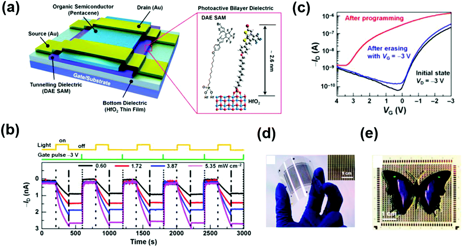 | ||
| Fig. 4 (a) Schematic illustration of pentacene-based OPT memory device consisting of hybrid DAE/HfO2 as the photoactive dielectric layer (molecular structure and real-space model of DAE bonding to HfO2 is shown in the inset); (b) memory characteristics with five representative programming and erasing cycles as a function of light intensity. Programming is performed by 633 nm light illumination with four different intensities, while erasing is performed by a gate pulse of −3 V (VDS = −100 mV and VGS = 0 V); (c) ID × VGS characteristics showing a large memory window and read-current ratio; (d) photograph of a 30 × 30 OPT memory array fabricated on a flexible PET substrate (the inset shows a zoomed-in image of the array); and (e) photograph of a butterfly image stored on top of the flexible memory array (reprinted with permission from Chen et al.,62 copyright 2016, American Chemical Society). | ||
In addition to the three above-mentioned parameters, change in the OSC conductivity can also provide important insight into the sensing performance, which can be measured using an equivalent two-terminal configuration. Indeed, the multi-parametric response feature of OFETs has been reported to yield highly sensitive chemical sensors.73 Similarly, OFET chemical sensors are also known to show enhanced recovery behavior after the sensing activity is completed. Essentially, the charge carriers trapped as a result of the interaction between the analyte and the OFET can be detrapped by applying an opposite VGS.74,75 As a result, the OFET chemical sensors can be repeatedly used.
The sensing mechanism of OFET gas sensors stems from the amenability of OSCs to noncovalent π-interactions. The interaction between the OSC and analyte molecules can occur at the surface of the OSC film or at the grain boundaries in the bulk of the OSC film. At the same time, the analyte molecules can even reach the I/S interface or the metal/OSC interface by percolating through the voids between the OSC grains. The interaction can be detected electrically, intrinsically (via 2D conductivity of the OSC layer), and extrinsically (via VT, μFET, and Ion/Ioff of the OFET device). In certain cases, the analyte exposure induces a shift of VT, which depends on the analyte redox properties.76,77 This behavior corresponds to the sensitivity of VT to carriers injected/extracted from the OSC layer. Since OSCs typically demonstrate an electron-rich conjugated system, they show sensitivity to strong oxidants like nitroaromatic compounds and nitric oxide (NO), which act as electron acceptors and either trap charge carriers or dope the OSC layer. This results in an increase in ID and positive VT shift in p-type OSC materials. Some studies have proposed that the sensing mechanism originates from enhanced accumulation of holes due to oxidation of the OSC77 or from the electron traps owing to the reduction of analyte near the I/S interface.78
In case of the detection of chemicals secreted from the human body, Liu et al. have demonstrated the development of nanoribbon semiconductor-based wearable sensors.79 In these transistors, the source and drain electrodes were modified with glucose oxidase (GOx), chitosan, and single-walled carbon nanotubes (SWCNTs) using inkjet printing for the detection of glucose in human body fluids (tears, saliva, and sweat). The current responses of glucose in artificial human saliva, sweat, and tears are reproduced in Fig. 5a. At first, the baseline current was obtained by submerging the sensors in 0.1× phosphate-buffered saline (PBS). Sequentially, when the electrolyte was changed to human body fluids, a variation in the sensing response was observed (Fig. 5a). This variation was attributed to the pH difference between human body fluids and 0.1× PBS, which resulted in changes in the local electric fields (and eventually the conductance) of the sensors. To test on-body sensing capability, the sensors were attached to an artificial eyeball and an artificial arm (Fig. 5b). After connecting the artificial body parts to the measurement unit, artificial tears spiked with 0.01, 0.1, 1, 10, 100, and 1000 μM glucose were sequentially flowed (Fig. 5c and d). Overall, the authors demonstrated good sensitivity ranging from 0.1 μM to 1 mM. Among other applications, such results highlight the potential of this sensing platform to work as contact lenses for the detection of tear glucose levels.
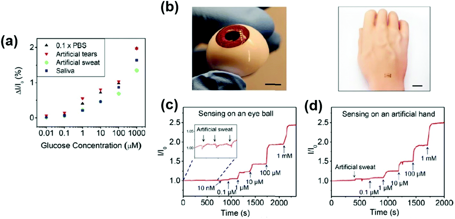 | ||
| Fig. 5 (a) Sensing response of the chitosan and SWNT-modified wearable sensors as a function of glucose concentration in 0.1× PBS, artificial tears, artificial sweat, and saliva; (b) photographs of the sensors attached to an artificial eyeball and an artificial arm, the real-time response of the glucose level in the artificial sweat from the sensor attached in (c) artificial eye ball and (d) artificial hand (reprinted with permission from Liu et al.,79 copyright 2018, American Chemical Society). | ||
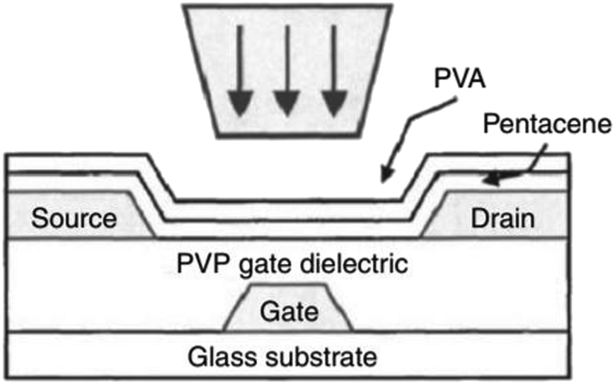 | ||
| Fig. 6 Schematic illustration showing OFETs fabricated on a glass substrate and operating as free-standing pressure sensors (reprinted with permission from Darlinski et al.,81 copyright 2005, American Institute of Physics). | ||
With recent progress regarding OFET pressure sensors, innovative methods have been developed to realize high-performance sensor devices on flexible substrates. For instance, Mannsfeld et al. and Schwartz et al. have reported on flexible pressure-sensor platforms in which the sensitivity of the OFET devices relied on the use of the polydimethylsiloxane (PDMS) gate insulator.10,82 The regularly structured and compressible rubber insulator (PDMS) was the main component leading to high-pressure sensitivity in these devices. In addition, PDMS is well-known for its biomedical amenability with human tissue,83 which made it a favorable choice since the authors were particularly aiming for application in health monitoring and artificial skin. Before applying as the insulator layer in OFET devices, the PDMS thin films were microstructured with pyramid-shaped features (Fig. 7a).10 The resultant PDMS film consisted of voids that enabled the micro-structured surface to elastically deform when external pressure was applied. The external pressures to the OFET sensors were applied and measured with a motorized z-stage in combination with a force gauge, which resulted in an increase in ID. This behavior was explained as a result of the compression of the PDMS layer, which reduced the layer thickness, thereby increasing the gate capacitance and ID. The transfer characteristics of OFET sensors at different pressure loads are reproduced in Fig. 7b. In this case, polyisoindigobithiophene-siloxane (PiI2T-Si) was used as the OSC.82 These flexible sensors revealed a sensitivity of 8.4 kPa−1 and response time of <10 ms. To validate the functionality of the OFET sensors in a bending state, the authors performed radial artery pulse wave measurements, wherein the pressure sensor was attached to the wrist (Fig. 7c). The measurements were conducted in the motorized z-stage while the sensor was operated at constant VGS and VDS. Fig. 7d shows the pulse wave averaged over 16 periods. The first two peaks, P1(t1) and P2(t2), can be used to derive the two most frequently used parameters for arterial stiffness diagnosis (the radial augmentation index AIr = P2/P1, and the time delay between the first and second peaks ΔTDVP = t2 − t184). For the test subject, the authors extracted the AIr and ΔTDVP values as 59% and 155 ms, respectively,82 which are considered healthy for an adult male in his mid-thirties.
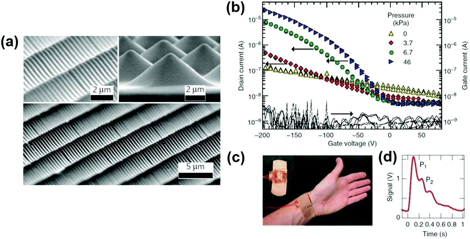 | ||
| Fig. 7 (a) Scanning electron microscopy images of the PDMS thin films. Pyramidal arrays were etched into the faces of Si-wafer molds to form two-dimensional arrays of square pyramids (reprinted with permission from Mannsfeld et al.,10 copyright 2010, Nature); (b) ID–VGS characteristics of flexible OFET sensors as a function of different applied external pressures; (c) an image showing a pressure sensor attached to a person's wrist; and (d) output signal of radial artery pulse measurement averaged from 16 periods. VDS and VGS were −100 V, and ID < 10 mA (reprinted with permission from Schwartz et al.,82 copyright 2010, Nature). | ||
Considering the importance of the development of wearable pressure sensors for emerging artificial intelligence and healthcare systems, Zang et al. developed suspended-gate OFETs.85 The devices were fabricated in the TGBC architecture on flexible PET substrates using poly(diketopyrrolopyrrole-terthiophene) (PDPP3T) as the OSC layer. Strips of polyimide tape were laminated onto the substrates and used as supports to form the suspended gate. The polyimide/Al foil was then transferred to the support and fixed with tapes (Fig. 8a and b). A force gauge and a configurable motorized stand were utilized to apply and measure the external pressure (Fig. 8c). The sensing mechanism in these devices was explained as a result of the deformation of the gate when subjected to an external pressure. This modifies the capacitance of the gate insulator layer as a function of the applied pressure, thereby resulting in a pressure-dependent ID (Fig. 8d and e). Sensitivity in this case is expressed as:
 | (5) |
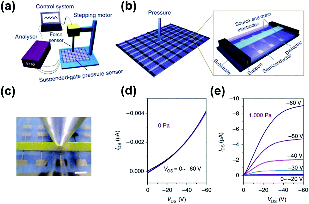 | ||
| Fig. 8 (a) Schematic illustration of the experimental set-up of suspended-gate OFET pressure sensors; (b) an OFET array and magnified view of the device geometry; (c) optical image of a suspended-gate OFET (scale bar corresponds to 1 mm); ID–VDS curves of the transistors recorded at (d) 0 Pa and (e) 1000 Pa (reprinted with permission from Zang et al.,85 copyright 2015, Nature). | ||
Yeo et al. reported on flexible OFET-based pressure sensors by combining a blend of small molecule OSC, 2,8-difluoro-5,11-bis(triethylsilylethynyl)anthradithiophene (diF-TESADT), and poly(methyl methacrylate) (PMMA) with an elastomeric top-gate dielectric, PDMS (Fig. 9a).86 The OSC molecules were observed to vertically segregate and crystallize three-dimensionally at the apex of the PMMA baselines (Fig. 9b). The OFET pressure sensor was essentially prepared with two separate components. A top-gate component consisting of the PDMS elastomeric film was laminated to the bottom component of diF-TESADT:PMMA (Fig. 9c). The preparation of bottom component was performed by thermal deposition of Au source/drain electrodes onto the printed diF-TESADT:PMMA layer. To perform the sensor characterization, the authors used a probe station with a motorized stage to apply precise pressures, while a force gauge was used to measure the pressure-induced deformations, which were reflected by the change in ID (Fig. 9d). The flexible pressure sensors yielded a pressure sensitivity of 1.07 kPa−1, which was largely attributed to the change in capacitance of the gate dielectric layer originated from the pressure applied to the diF-TESADT layer. To demonstrate practical applicability of the flexible OFET sensors, the devices were tested in a prosthetic hand (Fig. 9e) and were utilized for the detection of the wrist artery pulse (Fig. 9f). In the case where the OFET sensor was attached to a prosthetic hand, a water droplet was dropped on top of the OFET sensor. The pressure load of the water droplet brought a change in the output current, and the sensors were found to detect pressures even below 20 Pa. Such results indicate the potential applicability of these sensors in healthcare monitoring and electronic skin applications.
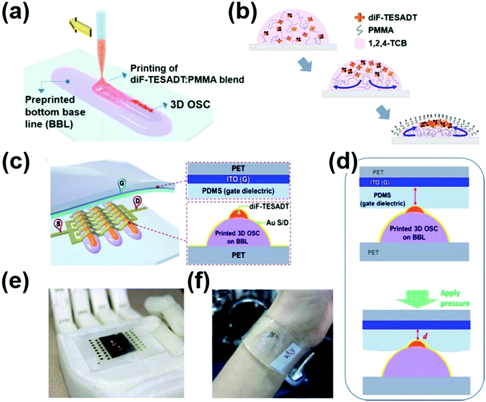 | ||
| Fig. 9 Schematics of (a) the printing of the OSC:polymer (diF-TESADT:PMMA) blend solution on top of the preprinted PMMA baseline; (b) segregation and crystallization of the diF-TESADT molecules assisted by solvent evaporation; (c) flexible OFET pressure sensor in which the bottom component consists of a printed OSC structure, whereas at the top is the gate component consisting of an elastomer gate dielectric; and (d) pressure-sensing mechanism of the OFET sensor; photos (e) and (f) show OFET sensors attached to a prosthetic hand and around the wrist, respectively (reprinted with permission from Yeo et al.,86 copyright 2017, American Chemical Society). | ||
In 2019, Liu et al. fabricated suspended-gate OFET-based pressure sensors on flexible substrates with poly(indacenodithiophene-co-benzothiadiazole) (PIDT-BT) as the OSC.87 The devices consisted of patterned source/drain electrodes, whereas the gate structure (consisting of the gate electrode, the polyelectrolyte gate dielectric, and the polymer semiconductor) was kept at a distance of ∼310 μm from the substrate by using a laminated thin tape (Fig. 10a). The pressure response was obtained by pressing the flexible gate structure of the OFET sensor, which led to the formation of an electrical contact between the polymer semiconductor and the source/drain electrodes. The authors reported high sensitivity values (452.7 kPa−1), while the use of eco-friendly and nontoxic materials allowed the devices to be worn on human skin for spatial pressure mapping (Fig. 10b and c).
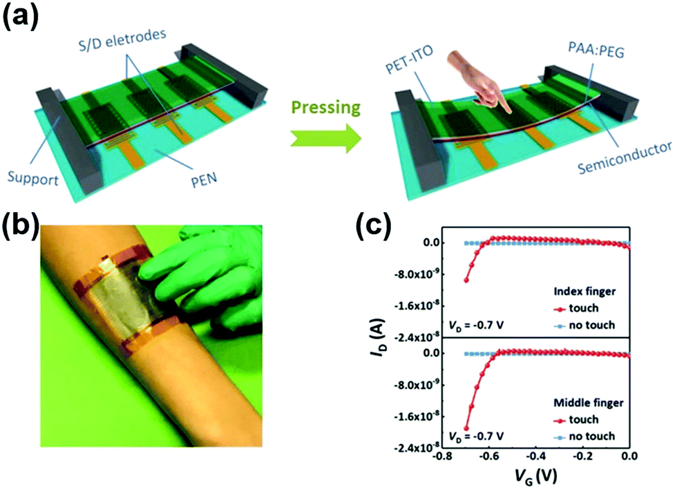 | ||
| Fig. 10 (a) Schematics of the suspended-gate OFET pressure sensors, before and after the pressing of the flexible (suspended) gate structure; (b) photograph of the OFET sensor array affixed to a human arm; and (c) pressure-sensing response of the devices when touched using the index and middle fingers (reprinted with permission from Liu et al.,87 copyright 2019, Wiley-VCH). | ||
In a recent work, Baek et al. reported on OFET-based pressure sensors prepared on a biocompatible flexible parylene C substrate with poly(N-alkyl diketopyrrolo-pyrrole dithienylthieno-[3,2-b]thiophene) (DPP-DTT) as the OSC.88 The pressure-sensing capability of the devices was enabled via preparation of deformable source/drain electrodes by embedding conducting carbon nanotubes on the surface of microstructured PDMS which was integrated on top of a staggered OFET (Fig. 11a). The deformation of the electrodes on the polymer OSC layer modulated the channel geometry and contact resistance, resulting in pressure-dependent ID and a high sensitivity of 18.96 kPa−1 (Fig. 11b and c). In this work, the authors also demonstrated a skin-attachable 5 × 5 proof-of-concept active matrix transistor array (Fig. 11d) which highlights these devices as promising candidates for next-generation wearable electronic skin devices.
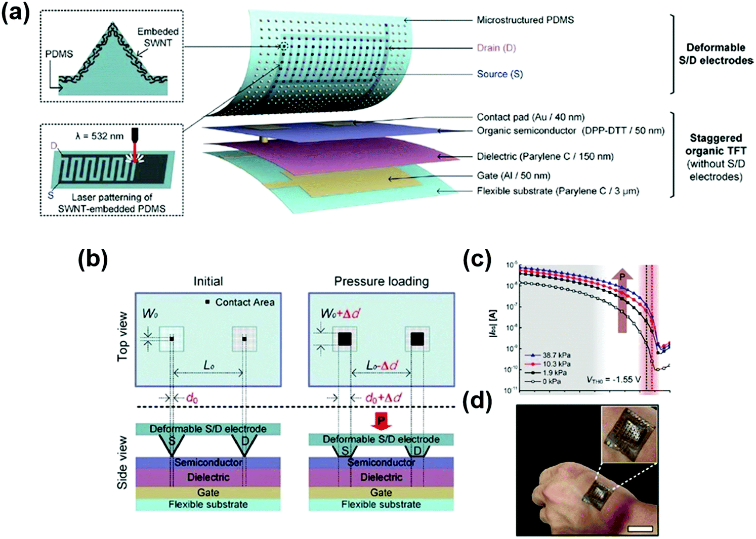 | ||
| Fig. 11 (a) Illustration of an OFET-based flexible pressure sensor consisting of deformable source/drain electrodes integrated on top of a staggered OFET; (b) schematic illustration of OFET pressure sensors demonstrating parameter changes when pressure is applied. Pressure application results in an increase of W from the initial width W0 to W0 + Δd, while L decreases from the initial length L0 to L0 − Δd. This leads to an increase in the channel geometrical parameter, resulting in the pressure dependence of ID; (c) device transfer characteristics as a function of applied pressures; and (d) photograph of the flexible OFET array on the back of a human hand as a proof-of-concept of wearable electronic skin; scale bar corresponds to 2 cm (reprinted with permission from Baek et al.,88 copyright 2019, American Chemical Society). | ||
Song et al. have recently demonstrated a P3HT-based OFET device as a flexible thermal sensor.98 The proposed OFET devices were fabricated using the bottom-gate top-contact configuration, consisting of P3HT as the OSC, PMMA as the gate dielectric, and ITO-coated PEN as the flexible substrate (Fig. 12a). It is important to note that the solvents used for P3HT/PMMA bilayer formation (toluene/chlorobenzene) are not orthogonal to each other. This, in turn, increased the probability of chlorobenzene attacking the P3HT active layer, which can result in the formation of a rough I/S interface. For this reason, the authors observed a positive threshold voltage for the p-type OFET device, as seen in Fig. 12b. Another important characteristic of this device is the deposition of a reasonably thick aluminum-coated flexible PEN substrate on top of the device architecture. This was done to avoid the effect of ambient light on the photosensitive P3HT material.
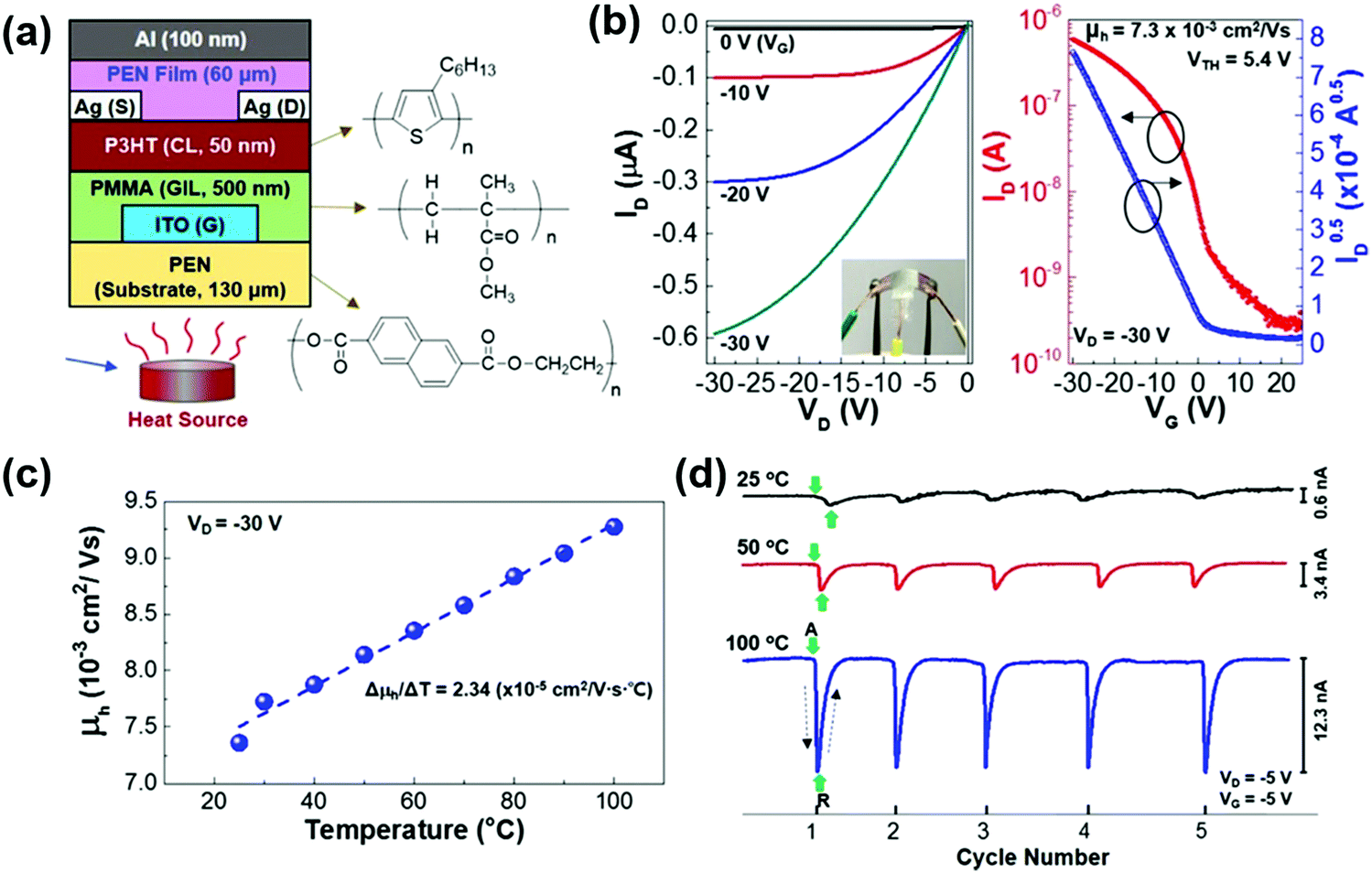 | ||
| Fig. 12 (a) Schematic representation, (b) output and transfer characteristics of the fabricated OFET thermal sensor, (c) relation between charge carrier mobility of the sensor and ambient temperature, (d) drain current response of the sensor for different temperatures (reprinted with permission from Song et al.,98 copyright 2017, American Chemical Society). | ||
The temperature-sensing properties of the proposed device were investigated by measuring transfer and output characteristics at different temperatures ranging between 25 and 100 °C. The ID and μFET showed a gradual and steep increase with temperature (Fig. 12c). Based on these results, the authors investigated the robustness and repeatability of the proposed flexible thermal sensor, the results of which are presented in Fig. 12d. The drain current was observed to increase rapidly and decline relatively more slowly when the temperature source was near and far from the device, respectively. Finally, the as-fabricated flexible thermal sensor was attached to the finger for demonstrating its real-time sensing behavior. Interestingly, the drain current of the sensor remained stable enough while it was attached to the finger. In addition, the instantaneous increase in ID when the sensor was attached to the finger was successfully retrieved after the detachment. Hence, the proposed versatile polymer-based flexible thermal sensor was shown to be robust and mechanically flexible and demonstrated good temperature-sensitive properties. These characteristics make it a good candidate for many artificial skin-related applications.
One of the significant drawbacks of the sensor devices proposed by Song et al. is the requirement of a high operating voltage. This limits the integration of these devices in wearable healthcare-based applications.99–101 Some of the important requirements expected from a thermal sensor in medical industries are high temperature sensitivity with extremely high resolution, mechanical flexibility and robustness, and the capability to continuously monitor the temperature changes for an extended period of time.102–104 Many researchers have addressed these requirements with innovative solutions based on either resistive- or capacitive-based temperature-sensing devices.105–107 However, one of the problems in adapting these available solutions for the target market is related to their inherent poor sensing resolution and the utilization of nonflexible substrates. Furthermore, in addition to the usage of devices based on single parameters such as resistance and capacitance, the concept of employing a multi-parametric OFET approach constitutes an interesting choice.
Mandal et al. have recently reported on flexible OFET sensors in which hexagonal barium titanate nanocrystals (h-BTNC) served as the temperature-sensing layer with PDMS encapsulation.108 The device architecture, as seen in Fig. 13a, was composed of h-BTNC + Al2O3 as the gate dielectric and pentacene as the OSC. It is worth noting that the bilayer dielectric combination was proposed for realizing two important requirements: low operating voltage and low gate leakage current. Interestingly, for the first time, the h-BTNC material was synthesized at low temperatures, of around 60 °C, to achieve nanocrystal morphology, which can significantly reduce the roughness of the surface, thereby improving the quality of the I/S interface. As seen in the transfer characteristics (Fig. 13b), the devices demonstrated a low VT, of about −1.05 V, which was attributed to the combination of h–BTNC and Al2O3 as a gate dielectric material. In addition to this, μFET and Ion/Ioff were found to be around 1.46 cm2 V−1 s−1 and 103, respectively.
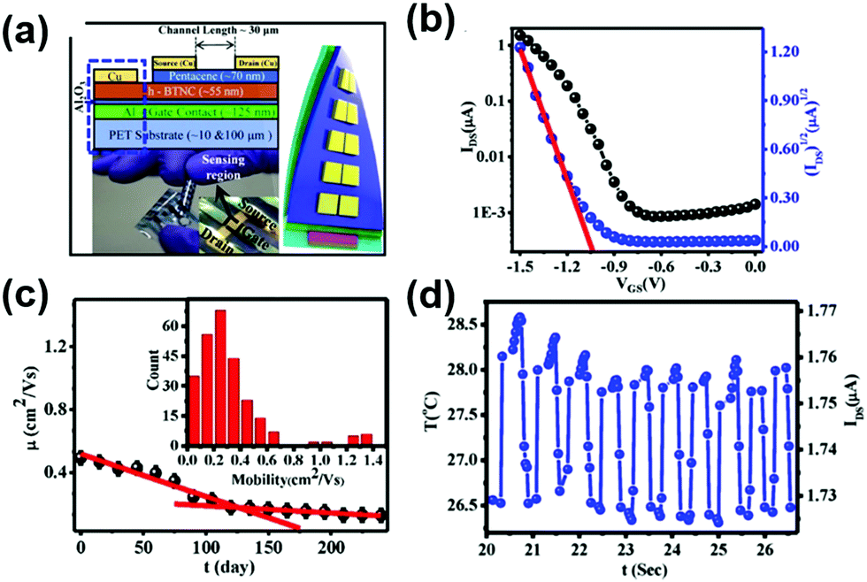 | ||
| Fig. 13 (a) Pictorial representation and (b) transfer characteristics of a pentacene OFET thermal sensor. (c) Stability in terms of charge carrier mobility of the OFET device recorded for more than 200 days. (d) Repeatable thermal sensing performance of the pentacene OFET sensor (reprinted with permission from Mandal et al.,108 copyright 2018, American Chemical Society). | ||
The authors initially performed stability tests on the as-fabricated flexible OFET device. As observed in Fig. 13c, μFET slowly decreased over a testing period of 200 days. To improve the stability, the device was encapsulated by a thin PDMS layer. The real-time response and recovery behavior of the device was tested during inhalation and exhalation of air by a human subject while sensing a change in temperature. The results revealed that the devices were not only able to detect a change in temperature of about 2 °C but also exhibit quick response and recovery characteristics (Fig. 13d). Subsequently, many real-time tests were conducted by exposing the as-fabricated device in water, varied pH, and salt solutions. In all these cases, the as-fabricated device was able to sense the temperature with a high precision of around 4 mK over a narrow range of ambient temperatures ranging between 20 and 50 °C. In summary, Mandal et al. reported a temperature sensor that incorporates the essential features such as low power operation and high precision with quick response and recovery behavior under versatile environmental conditions. These features open various channels and opportunities for these devices to be used for various temperature-sensing applications.
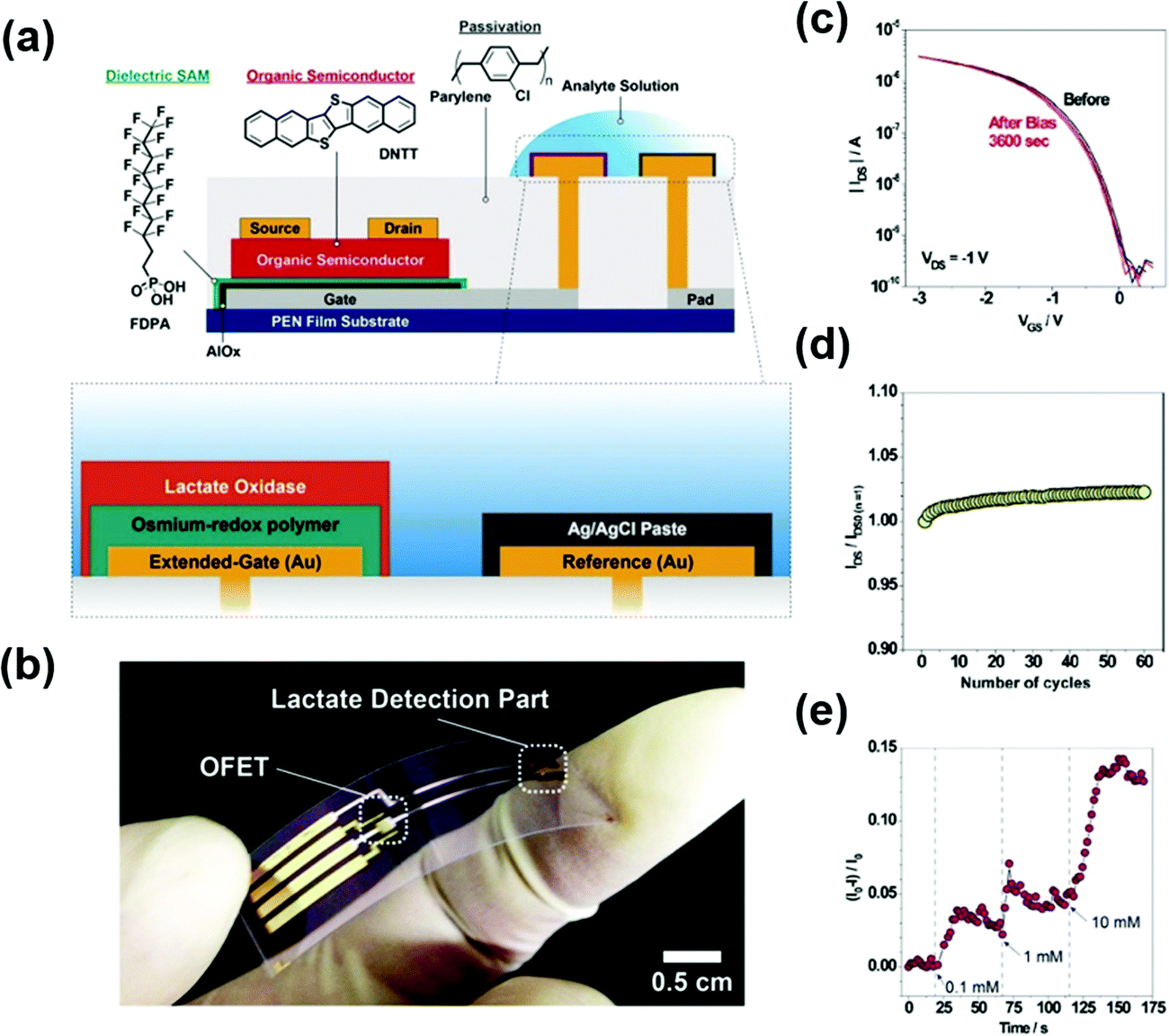 | ||
| Fig. 14 (a) Schematic representation and (b) photograph of a flexible OFET device; effect of bias stress, (c) transfer behavior of one cycle and (d) current response toward 60 cycles; (e) transient drain current response of flexible OFET device toward different lactate concentrations (reprinted with permission from Minamiki et al.,109 copyright 2019, Analytical Sciences). | ||
The whole device architecture consists of a reference electrode (Au/Ag/AgCl) and three vertically stacked layers of Au/osmium-redox polymer/lactate oxidase, connected with each other by the extended electrode. During lactate detection, the target analyte solution was drop-cast on the surface of both reference and extended gate electrodes. When VGS is applied across the reference electrode, the osmium polymer in the extended electrode tends to reduce based on the concentration of lactate. This reduction process results in the formation of positive potential in the gate electrode of the OFET device. This positive gate voltage reduces the majority hole-charge carrier concentration in the DNTT channel region and results in a reduction of ID. Hence, with the change in lactate concentration from 0.1 mM to 10 mM, Minamiki et al. observed that the magnitude of negative relative sensitivity increases with time (Fig. 14e). These results clearly show that the reported sensing device has the capability to sense lactate biomolecules at concentrations as low as 0.1 mM.
It must be noted that in this work, the authors have only used sweat samples for the detection of lactate. Similarly, no significant information was presented regarding the role of parylene-C in the flow cell arrangement. In early reports, researchers have proposed the use of PDMS because of its inherent immunity to many buffers. In the case of parylene-C, a commonly reported issue is related to the formation of pinholes smaller than 1 μm.117 Under such conditions, the sensor platform is vulnerable to non-target analytes and may influence the outcome. Essentially, the pinholes alter the sensitivity of the device by absorbing the anlayte and thereby reducing the limit of detection (LOD) (due to reduced concentration of the actual analyte interacting with the gate electrode).
The sensitivity and detection limit toward lactate are improved by increasing the sensing area and removing the reference electrode part in the extended gate section.110 In addition to this, previously used DNTT material was replaced by a PbTTT-C16 organic semiconductor to improve the device stability and transistor performance. To achieve large scale production, authors have adopted a cost-efficient screen printing technique to print the proposed extended gate based organic field-effect transistors on plastic substrates. The synergistic combination of aluminium/aluminium oxide as gate/gate-dielectric with tetradecylphosphonic acid as an SAM layer played a crucial role in reducing the operating voltage of the device to less than 2 V. The device also exhibited extremely good selectivity toward lactate against other common interferents. This is mainly due to the tailor-made receptor layer composed of both horseshoe peroxidase and osmium redox polymer, and they are functionalized on top of the extended gate. This receptor layer specifically binds with the target lactate species to improve the selectivity of the device. With these specific improvements, the authors were able to augment the LOD to 60 nM which is around 40 nM lower than the previously reported one. Therefore, Minami et al.110 have successfully developed a room-temperature operating, mass-scale production feasible, highly sensitive, selective and extremely flexible lactate sensor.
A step forward for early detection of Parkinson's disease is to develop an on-site monitoring compatible dopamine biosensor. This sensor must be able to detect a wide range of dopamine concentrations ranging from μM to aM depending on different aqueous media. By considering these requirements, for the first time, Jungkyun et al.111 have developed a liquid-ion-gate organic field-effect transistor (LIG-OFET) based dopamine sensor using the enzyme-free approach. In the beginning, the CVD process was used to grow high-quality graphene on top of a flexible PEN substrate. The reason for choosing graphene is to facilitate the immobilization of Pt nanoparticle decorated reduced graphene oxide (Pt-rGO). This immobilized material acts as a receptor layer to specifically bind with the target dopamine analyte. Then, the non-conventional combination of PANI:CSA material was screen printed as the source and drain contacts. The classical buffer solution PBS is deposited on top of the Pt-rGO immobilized substrate to serve as a liquid ion gate dielectric. To evaluate the sensing behavior, the fabricated LIG-OFET was tested toward different dopamine concentrations. As a result, the sensor exhibited a good linear range from 100 aM to 10 nM. Moreover, the sensor was able to selectively detect the target dopamine against other commonly found interferents. High sensing performance on a good flexible substrate of the demonstrated dopamine sensor can be easily integrated to develop wearable and portable sensors.111
Recently, Khan et al.112 have successfully developed a flexible organic field-effect transistor-based biotin sensor. One of the critical challenges faced by the authors is to improve the aqueous stability of the pentacene based OFET device, which is crucial to detect the target biotin analyte. Interestingly, a water-stable CuPc organic semiconductor was deposited on top of an active pentacene layer to serve as a passivation layer. In addition to this, the water stable polymer played an important role in electrostatically attracting but not specifically binding the target biotin molecules from the aqueous medium. Initially, the electrical characteristics of the OFET device was recorded under ambient conditions. The charge carrier mobility of the fabricated organic transistor on a flexible substrate was measured to be around 0.8 cm2 V−1 s−1 at a low operating voltage of around −1 V. Afterwards, the device behavior was tested in the presence of freshly prepared PBS buffer solution. When compared to ambient conditions, there was a slight up-shift in both ON and OFF drain current levels with a small decrease in the charge carrier mobility. Due to the presence of CuPc in between the flow cell and pentacene channel layer, the device was showing exceptional stability in the presence of PBS buffer solution. After this, different concentrations of target biotin molecules were injected into the buffer solution and the corresponding changes in the drain current from the OFET device were recorded. As a result, the CuPc passivated flexible OFET device exhibited excellent sensitivity toward biotin with LOD measured around 200 nM concentration.112 These ultra-flexible sensors can be integrated with the associated circuitry to develop low-cost wearable biosensors. The sensing performances of the above discussed OFET based flexible biosensors are compiled in Table 2. In summary, the authors reported a flexible, reliable, low-power, and highly sensitive lactate sensor that acts as a competitive candidate for noninvasive continuous health monitoring applications.
| Material | Bio-analytes | Sensitivity | Biasing condition | Limit of detection | Media used | Flexibility limit |
|---|---|---|---|---|---|---|
| a V G = gate voltage, VD = drain voltage, Vref = reference voltage, PEN = polyethylene naphthalene. | ||||||
| 9 | Lactate109 | No information | V D = −2.5 V, VGa = −2.5 V | 0.1 mM | PENa | 60 bending cycle tests |
| 5 | Lactate110 | No information | V D = −1 V, VG = −1 V | 66 nM | PEN | No information |
| 11 | Dopamine111 | 1% nM−1 | V D = 1 V, VG = 10 mV | 100 am | PEN | No information |
| 8 | Biotin112 | 6 nA μM−1 | V D = −0.5 V, VG = −1 V | 200 nM | Polyimide | No information |
2. Semiconducting materials for flexible OFET sensors
Different OSCs are in use for OFET devices but for the purpose of flexibility these materials need to have various physical and electrical advantages to serve different applications. For example, they need to be sensitive enough for analytes even under strain conditions, rigorous application of external forces should not alter the dynamics in sensing and they should recuperate at faster rates in case of any deformation. In the following section, we have described the importance of OSC materials in different sensor applications. Typically, tuning material's properties not only brings more specificity and improved shelf-life but also can eventually help to reduce multi-faceted problems at the system level like power consumption and analyte classification.2.1 Semiconducting materials for chemical sensors
| Materials | Analyte | Sensitivity | Voltage bias condition | Limit of detection (ppm) | Flexibility limit |
|---|---|---|---|---|---|
| a I DS: drain current; RC: channel resistance. | |||||
| 1 | NH3118 | I DS : 6.25%@10 ppm | V GS = 60 V, VDS = 60 V | 10 | No information |
| 2 | NH3119 | I DS: 25%@100 ppm | V GS = −40 V, VDS = −40 V | 10 | No information |
| 3 | NH3120 | R C : 100%@0–1000 ppm | V GS = −5 V, VDS = −5 V | 29 | 8.3 mm bending radius |
| 4 | NH3121 | I DS: 82%@10 ppm | V GS = −5 V, VDS = −5 V | 10 | No information |
| 5 | NH3122 | I DS: 2.8%@1 ppm | V GS = −5 V, VDS = −5 V | 1 | No information |
| 6 | H2S123 | I DS: 400% [tensile stress]@1 ppm | No information | 1 | 7 mm tensile and 15 mm compressive stress states |
One such dangerous gas is ammonia; so Zhang et al.118 have proposed highly transparent and flexible n-channel OFET-based devices for ammonia-sensing applications. They initially considered OSCs such as 13, 1, PBTTT-C12 (P1), and 10 (with reference to materials mentioned in Table 1) and investigated their electrical characteristics for different thicknesses or numbers of molecular layers. As depicted in Fig. 15a, the μFET of n-type material 13 stayed stable for the thickness ranging between a number of 10 and 4 molecular layers. However, the μFET rapidly decreased for polymer thickness less than 4 molecular layers. This sudden decrease in μFET may be due to the presence of trap states along the I/S interface region. Unlike material 13, by reducing the thickness from 60 nm to 4 nm, the μFET of n-type polymer P2 remains constant. Therefore, to achieve good transistor performance, an ultrathin polymer layer is preferred, which, in turn, reduces the surface roughness and supports the formation of a large grain size.
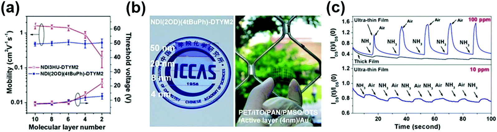 | ||
| Fig. 15 (a) Relationship between transistor parameters and the thickness of the active layers; (b) demonstrating the transparent properties of the as-fabricated device; (c) ammonia-sensing properties of thick and ultrathin film-based devices (reprinted with permission from Zhang et al.,118 copyright 2013, Wiley-VCH). | ||
Fig. 15b shows the flexible and transparent ambipolar OFET device fabricated by depositing 4 nm of ultrathin n-type P1 polymer on the surface of 50 nm thick p-channel pentacene with PMSQ polymer as the gate dielectric layer. It is worth noting that the purpose of using an ultrathin layer of polymer is to enhance the interaction of target analytes with the polymer active channel layer at the I/S interface region. To emphasize this, ammonia gas-sensing studies were conducted for different thicknesses of P2 polymer active layers, as shown in Fig. 15c. In the case of an ultrathin film device, the sensitivity toward 100 ppm of ammonia was around one order of magnitude higher than the response of the thick film-based device. Moreover, comparatively, the ultrathin film-based device was able to sense ammonia down to a range of 10 ppm. Many researchers have reported that the utilization of ultrathin organic films is one of the most important requirements for achieving good sensitivities for various gas molecules.126–129 Therefore, it is clear that the sensitivity is solely based on the architecture of the device and organic film morphology.
One of the most important issues in the proposed work of Zhang et al. is the use of the spin-coating technique, which has the potential to damage the surface and increase the roughness of some of the low-cost and commonly used polymer dielectric layers.130 This can, in turn, affect the performance of the as-fabricated device. Based on this perspective, Yu et al. employed a spray-coating technique to deposit an ultrathin layer of high-mobility TIPS-pentacene material on a commonly used PMMA gate dielectric material (Fig. 16a).119 From the electrical characteristics (Fig. 16b and c), the as-deposited TIPS-pentacene devices showed p-type behavior with μFET and VT of around 0.068 cm2 V−1 s−1 and −4.2 V, respectively. By increasing the ammonia concentration from 0 to 100 ppm, the drain saturation current was reduced by four times, and VT shifted negatively from −5 V to −20 V (Fig. 16d and e). This is because when ammonia interacts with an active layer, the incoming analyte tends to form charge trap sites, which significantly reduces the charge carrier concentration and mobility at the PMMA/TIPS–pentacene interface. Under 100 ppm of ammonia exposure, the response and recovery times of the sensor were around 10 and 240 s, respectively. Subsequently, transistor and sensing behavior of the devices was tested on Arylite/ZITO-based flexible plastic substrates. The μFET of the as-fabricated flexible device was measured to be around 0.0062 cm2 V−1 s−1. Moreover, the ammonia-sensing performance of the flexible device coincides with the response of the glass-based device (Fig. 16f). The photo-image of the as-fabricated device is presented in Fig. 16g. These results clearly show that the TIPS-pentacene-based OFET device is mechanically stable and has good sensitivity toward ammonia gas.
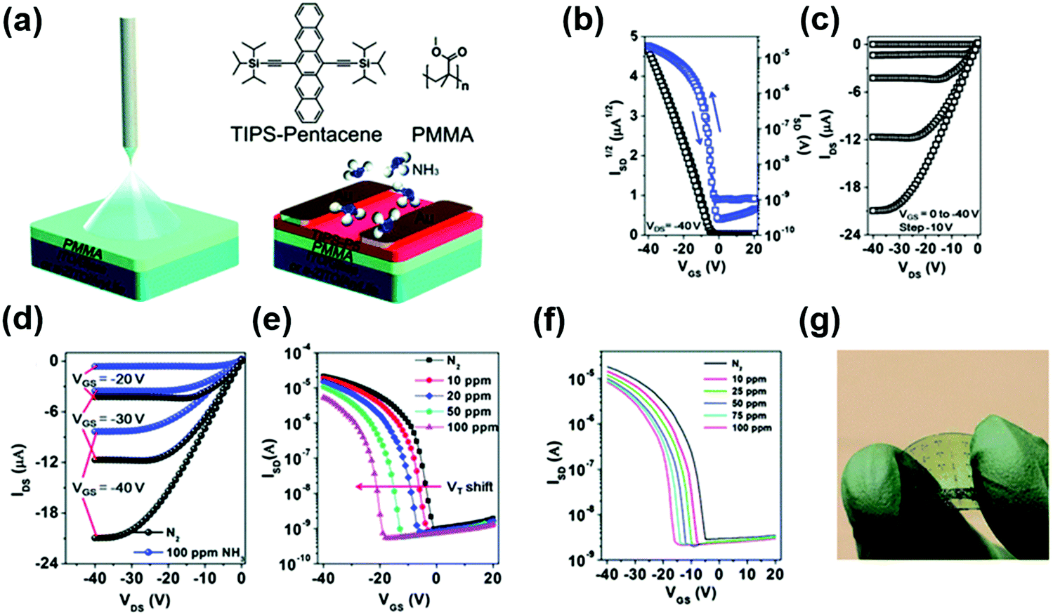 | ||
| Fig. 16 (a) Schematic representation; (b and c) electrical characteristics; (d and e) ammonia-sensing behavior of the as-fabricated TIPS-pentacene on a glass substrate; and (f and g) ammonia-sensing behavior of the same device on a flexible substrate (reprinted with permission from Yu et al.,119 copyright 2013, Royal Society of Chemistry). | ||
Important properties of OSCs, such as low-temperature processing, high mobility, and high environmental stability, are some of the ideal requirements for achieving reliable OFET-based gas sensors.120 To satisfy these requirements, Ryu et al. used P-29-DPP-SVS, a donor–acceptor (DA) conjugated polymer, as the active sensing layer in an as-fabricated OFET (Fig. 17a).120 The transistor and gas-sensing properties of the reported polymer were investigated by using two different device geometries (TGBC and BGTC, respectively) on two different substrates, namely glass and flexible PEN substrates. The μFET values were measured to be around 3.48 and 2.98 cm2 V−1 s−1 on glass and flexible substrates, respectively. One of the important characteristics observed by the authors was the stability of these devices in both N2 and air ambient environments (Fig. 17b). A reasonable explanation lies in the utilization of the top-gate geometry, which potentially served as an encapsulation layer, protecting the polymer OSC from environmental effects.32,131–133 Subsequently, fabrication of devices on flexible PEN substrates was considered for investigating their mechanical stability. As seen in Fig. 17c, some of the parameters such as VT and μFET remained constant even after 1200 bending sequences (bending radius: 8.3 mm). This clearly shows that the reported device is a good candidate for flexible platform-based applications.
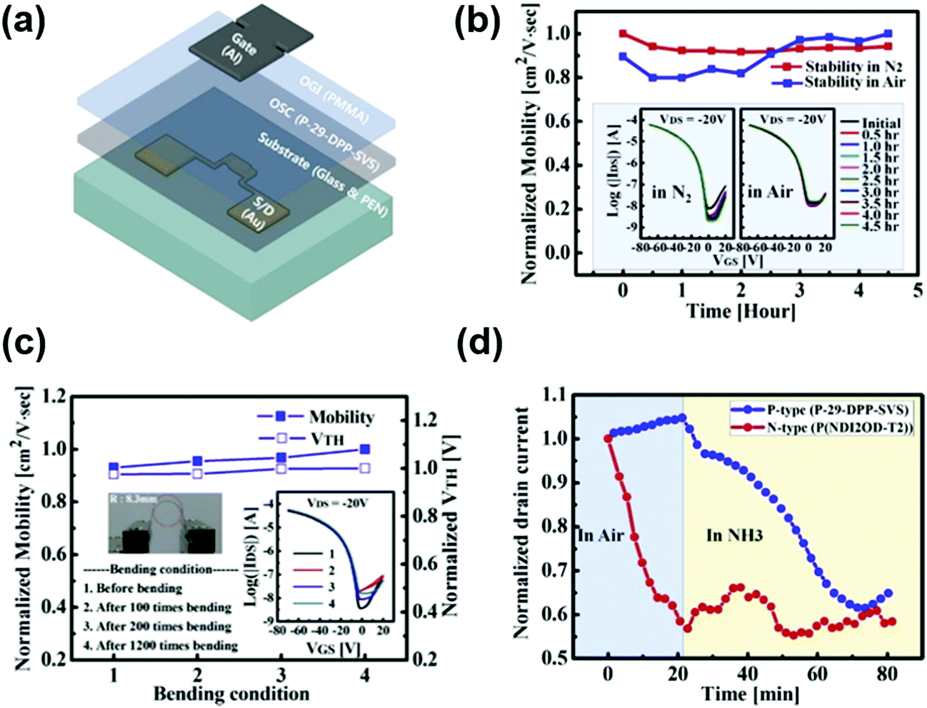 | ||
| Fig. 17 (a) Schematic representation of a P-29-DPP-SVS-based OFET device. Relationship between the normalized mobility and the effect of (b) air and N2 ambient, and (c) bending radius of the flexible OFET device. (d) Ammonia-sensing behavior of both p-type P-29-DPP-SVS and n-type (P(NDI2OD-T2)) materials (reprinted with permission from Ryu et al.,120 copyright 2015, Elsevier B.V.). | ||
To test the gas-sensing properties of the P-29-DPP-SVS-based OFETs (Fig. 17d), the devices were exposed to ammonia. It was observed that an increase in the concentration of ammonia from 29 to 1000 ppm results in a decrease of ID and a negative shift of VT. The sensing mechanism was further tested under ammonia exposure for both p-type P-29-DPP-SVS and n-type P(NDI2OD-T2) materials. The results revealed an abrupt decrease and a gradual increase in ID for the p-type and n-type devices, respectively, which was attributed to the electron donor doping effect of ammonia.
Compared to the spin-coating method, deposition techniques with added advantages such as compatibility with industrial processing routes, large-scale production, and precise film thickness control are required to fabricate arrays of polymer-based flexible and transparent OFET architectures.101,134 To fulfill this requirement, Khim et al.135 reported the fabrication of ultrathin, uniform, and highly transparent devices based on p-channel (DPPT-TT) and n-channel (P(NDI2OD-T2))-based polymers. Devices were fabricated on flexible substrates with the help of a homemade bar coating solution-processed method. Primarily, the charge transport behavior of the reported polymers was investigated by embedding them as an active semiconductor layer in TGBC geometry. The results showed that the maximum μFET of DPPT-TT and P(NDI2OD-T2) is around 1.78 and 0.34 cm2 V−1 s−1, respectively, which decreased with their thickness. In contrast, the VT of both polymers exhibited positive shifts by reducing their thickness. In addition, a BGBC device geometry on a PEN substrate was adapted for studying the gas-sensing properties of a DPPT-TT polymer. This study was performed by exposing the DPPT-TT-based device to ammonia (10 ppm), ethanol (1000 ppm), and ethylene (1000 ppm). In this case, the DPPT-TT polymer having a thickness of around 2 nm showed sensitivity toward ammonia of about 80%, which was 4 and 8 times greater than the respective responses of 5 and 12 nm-thick polymer-based devices. Nevertheless, one of the main issues in employing ultrathin polymers for sensing purposes is the poor stability of the OSCs.135 Due to this issue, ID showed a rapid decay over a short span of time when compared to their thick polymer counterparts.135 Moreover, the proposed ultrathin device also tends to show significant sensing responses toward ethylene and ethanol vapors.
Notably, the devices reported above have two important setbacks—namely, low ambient stability and low selectivity toward target ammonia analyte. Hence, further development in this area would require careful optimization of the polymer film thickness without compromising the device performance.135 This could eventually lead to a more robust sensing platform for ammonia and ethylene sensing, whereas the latter problem may be solved by employing fluorinated π-conjugated polymers.136–138 One solution was proposed by Benjamin et al., who reported on highly sensitive ammonia sensors.121 The OFET sensors were prepared in BGTC geometry and were composed of an ultrathin PDFDT polymer as the active layer (Fig. 18a).
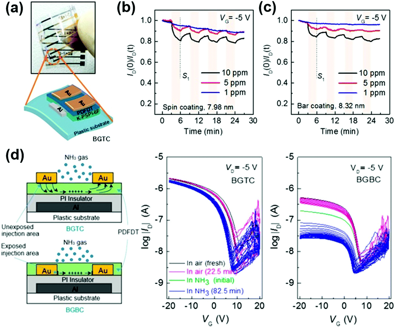 | ||
| Fig. 18 (a) Schematic representation of PDFDT OFET sensor arrays on flexible substrates; (b) spin-coated and (c) bar-coated OFET sensing behavior to 10, 5, and 1 ppm ammonia gas; (d) ammonia-sensing mechanism and associated transfer behavior in BGTC and BGBC device geometry (reprinted with permission from Yawson et al.,121 copyright 2017, American Chemical Society). | ||
To augment the analyte–semiconductor channel interaction, ultrathin (<9 nm) poly(4-(4,4-bis(2-ethylhexyl)-4H-silolo[3,2-b:4,5-b′]dithiophen-2-yl)-7-(4,4-bis(2-ethylhexyl)-6-(thiophen-2-yl)-4H-silolo[3,2-b:4,5-b′]dithiophen-2-yl)-5,6-difluorobenzo[c][1,2,5]thiadiazole) (PDFDT) active polymer was deposited with the help of both bar-coating and spin-coating techniques. The ammonia gas-sensing properties of the reported device were investigated at different exposure levels (10, 5, and 1 ppm). When compared to its bar-coating counterpart, the spin-coating-based OFET device showed good sensitivity of around 13, 5, and 1% for 10, 5, and 1 ppm, respectively (Fig. 18b and c). Under ammonia exposure, the density of the dominant hole charge carrier in the PDFDT OSC channel reduced, which affected the flow of the drain current. To understand the interaction between ammonia and PDFDT molecules, density functional theory (DFT) calculations were performed in three different modes of operations. The results showed that both hydrogen and electrostatic interactions were the two dominant effects that resulted in the sensing of ammonia gas vapors at low concentrations.
To understand the effect of different device architectures on sensing performance, two devices were fabricated in BGBC and BGTC geometries. As shown in Fig. 18d, the former device geometry showed a significant sensing response toward ammonia gas exposure when compared to its BGTC counterpart. This is because in the case of BGBC geometry, the area of the semiconductor exposed to the ammonia gas is relatively high. This, in turn, increased the trap density and, hence, the density of hole charge carriers at the I/S interface, influenced by the physically adsorbed ammonia gas molecules.
One of the drawbacks of most of the flexible gas-sensor reports that have been discussed is the absence of data regarding the effect of mechanical flexibility on gas-sensing performance.118–121,135 This problem stands as a barrier for the commercial market in understanding the capability of a given flexible device for real-time sensing applications. To overcome this obstacle, Tang et al. studied the mechanical deformation effects of a dinaphtho[3,4-d:3′,4′-d′]benzo[1,2-b:4,5-b′]dithiophene (Ph5T2) single-crystal-based OFET device under H2S gas exposure.122 The devices were fabricated on PET substrates, while the single crystalline Ph5T2 layer was deposited on the surface of PMMA gate dielectric with the help of the vapor-transport method. The authors justified the use of Ph5T2 for testing gas-sensing properties because of its good electrical characteristics and ultrathin film formation capability with the added advantages of appreciable mechanical and environmental stability.139,140 The reported device architecture is presented in Fig. 19a and b. In the first stage of investigation, the effect of substrate bending on the electrical characteristics of the OFET device was studied. This study showed that the drain saturation current decreased steeply and slowly ramped up under tensile and compressive states, respectively. Under non-stress conditions, the μFET of the device was measured to be around 0.07 cm2 V−1 s−1, which is about seven times greater and four times smaller than the tensile and compressive counterparts.
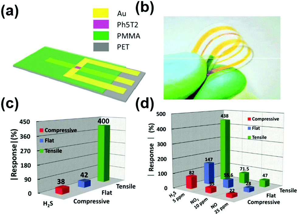 | ||
| Fig. 19 (a) Schematic representation and (b) camera image of a Ph5T2 flexible OFET device. Effect of compressive, flat, and tensile stress on the response of the flexible OFET in the presence of (c) 1 ppm H2S and (d) 5 ppm H2S, 10 ppm NO2, and 25 ppm NO (reprinted with permission from Tang et al.,122 copyright 2017, IEEE). | ||
Subsequently, the effect of stress conditions on the device's gas-sensing behavior under exposure of H2S gas was investigated. As shown in Fig. 19c, under 1 ppm H2S gas exposure, the device with high tensile stress exhibited good sensitivity of around 400%, which is approximately 10 times greater than the response from compressive and non-stress state conditions. Moreover, the authors also performed a selectivity study by exposing the testing device to three different gases: NO (25 ppm), NO2 (10 ppm), and H2S (5 ppm). Among these, the device responded to H2S with a sensitivity of around 438% under compressive stress conditions (Fig. 19d). The study by Tang et al. clearly depicts the effect of different stress conditions on the sensitivity of the device to H2S gas. The proposed device showed good mechanical flexibility, high sensitivity, and selective H2S gas-sensing capability. These features highlight the suitability of the reported device for future flexible and wearable electronics applications.
To improve the sensitivity and selectivity of target analytes, one of the important factors to account for is the efficient interaction between the analyte and OSC materials. This interaction mechanism is mainly guided by two important parameters: the aspect ratio of the sensing layer and the availability of functional groups for selective interaction with target analytes.141,142 These requirements triggered Young et al. to propose the combination of nanostructure and surface functionalization strategy for augmenting the sensing performance of flexible and transparent sensing devices.123 Formation of nanofibers in a polymer solution may be considered a challenging task, especially with an electro-spin deposition technique.
Thus, Young et al. started with the investigation of sensing capability by using a synergistic combination of PQT-12 nanofibers and polyethylene oxide (PEO). In this work, OTS-modified Si/SiO2 substrates were utilized, and Au source/drain contacts were patterned on top using conventional photolithography. Subsequently, an organic polymer solution was prepared by blending PQT-12, calix[8]arene and poly(ε-caprolactone) molecules, which served as the active material, functionalizing agent, and high molecular weight polymers, respectively. The resultant solution was carefully electro-spun, with optimized parameters on the surface of the as-fabricated device to obtain PQT-12-based nanofibers. The schematic representation and the optical micrograph of the as-fabricated device are presented in Fig. 20a and b. The electrical properties of both p-type PQT-12 and PQT-12/calix[8]arene OSC-based devices were performed and tabulated. In principle, the nanofibers protrude out of the surface of the sensor device and can readily interact with the incoming analytes. The calix[8]arene-functionalized device exhibited higher hole mobility and VT when compared to its pristine PQT-12 counterpart.
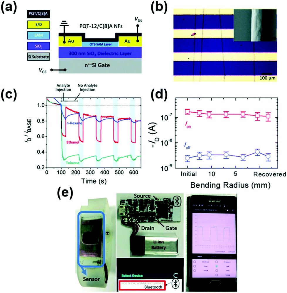 | ||
| Fig. 20 (a) Schematic illustration of a PQT-12/C[8]A NF-based OFET device; (b) optical image along with SEM (inset) image of nanofibers; (c) transient response toward n-hexane, ethanol, and toluene vapors; (d) effect of bending radius on both “off” and “on” current of the device; (e) real-time demonstration of the OFET sensor for an IoT-based monitoring system (reprinted with permission from Kweon et al.,123 copyright 2019, Royal Society of Chemistry). | ||
The chemical-sensing properties of PQT-12/calix[8]arene were tested under different electron-donating VOCs such as ethanol, n-hexane, and toluene. Toward these VOCs, the device exhibited a negative relative sensitivity trend, as shown in Fig. 20c. This is because, under VOC exposure, these electron-donating vapors tend to trap the majority hole-charge carriers from the active OSC. Consequently, ID is reduced, which contributes to negative relative sensitivity. With the addition of calix[8]arene molecules, the host PQT-12 materials tend to show good sensitivity for ethanol and toluene of around 192% and 229%, respectively, when compared to counterpart n-hexane. This response can be attributed to the improved physical adsorption of the exposed analytes on the surface of calix[8]arene receptor layers, which significantly affected the ID of the as-fabricated device. Subsequently, the PQT-12-based flexible sensing device was fabricated, and its electrical behavior was tested as a function of the bending radius. As seen in Fig. 20d, by increasing the bending radius from 0 to 12.5 mm and then releasing it back to the normal condition, Ion and Ioff remain constant at 10−7 A and 10−9 A, respectively. Moreover, the effect of bending was found to be negligible on the chemical-sensing response of the modified PQT-12 flexible sensor device. This clearly shows that the reported flexible device exhibits not only good mechanical stability but also exceptional operational stability.
In addition, the authors also demonstrated the use of a flexible sensor for ethanol detection and wireless transferring of data to a smartphone with the help of customizable data processing board (Fig. 20e). However, one of the drawbacks of this work is related to the use of SiO2 as the gate dielectric, which significantly increased the device's operating voltage. This would eventually require frequent battery recharge as the whole setup is based on a Li-ion battery. One viable solution is the utilization of a high-κ dielectric that guarantees low power consumption. Nevertheless, the reported flexible device is a good product to match the current requirement in smart sensing applications. The reported sensor has some of the important properties—namely, good stability under ambient conditions and high chemical-sensing capability—which makes it a suitable candidate for IoT smart-sensing applications.
The common sensing mechanism proposed in the majority of the reported literature follows three important steps: (1) physical adsorption of humidity analyte at the interface between air and the organic layer, (2) diffusion of analyte molecules from the OSC surface to the I/S interface, and (3) the modulation of charge carrier density at the I/S interface and consequent variation of the OFET electrical behavior. However, the sensitivity of the device mainly depends on the efficiency of the second step in the proposed mechanism. To improve this efficiency, the utilization of ultrathin OSC films has been suggested to augment the interaction between the analyte and the OFET I/S interface. Nevertheless, the main bottleneck in the proposed solution is related to poor mechanical stability.169,170 To overcome this, Park et al. reported ultrasensitive humidity sensors with the help of a unique sensing mechanism based on an analyte-induced doping phenomenon.171 In this work, the authors considered Si/SiO2 substrates for the device fabrication process. The unique part of this study was the inclusion of a polyelectrolyte layer whose electrical conductivity changed with respect to the ambient humidity condition.
The important aspect addressed by the authors is related to the diffusion of analytes into the sensing medium.171 They adopted a supporting material into the system that can enhance the diffusion of the analyte to the I/S interface. The dielectric polyelectrolyte layer was spin-coated and successfully sandwiched between the top OSC layer of pentacene and the bottom dielectric layer of SiO2. The transistor behavior of the as-fabricated device was tested under different humidity conditions. It was observed that the response improves due to the enhancement of ion migration in the polyelectrolyte upon absorption of moisture. The transfer characteristics showed a linear increase in ID from 10−11 to 10−4 when the humidity was increased from 0 to18% (Fig. 21a). This increase in ID was attributed to the release of negative chlorine ions triggered by humidity. Due to the electrostatic effect, these free chlorine ions tend to attract the majority of hole-charge carriers at the polymer/polyelectrolyte interface. As a result, the hole-charge carriers facilitate the increase in ID, as shown in Fig. 21b. In addition to this, as shown in Fig. 21c, the as-fabricated device showed good repeatability and reliable performance with exceptional response (10 s) and recovery (40 s) times.
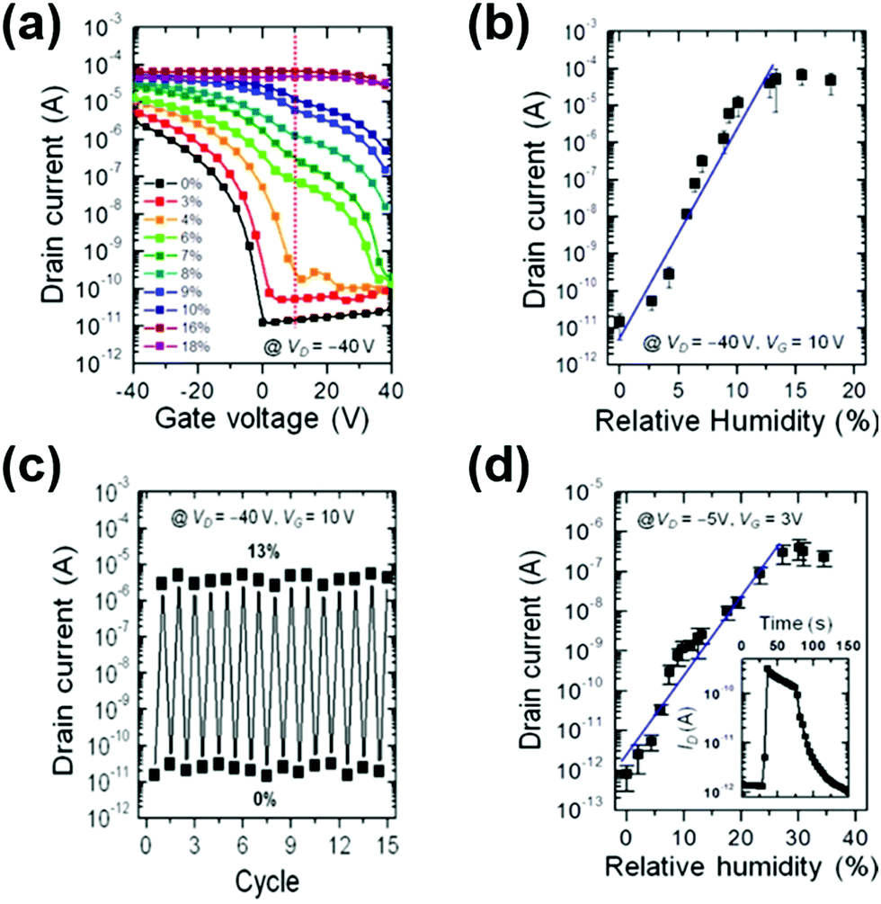 | ||
| Fig. 21 (a) Effect of different humidity levels on the transfer behavior of an OFET device. At VD = −40 V and VG = 10 V, (b) relationship between the device drain current and humidity, and (c) repeatable behavior of the device toward 13% humidity. (d) Flexible OFET device behavior and (inset) transient response toward different humidity levels at VD = −5 V and VG = 3 V (reprinted with permission from Park et al.,171 copyright 2013, American Chemical Society). | ||
To develop a transparent and flexible sensor, the rigid Si/SiO2 substrate was replaced by a flexible PEN substrate. In this case, alumina was employed as the gate dielectric, whereas graphene was used as the top source/drain contact electrode. Because of the use of high-κ dielectric materials, the operating voltage of the devices drastically decreased by ten times without compromising the unique sensing performance. An interesting feature is the sensing window extension by impeding the Cl− ions into the polyelectrolyte, which reduces the humidity interaction. Furthermore, the authors observed an abrupt increase in ID at low humidity levels. In the case of alumina dielectric, the sensor window doubled as compared to SiO2, and the current increased continuously up to a relative humidity of 30% as shown in Fig. 21d.
The integration of microelectromechanical systems (MEMS) with the standard OFET model is another novel strategy for augmenting the performance of a humidity-sensing device.172,173 For instance, Thuau et al. have proposed a novel combination of organic MEMS cantilever and OFET-based transducer architecture as a humidity sensor.174 Poling of the dielectric layer was achieved with the application of an electric field, which essentially helps in inducing the piezoelectric nature into the gate dielectric. Polarized devices can exhibit high sensitivity since this doubles the ID current in comparison to a nonpolarized dielectric. The device's working mechanism is similar to a cantiFET172 in that when there is a mechanical load, the cantilever bends, and the change in the piezoelectric property of the gate dielectric brings a change of the semiconducting channel.
The schematic and SEM images of the as-fabricated device presented by Thuau et al. are shown in Fig. 22a and b, respectively. The authors prepared a humidity-sensitive hydrogel layer and deposited it on the surface of the microcantilever. Under humidity exposure, the hydrogel layer initially tends to swell and develop strain on the surface of the cantilever, and the cantilever tends to oscillate due to the bilayer. This oscillation influences the piezoelectric gate dielectric, P(VDF-TrFE)/PVT polymer, to induce the polarization effect. This effect, in turn, influences the transistor channel properties and, hence, the drain current. As a result, the sensitivity and limit of detection (LOD) of the proposed humidity sensor was around 7500 ppm per % RH and 0.2% RH, respectively, as shown in Fig. 22c. Moreover, the reported humidity sensor exhibited good reversible and repeatable behavior under the humidity exposure levels ranging from 20% to 80%, as seen in Fig. 22d. The authors reported a high sensitivity of 607 for the combination of polarized P(VDF-TrFE)/PVT and pentacene; however, the combinations of DNTT, PMMA, and pentacene showed poor results. Similarly, the capacitor devices prepared with P(VDF-TrFE) and tested under the same tensile strain showed a lower response. In this configuration, a 40% (ΔC/C) response was recorded in comparison to the 170% change in ID with the OFET configuration. In addition, some of the important limitations of the ultrathin film-based flexible OFET device sensing behavior were effectively improved by adding special transducing features without compromising the sensing performance and device simplicity.
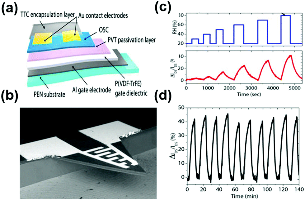 | ||
| Fig. 22 (a) Schematic representation and (b) SEM image of an OFET-integrated MEMS sensor device; (c) (above) relative humidity introduced and (below) corresponding current response of the device; (d) repeatable behavior of the device in an 80% RH environment (reprinted with permission from Thuau et al.,174 copyright 2016, Nature). | ||
2.2 Semiconducting materials for light sensing (phototransistors)
The preparation of flexible phototransistors for wearable electronics (e.g., in healthcare and environment monitoring systems) requires the use of semiconducting materials that simultaneously show a degree of mechanical flexibility,29 nontoxicity, and biodegradability.175,176 Indigo and its brominated derivative (6,6′-dibromoindigo (6-BrIG)) can be considered classic examples of safe and nontoxic organic semiconducting materials.175,177 Indigo and 6-BrIG were known to be the subjects of the world's oldest chemical industry, being manufactured from natural sources and valued as much as gold.178–180 Among these, 6-BrIG is of particular interest since it demonstrates the optoelectronic properties desired for the successful functionality of a phototransistor.175,181–183 6-BrIG exhibits strong inter- and intramolecular hydrogen bonding between its carbonyl and amine groups, which decreases the π–π stacking distances and induces planarity, both of which are favorable for effective charge transport. Air-stable electron transport is promoted by its low-lying LUMO level (3.7 eV), whereas the ambipolar charge injection is enabled by the small bandgap (1.8 eV). The addition of a broad absorption band (350–700 nm) of 6-BrIG implies facile electronic excitation upon exposure to visible light. Hence, 6-BrIG can be considered an attractive candidate to be used as a photoactive material. For instance, Kim et al. have recently reported on the fabrication and characterization of 6-BrIG-based ambipolar OPTs, having n-channel photoresponsivity and external quantum efficiency of 10.3 A W−1 and 2437%, respectively, and p-channel photoresponsivity and external quantum efficiency of 0.0554 A W−1 and 13.1%, respectively.183In the OSC family, π-conjugated polymers show improved solution-processability, and better compatibility with flexible substrates. Furthermore, from a molecular viewpoint, polymers exhibit broader optical absorption, and much larger conjugation lengths which renders them more valuable for optoelectronic devices,44 compared to small molecules.184,185 For application in OPTs, polymers are essentially required to demonstrate wide absorption and high μFET, such that the process of effective light absorption, exciton dissociation and charge transport is facilitated.44,186 Kim et al. used the photoactive polymer, poly[2,5-bis(2-octyldodecyl)pyrrolo[3,4-c]pyrrole-1,4(2H,5H)-dione-(E)-1,2-di(2,20-bithiophen-5-yl)ethene] (PDPP-DBTE), to fabricate OPTs in a TGBC architecture with PMMA as the gate dielectric (Fig. 23a).187 Under illumination intensities of 3, 5, 9 and 15 mW cm−2, the OPTs showed a substantial increase in ID and shift of VT to positive values (Fig. 23b). In principle, following the photogeneration of charge carriers in the PDPP-DBTE layer, holes flow to the drain electrode whereas electrons mostly accumulate under the source electrode (Fig. 23c). The latter phenomenon can cause lowering of the hole injection barrier, leading to a positive shift in VT. Overall, owing to the favorable optical properties of PDPP-DBTE, the OPTs developed by Kim et al. showed promising results with a photo-to-dark current ratio exceeding 5 orders. In addition, the devices showed an on-state photoresponsivity of ∼2.5 A W−1, and off-state photosensitivity of ∼1.54 × 10⁵ (Fig. 23d).
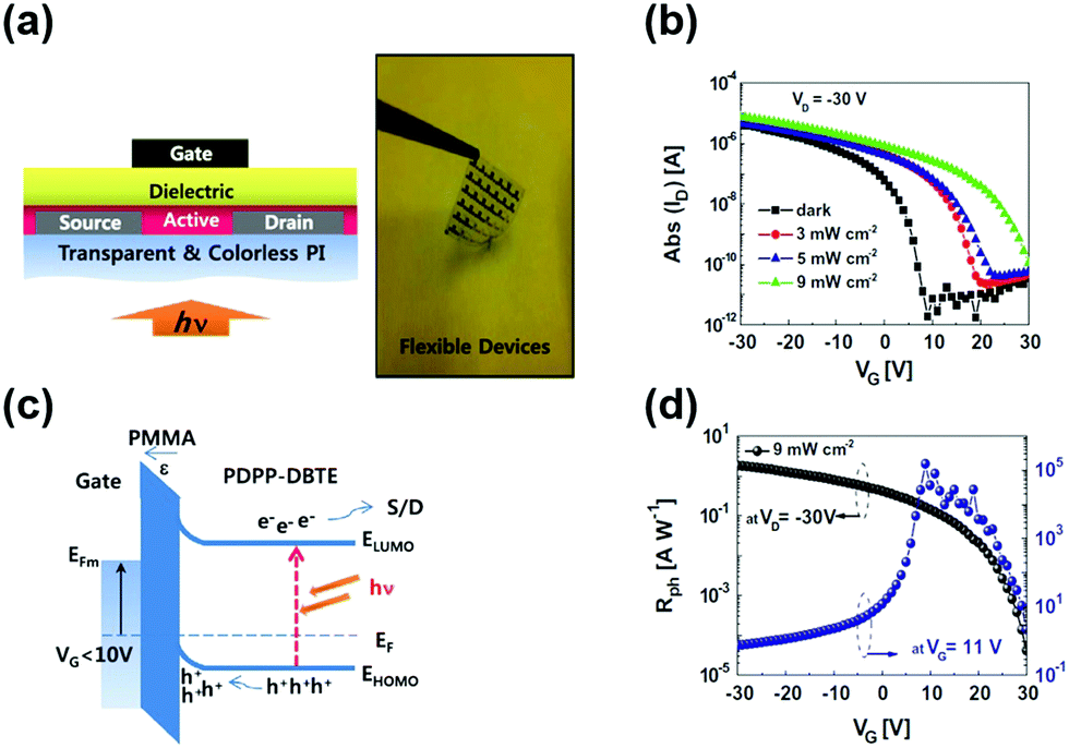 | ||
| Fig. 23 (a) Schematic illustration of PDPP-DBTE-based OPTs and photograph of devices fabricated on flexible substrates; (b) ID × VGS characteristics in the dark and under illumination at various light intensities; (c) energy band diagram of PDPP-DBTE-based OPTs under illumination conditions with a negative VGS; and (d) photoresponsivity and sensitivity as a function of VGS (reprinted with permission from Kim et al.,187 copyright 2014, Elsevier). | ||
Pentacene is a desirable choice as far as wearable electronic applications are concerned since it is nontoxic, biocompatible, biodegradable, and mechanically flexible.188,189 Thin films of this small molecule formed via evaporation consist of a highly ordered molecular structure in a “herringbone” arrangement.190,191 The solid-state structure is dominated by strong intermolecular interactions, which promotes a high degree of crystallinity and efficient charge transport properties.192 Pentacene is typically known to yield μFET values of ∼1 cm2 V−1 s−1 in OFETs,120,193 while the devices in which single crystals of pentacene are utilized are reported to show a μFET of ∼60 cm2 V−1 s−1.194 In the case of phototransistor applications, pentacene is widely utilized in the research industry because of its small bandgap (2 eV) and relatively broad absorption band (300–600 nm). In SiO2/pentacene-type devices, Debucquoy et al. have attributed the phototransistor effect to the trapping of photogenerated electrons by OH groups at the I/S interface.195 Moreover, in a recent work, Park et al. have combined the nontoxic OSC (pentacene) with the biodegradable and flexible substrate (cellulose nanofibrillated fiber) to prepare high-performance phototransistors.196 The devices withstood over 2000 bending cycles, and the use of environmentally friendly materials resulted in exceptional biodegradability characteristics, as confirmed by the fungal biodegradation test. Similarly, it was reported that the use of highly transparent nonmetallic electrodes (molybdenum trioxide-buffered indium zinc oxide) lead to phototransistor transmittance over 70%. This study not only further asserts the potential of pentacene-based phototransistors in wearable electronics but also highlights the advantage of combining biodegradable substrates for the realization of eco-friendly disposable systems.
Recent studies have highlighted DA copolymers as promising materials for OPT applications because of their low bandgap, which facilitates the harvesting of incident photons for effective charge carrier generation.197–200 Wang et al. used a PBTIDBIBDF copolymer, blended with poly(1,4-butylene adipate) (PBA), to fabricate low-voltage and flexible OPTs (Fig. 24a).201 The devices showed P and R values of 5.7 × 10⁴ and 180 mA W−1, respectively, while an increase in the illumination intensity was observed to induce a higher ID and larger VT shifts (Fig. 24b). Furthermore, the devices showed fairly stable photocurrent behavior under various on/off illumination cycles. The efficient photoresponse of these OPTs was attributed to the utilization of the PBTIDBIBDF copolymer as the photoactive layer, which exhibits highly ordered molecular packing, assisting in the effective transport of separated charge carriers under illumination. Similarly, the polar groups in the PBA molecules induced the charge trapping effects at the I/S interface, which improved the photosensitivity by causing significant shifts in VT (Fig. 24b). The photoresponse behavior of PBTIDBIBDF-based OPTs can be further understood by the energy band diagram in Fig. 24c. The application of VGS results in the accumulation of holes (that form positive donor areas) at the I/S interface. When the device is illuminated, free electrons and holes are generated in the PBTIDBIBDF layer, and the recombination of electrons and holes causes a positive shift in VT. The increase in illumination intensities causes an increase in the recombination ratio, thereby resulting in a larger VT shift. This also reveals that the PBTIDBIBDF-based OPTs operated in the photovoltaic mode.
 | ||
| Fig. 24 (a) Flexible PBTIDBIBDF-based OPTs fabricated in the BGTC architecture; (b) ID × VGS characteristics of OPTs under various illumination intensities (VDS = −5 V); and (c) schematic illustration of the OPTs and energy band diagrams elucidating the photoresponse behavior (reprinted with permission from Wang et al.,201 copyright 2019, Wiley-VCH). | ||
2.3 Semiconducting materials for pH sensing
A pH sensor plays an important role in maintaining quality control in laboratory experimentation within a wide range of scientific areas, including bioelectronics,202–204 agriculture,205 oil,206 water quality,207 and drug delivery industries.208 Although researchers around the world have been developing state-of-the-art pH sensors, there is still difficulty in making them cheap and easy to use. A good example is the paper-based colorimetric sensor, which is both low in cost and easy to make and use.209 However, some cases require more stable devices where the temperature exceeds the room ambience. In this context, OFET has proved to be a promising candidate since it can be operated at low voltages and provides enhanced sensitivities in various sensing conditions.210–212 It is important to note that bottom-gate OFET geometries are commonly preferred to avoid any kind of damage induced by the gate dielectric on the surface of the OSC.133,213 One of the important drawbacks in this architecture, however, is the direct contact of the organic materials with the ambient conditions. To overcome these issues, Diallo et al. reported on a top-gated OFET-based ion-sensitive pH sensor prepared on Kapton flexible substrates using pentacene as the OSC.214 This sensor consists of chemically inert parylene as the gate dielectric material, deposited on the surface of a pentacene active layer. The schematic representation of the as-fabricated device is shown in Fig. 25a.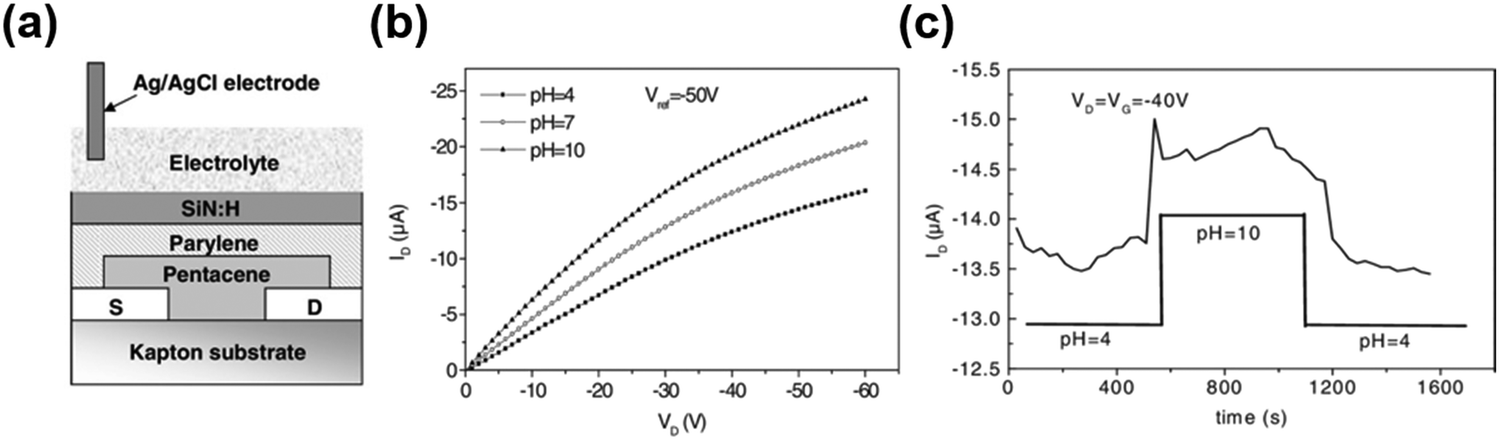 | ||
| Fig. 25 (a) Schematic representation of flexible OFET device, (b) output characteristics and (c) transient response of device toward pH = 4, 7, and 10 (reprinted with permission from Diallo et al.,214 copyright 2008, American Institute of Physics). | ||
In the initial stage of investigation, an increase in ID was observed when the pH level was increased from 4 to 10 (Fig. 25b). In addition, the reported device showed good response and recovery behaviors (Fig. 25c), attributed to the use of the parlyene dielectric and due to the slow annealing process of SiN:H.214 Although the devices demonstrated good sensitivity to a wide pH range, the successful device operation relied on the use of a reference electrode (Ag/AgCl in Fig. 25a), which can be considered a barrier for integrating such devices in wearable and disposable applications. To overcome this issue, unique counter-electrodeless or freestanding ion-sensitive FET (ISFET) architecture was proposed by Caboni et al.215 The proposed architecture consisted of two independent devices: a capacitor (Fig. 26a) and a pentacene-based OFET (Fig. 26b).
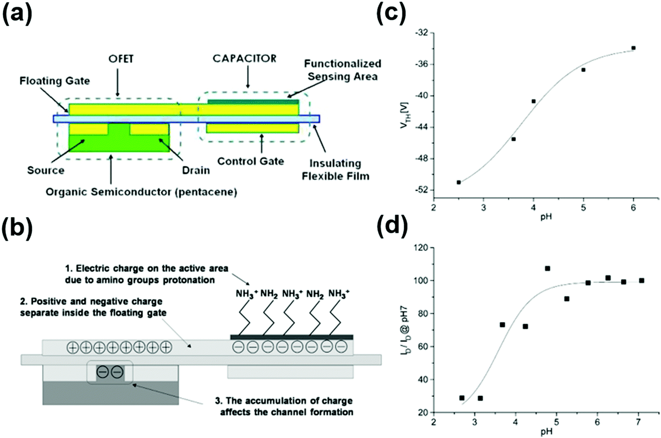 | ||
| Fig. 26 (a) Schematic representation and (b) pH-sensing mechanism of a flexible OFET device; (c) threshold voltage behavior and (d) sensitivity of the device toward different pH conditions (reprinted with permission from Caboni et al.,215 copyright 2009, IEEE). | ||
In this intricate device architecture, the capacitor and OFET devices are connected by the floating gate. The device mechanism is dominated by the electric field applied at the control gate and common source terminals, respectively. The electric field applied at the control gate terminal influences the biasing condition of the adjacent OFET via the floating gate terminal. The device operation mechanism takes the effect of pH sensing, which manifests itself by a change in ID of the OFET device. One of the most crucial parts of this device is the effective functionalization of the floating gate surface with thio-aminic groups, which helps in determining the pH of the solution. When the test solution is exposed to the modified floating gate, a desired protonation and deprotonation cycle takes place based on the pH of the solution. Such chemical cycles change the charge density of either holes or electrons in the floating gate terminal. This, in turn, modifies the charge carrier concentration in the semiconducting channel of the adjacent OFET device. This process can be well understood with the help of the pH-sensing mechanism shown in Fig. 26b. The results obtained by Cobini et al. while using the ISFET sensor architecture are shown in Fig. 26c and d. The device showed good sensitivity behavior between pH levels 3 and 5, which is evident by the significant variation of both ID and VT of the OFET.
Although the authors successfully demonstrated a highly sensitive and reproducible pH-sensing device,215 the high operating voltage makes it inappropriate for wearable device applications. This issue has been recently addressed by Li et al., who developed a low-voltage, highly sensitive, and flexible pH sensor platform using the ISFET architecture.216 Different from the architecture proposed by Caboni et al.,215 the device architecture of Li et al. consisted of three key components: the OFET device, the working electrode, and the reference electrode.216
The OFET devices were fabricated on a PEN substrate. Firstly, the bottom gate and top source/drain contacts were formed by inkjet printing of silver ink. Subsequently, both the buffer layer and the gate insulator thin film were deposited by spin coating the PMMA solution on the gate, while the active channel was formed by drop casting the TIPS-pentacene:PS blend solution on top of the source/drain contacts. The as-fabricated OFET device was then separated from the original PEN substrate and transferred to a common PET substrate. Similarly, the other two important components of the sensing device, the reference electrode (Ag/AgCl/PVB) and the working electrode (ITO), were also formed on top of the PET substrate. Hence, all three major components of the device were integrated on a common PET platform, as shown in Fig. 27a.
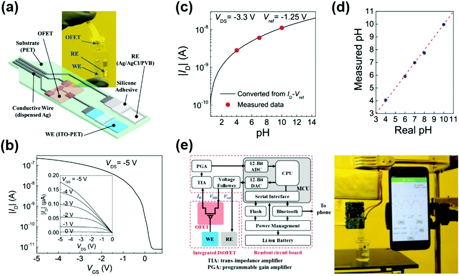 | ||
| Fig. 27 (a) Schematic representation and (b) transfer with (inset) output behavior of an ion-sensitivity OFET (IOSFET) device; (c) relation between measured drain current and pH condition; (d) comparing the measured and standard pH values; (e) pH value reading circuit and real-time pH measuring set up using an as-fabricated flexible IOSFET device (reprinted with permission from Li et al.,216 copyright 2018, IEEE). | ||
As presented in Fig. 27b, the as-fabricated TIPS-pentacene:PS-based OFET device operated at low voltages and showed a promising Ion/Ioff of around 105. Subsequently, the open-circuit potential difference was measured between the working and reference electrodes under different pH conditions. Notably, the pH was observed to maintain a linear relationship with respect to the measured voltage over a long period. To present a real-time model, a concrete relationship between the pH of the solution and the output current of the OFET device is required. To obtain this, an experiment was conducted in which the pH of the testing buffer solution was varied and the corresponding changes in ID were observed (Fig. 27c). For fixed reference and drain voltages, ID was observed to change nonlinearly for pH ranging from 2 to 14. In addition, the measured data also satisfied the theoretical values (Fig. 27d). Based on the obtained results, the electrical data readout circuits were developed and interfaced with the as-fabricated ISFET, as shown in Fig. 27e. In conclusion, Li et al. successfully demonstrated the pH-sensing behavior and, at the same time, wireless transmission of data to a mobile phone to visually observe the change in pH values of a given solution with respect to time (Fig. 27e). Hence, the reported device shows great potential to satisfy the requirements for future IoT-based smart-sensing applications.
2.4 Semiconducting materials for early disease diagnosis
Disease diagnosis is another important sector that constantly requires innovation and huge production capability.217–221 As most of the diagnostic elements are not reusable and require regular replacement, it is favorable to adopt disposable elements with low cost.222–224 Reactive oxygen species (ROS) are important signaling agents for diagnosing diseases at an early stage in human beings.225–227 During a disease period, some of the cells’ metabolic activities and their associated functions tend to generate biomolecules such as superoxides, which come under the class of ROS.227 Jeong et al. have proposed a novel combination of rutin, a type of polyphenol, and conjugated polymer for the detection of superoxides secreted by the mouse macrophages.228 The proposed sensing device, with the BGBC configuration, was fabricated by initially patterning the flexible PET substrate with ITO, which acted as the bottom-gate electrode (Fig. 28a). Subsequently, the spin-coating method was employed for depositing the gate dielectric (PMMA) on the surface of the as-prepared flexible substrate on top of which the source and drain electrodes were lithographically patterned. The active sensing layer (rutin-P3HT hybrid) was spin coated on the surface of the source/drain electrodes. In the first stage of investigation, after careful optimization, the proposed device showed good transistor performance when the rutin content was around 10 wt% in the host polymer material. However, the threshold voltage of the p-type rutin-modified device exhibited more positive voltage along with an increase in off current. Here, this problem may be mitigated by exploring more on the interface engineering with solvents other than toluene. As it is not an orthogonal solvent, it could have generated traps at the P3HT and PMMA, leading to increased roughness at the I/S interface regions.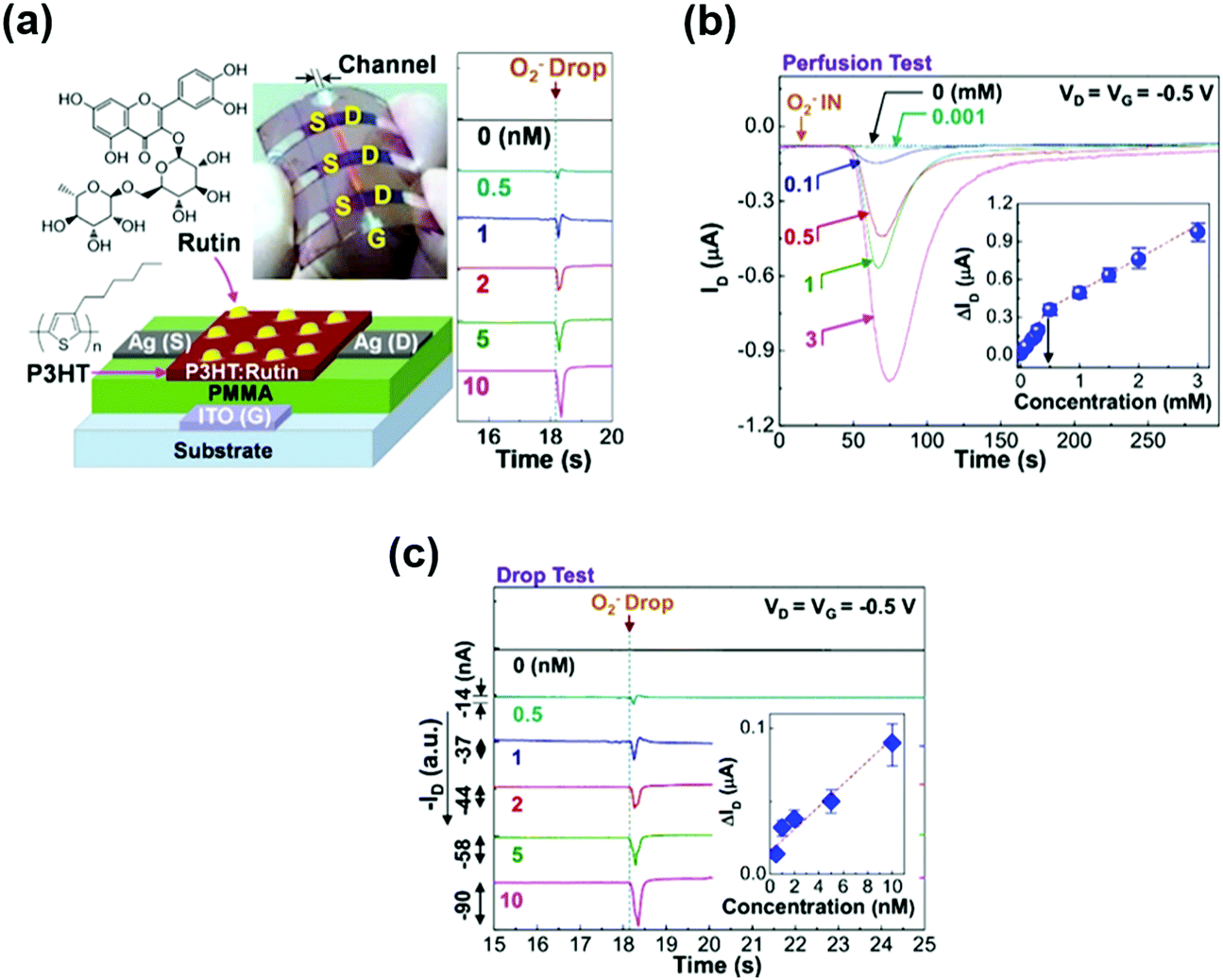 | ||
| Fig. 28 (a) Schematic illustration of a P3HT:rutin-based flexible OFET device, (b) perfusion, and (c) drop test of the OFET device toward different lactate concentrations (reprinted with permission from Jeong et al.,228 copyright 2018, Elsevier B.V.). | ||
The superoxide-sensing studies of the proposed OFET device were performed at 0.5 mM O2− molecules in the buffer solution. In this case, the OFET responded with a time lag of ∼50 s. As a result, irrespective of the increase in applied gate and drain voltages, an increase in relative drain current sensitivity with respect to time was observed. To find the LOD of the proposed device for the target superoxide, two methods were employed: the perfusion method and drop test. In the former, under constant gate and drain voltages of −0.5 V each, the concentration of the O2− superoxide molecules was tuned from 0 to 3 mM. As shown in Fig. 28b, the proposed device was observed to sense as low as 0.001 mM O2− concentration. Here, hydroxyl groups in rutin molecules interact with superoxide species in aqueous solutions and form H2O2 and oxygen anions. Thus, the positive charge gets doped in P3HT with these oxygen anions, increasing the response current. Unlike the perfusion technique, the drop test method played a vital role in observing the sensitivity of the proposed OFET sensing device down to an nM O2− concentration range. In this case, the device under testing showed ultrahigh sensitivity by successfully detecting 500 pM O2− ions concentration, which implies a difference of four orders of magnitude compared to the perfusion method, which can be seen in Fig. 28c. This can be explained as a result of the availability of abundant binding sites for the interaction to take place. In the former case, the presence of inlet and outlet in the flow cell could have led to less interaction time, thereby leading to a minimal LOD. However, in the case of the drop test, the entire solution is concentrated around the device with improved interaction time. As a result, the available O2− gets enough time to interact with target analytes since no flushing is involved.
In addition to sensing studies, based on the requirements of real-time applications, the authors also conducted operational stability and device reusability tests. Interestingly, the reported device successfully responded to various superoxide concentrations, ranging from 0.1 mM to 3 mM, repeated ten times. Moreover, by using a PBS buffer solution, the as-fabricated sensor exhibited satisfactory superoxide response after 15 days of cold storage. In summary, the study by Jeong et al. reported a sensor that is mechanically flexible and highly sensitive, showing stable and reliable detection of superoxide molecules from living organisms.228
2.5 Semiconducting materials for drug abuse detection
In the modern era, drug-based tablets are commonly prescribed medications for various diseases. Among many, amphetamine-type stimulants (ATS) are one of the most popularly prescribed drugs for treating health problems such as asthma, diabetes, and so forth.229–232 However, this easy access to such strong prescribed medications can very easily lead to drug abuse and addiction. According to the WHO, in recent years, young people from different parts of the world have been reported to illegally consume ATS drugs for boosting their physical and mental activities.233 At present, the widely used systems for detecting ATS analytes are based on chromatography,234 spectroscopy,235 and molecularly imprinted polymers.236,237 However, these systems are bulky and costly, which obviously stands as a barrier for large-scale usage. A viable solution was recently proposed by Jang et al., who reported on a low-cost, highly sensitive, and wearable OFET-based ATS sensing system.238 The BGTC DDFTTF-based OFETs were fabricated on Si/SiO2 substrates (Fig. 29a), and the receptor–analyte interaction strategy was used for selectively sensing ATS biomolecules from various aqueous solutions. Hence, the cucurbit[7]uril (CB[7])-based derivatives were spin coated on the surface of the OSC. Based on the results from NMR and XRD analysis, the CB[7] receptor molecules tend to show weak van der Waals force of interaction with the target ATS biomolecules. Here, the authors used CB[7] derivatives since they are soluble only in water, whereas the OSC (DDFTTF) is immune to water. Thus, they adopted an orthogonal solvent technique to deposit a bilayer stack of both channel layer and receptor layer. This approach apparently improved the easy thin-film formation of CB[7] on top of DDFTTF without degrading the channel characteristics. The electrical characteristics of the OFET device with and without CB[7] were initially measured. As shown in Fig. 29b, the former device architecture exhibited the transfer characteristics with high hysteresis when compared to their non-CB[7] counterpart. However, both the device architectures notably presented a Ion/Ioff ratio of around 105. Subsequently, the ATS-sensing properties of the CB[7]-modified DDFTTF-based OFET device were investigated. The as-fabricated device was primarily exposed to different concentrations of ATS with distilled water as a base reference solution. As a result, in the case of one of the CB[7] derivatives, allyloxyCB[7], the modified OFET device showed good sensitivity for ATS concentration as low as 1 pM. Unlike an allyloxyC[7] derivative, its phenylbutoxyCB[7] counterpart exhibited good sensitivity toward a wide range of ATS concentrations from 1 pM to 1 μM, having standard PBS as the base solution. Furthermore, to mimic real-time testing conditions, the phenylbutoxyCB[7] functionalized OFET device was used for sensing ATS molecules in biological urine samples. Interestingly, the device under testing presented excellent sensitivity toward a narrow range of ATS concentrations from 0.1 nM to 10 nM, as shown in Fig. 29c. | ||
| Fig. 29 (a) Schematic illustration and (b) transfer characteristics of a DDFTTF OFET on a silicon substrate, (c) OFET device response toward different concentrations of ATS analytes in urine samples, (d) schematic representation of the DDFTTF-based flexible OFET device, (e) photograph demonstrating the integration of the flexible OFET device on the wristband for real-time monitoring application (reprinted with permission from Jang et al.,238 copyright 2017, Elsevier Inc.). | ||
In the next stage of investigation, for achieving low-voltage operation conditions, the reported sensors were fabricated on ITO/PEN flexible substrates, having Al2O3 as the gate dielectric and CB[7]-functionalized DDFTTF as the active channel material (Fig. 29d). When the as-fabricated flexible device was exposed to 1 pM ATS molecules with distilled water as the base solution, a good sensing response was observed at operating voltages of −1.5 V (VDS) and −10 V (VGS), which is much lower than those of the Si/SiO2 devices. As shown in Fig. 29e, Jang et al. successfully demonstrated the real-time usage of the proposed ATS sensor. In essence, a low-power, cost-effective, and portable ATS sensor for biomedical applications was developed that shows high sensitivity and selectivity toward target analytes.
2.6 Semiconducting materials for other sensing target applications
As seen in Fig. 30a, the OFET devices were fabricated on flexible PET substrates, having parylene-C as the gate dielectric material. Two OSCs (pentacene and P3HT) were employed, and their strain-sensing properties were tested. The pentacene-based strain sensor displayed good sensitivity and a linear response over a short range of strain when compared to the P3HT device (Fig. 30b). This behavior was attributed to the large grain sizes, and uniform thin film formation was confirmed with the help of AFM images. Based on these results, the as-fabricated sensor was tested under real-time conditions. In the beginning, the sensor was subjected to intensive bending conditions for different angles ranging between 90° and 180°. Interestingly, the as-fabricated strain-sensing system differentiated each bending angle with the equivalent drain current (Fig. 30c), and the reported device remained both mechanically and electrically stable even after 100 bending cycles (Fig. 30d). These outcomes clearly highlight the robustness and reliability of employing these devices in flexible strain-sensing applications.
 | ||
| Fig. 30 (a) Schematic representation of a P3HT based OFET flexible device. (b) Comparison of P3HT and pentacene device current response for different pressure and strain conditions applied. (c) Distinct current response for a wide range of device bending conditions from 180 to 90 degree. (d) Repeatable (100 times) current response of the device under 90 degree bending radius strain condition (reprinted with permission from Loi et al.,246 copyright 2013, IEEE). | ||
Along with this report, many research groups have strongly suggested that under applied strain, the change in electrical behavior is mainly due to the structural deformation of the active OSC material.248–250 However, Scenev et al. have detected that a detailed study regarding the relationship between applied strains and their relative changes on the structural properties of OSC was lacking.239 Thus, to understand this relationship, Scenev et al. investigated the electromechanical properties of pentacene-based flexible OFET devices for strain-sensing-based applications. The OFET devices were fabricated on flexible PET substrates and utilized PVA as the gate dielectric (Fig. 31a). In this case, a special bending apparatus was employed to produce uniform strain conditions over the whole device area. The transfer characteristics of the as-fabricated flexible device were measured under two different conditions. Primary test results show that the device displayed hysteresis-free electrical characteristics for an applied strain of less than 2%. From the latter test, the hysteresis drastically increased with the strain applied from 0 to 3.3%, as shown in Fig. 31b. To understand this behavior, both scanning force microscopy (SFM) and XRD characterization on a PEN-modified PVA dielectric was performed. When the PEN layer was deformed from 0 to 1.3%, the SFM results confirmed that there is no significant shift in the inter-grain boundary distance (Fig. 31c). In contrast, the inter-grain boundary distance gradually increased when the applied strain reached 10% (Fig. 31d). Moreover, the XRD results confirmed that there is no deformation in the PEN crystal structure for the applied strain of about 10%. Hence, with the help of these results, Scenev et al. have suggested that upon the application of strain, the potential barrier for the electron flow between the grain boundaries tends to increase. This, in turn, decreased the μFET and ID along the channel at the I/S interface region, which satisfied the results observed in Fig. 31b. Notably, the gold electrodes, on top of the OSC, lost their mechanical stability for the strain <2%. This stands as a barrier for using the proposed device as a reliable strain sensor. To overcome this problem, Scenev et al. suggested the use of soft yet highly conductive electrodes for improving the sensitivity and lifetime of the proposed flexible OFET-based strain sensor.
 | ||
| Fig. 31 (a) The fabricated pentacene OFET device stack. (b) Transfer characteristics of device for different strain conditions from 0 to 3.3%. AFM height images recorded after applying (c) 1.3% and (d) 10% strain on pentacene film (reprinted with permission from Scenev et al.,239 copyright 2013, Elsevier B.V.). | ||
Another approach for improving the sensitivity toward applied strain is the integration of micro-electromechanical systems (MEMS) technology in the OFET device architecture. It is important to note that the growth of inorganic MEMS-based sensors has drastically declined in the past decade due to their poor compatibility in flexible and wearable applications.251 Alternatively, the organic MEMS device concept is growing rapidly because of the intrinsic high sensitivity to mechanical deformations.174 For developing sensitive strain sensors, the mechanism that bridges the gap between MEMS and OFET is the mechanical-to-electrical conversion technique.172 In this context, Damien et al. combined the versatile properties of a MEMS-based organic cantilever with OFET devices using a piezoelectric mechanism for strain-sensor application.174 Owing to the air stability requirement, pentacene and DNTT organic small molecules were chosen for fabricating the OFET-embedded cantilever device architecture. Here, the piezoelectric P(VDF-TrFE)/PVT polymer was employed as the gate dielectric material. As shown in Fig. 32a, the electrical characteristics of the as-fabricated OFET device were studied with different poling conditions which is crucial for understanding their strain sensing capabilities.
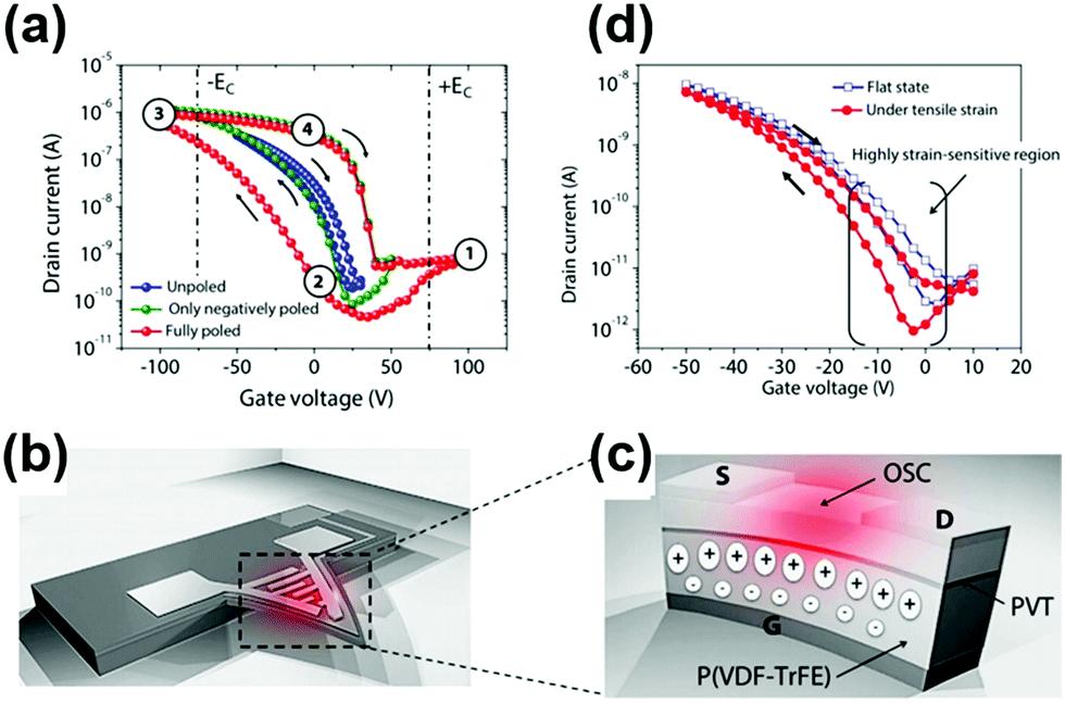 | ||
| Fig. 32 (a) Comparison of transfer characteristics and associated hysteresis behavior for different poling conditions. (b) Effect of strain and (c) corresponding impact on the dipole properties of the P(VDF-TrFE) layer. (d) Change in device transfer characteristics under applied tensile strain conditions (reprinted with permission from Thuau et al.,174 copyright 2016, Nature). | ||
It is clear from the figure that the hysteresis in the drain current response was enhanced with the level of sweeping voltage. This result is attributed to the influence of polarization parameters in the piezoelectric gate dielectric by the applied gate bias. The schematic representation of the strain-induced changes in the device are presented in Fig. 32b and c. When the cantilever tip is subjected to mechanical strain, shifts in both drain current and threshold voltage are witnessed (Fig. 32d). This is due to a positive polarization effect induced in the gate dielectric material. This, in turn, influenced the charge density in the channel region of the OFET device. As a result, the sensitivity of the pentacene-based OFET-cantilever hybrid device was measured to be around 600, which is around five times greater than the DNTT-based strain sensor. This report also highlighted the importance of the polarization effect in the piezoelectric gate dielectric material for augmenting the sensitivity toward the change in strain levels. The above discussed literature reports have critically failed to project the real time capability of the sensor. Demonstrating the real time potential of the homemade sensor is crucial to bridge the gap between the laboratory inventions and the practical devices. In light of this requirement, Lai et al.252 have not only fabricated a novel and low power flexible strain sensor but also successfully integrated it into commercially available gloves to monitor hand movement. This embedded sensor was connected to the custom-designed readout circuits to convert the current into useful voltage levels which can then be processed for conveying required information to the people. Even-though the authors have demonstrated the effective use of strain sensors in transducing the hand movement, they ended up with a bulky system. Hence, still there is a need to develop a smart, compact, flexible, low power and high performance flexible strain OFET sensor system to satisfy the demand of wearable electronics.
Song et al. have recently proposed a novel combination of polymer-dispersed liquid crystal (PDLC) and an OFET device for realizing a multi-sensing platform.240 The BGBC P3HT-based OFET devices were fabricated on PEN flexible substrates with PMMA/P(VDF-TrFE-CFE) as the bilayer gate dielectric (Fig. 33a). This device was then considered for testing its sensing capability toward different external stimulants such as heat, light, airflow, and physical touch. When the device was subjected to N2 gas flow, ID increased linearly with the gas flow ranging between 0.1 and 10 sccm. With an increase in gas flow, a small amount of pressure was experienced by the surface of the PDLC layer, which resulted in drifting the negative dipoles of the 4,4′-pentyl-cyanobiphenyl (5CB) microdots downward. This increased the hole-charge carrier density and, thus, the drain current in the OFET channel region.
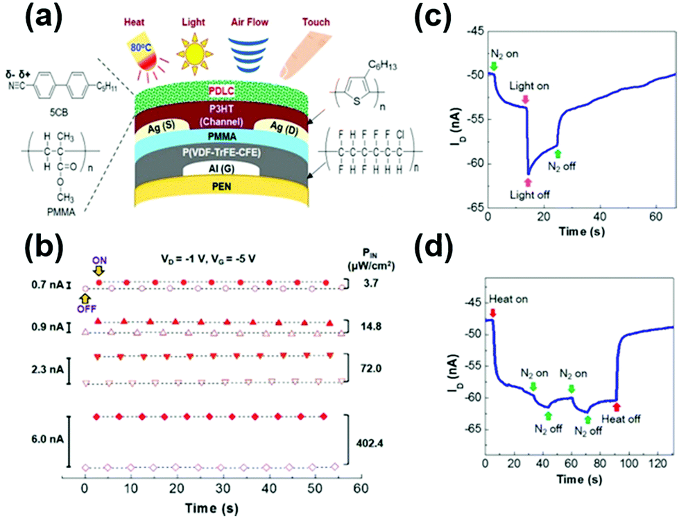 | ||
| Fig. 33 (a) Schematic representation and (b) photo-response of the bottom contact OFET device with a dual polymer gate dielectric. Multi-sensing device response toward (c) N2 and light, (d) heat and N2 stimulants (reprinted with permission from Song et al.,240 copyright 2017, Nature). | ||
A similar sensing mechanism was proposed when the as-fabricated device was subjected to the applied load. As a result, when compared to the N2 flow response, the change in drain current steeply increased with the load applied between 0.1 and 10 g. It is worth noting that in both N2 flow and load-sensing cases, the electrical dipole moment of the PDLC layer influences the charge-carrier transport behavior in the P3HT layer. Interestingly, as shown in Fig. 33b, when the incident light (550 nm) power increased from 3.7 to 400 μW cm−2, the drain current increased from 0.7 to 6.0 nA. This behavior was observed because when light is absorbed by the P3HT layer, exciton pairs are generated, which increases the dominant charge-carrier concentration along the channel. Subsequently, the temperature-sensing capability of the proposed PDLC-based OFET device was observed. At drain and gate voltages of −1 V and −5 V, respectively, the relative current sensitivity gradually increased with temperatures from 40 to 70 °C. This increased drain current is due to the effect of thermally induced hole-carrier mobility along the P3HT/PDLC interface.
Recently, our group261 has successfully developed a fully flexible, biocompatible, and wearable device with good stretchable nature. This homemade skin platform was successfully integrated with a biocompatible sensor. The combination of the proposed magnetic skin and the associated sensor was demonstrated by installing them in the vicinity of the eye to monitor the movement of eyelids. As a next step to this research work, we can integrate the developed system with the circuit system (comprising an amplification block and Analog to Digital circuit (ADC)) that can be completely realized using organic transistors.261
In the next step of investigation, the multi-sensing capability of the proposed device was reported. Primarily, the device was simultaneously exposed to N2 flow and light. As seen in Fig. 33c, the drain current increased gradually and then sharply decreased when exposed to N2 flow and light exposure, respectively. After turning off the light and gas flow, the device retreated back to the base current. Similar experiments were conducted to test the as-fabricated device with the combination of heat and nitrogen gas. From Fig. 33d, it is clear that the current change with respect to the applied heat is more significant than the effect of nitrogen gas. In conclusion, low-cost, flexible, and compact PDLC-based P3HT OFET devices exhibited excellent multi-sensing capability toward various external stimulant conditions.
An optically transparent and mechanically flexible sensor with multi-sensing capability is in high demand for satisfying the requirements of robotic applications.241 However, some of the bottlenecks in realizing such a sensor include the choice of materials and employing low-temperature processing techniques, which can assist in fabricating simple yet innovative devices on low thermally stable flexible substrates.262–264 Trung et al. studied the mechanical and temperature-sensing capabilities of the pentacene-based OFET devices fabricated on flexible PES substrates (Fig. 34a).241 Here, the multi-sensing capability of the proposed devices was mainly attributed to the crystalline nature, as well as pyroelectric and piezoelectric properties, of the gate dielectric P(VDF-TrFe). In addition to the dominant electric dipole properties of the gate dielectric, the properties of the OSC and the substrate may also influence the sensing response. To avoid these negative effects, an AC gate bias was applied to measure the dielectric potential or voltage (V0). This measured voltage precisely changes with respect to the applied multiple stimulant conditions. To observe this effect, the as-fabricated device was primarily exposed to different physical stimulants, such as IR illumination, pressure, and strain excitation individually, and the corresponding changes in V0 values were measured. With the increase in incident IR power from 0 to 2000 mW cm−2, the gate-dielectric crystal layer experienced thermal expansion due to a positive pyroelectric effect. This leads to the increase in electric dipole moment, which results in a linear increase of V0, as seen in Fig. 34b.
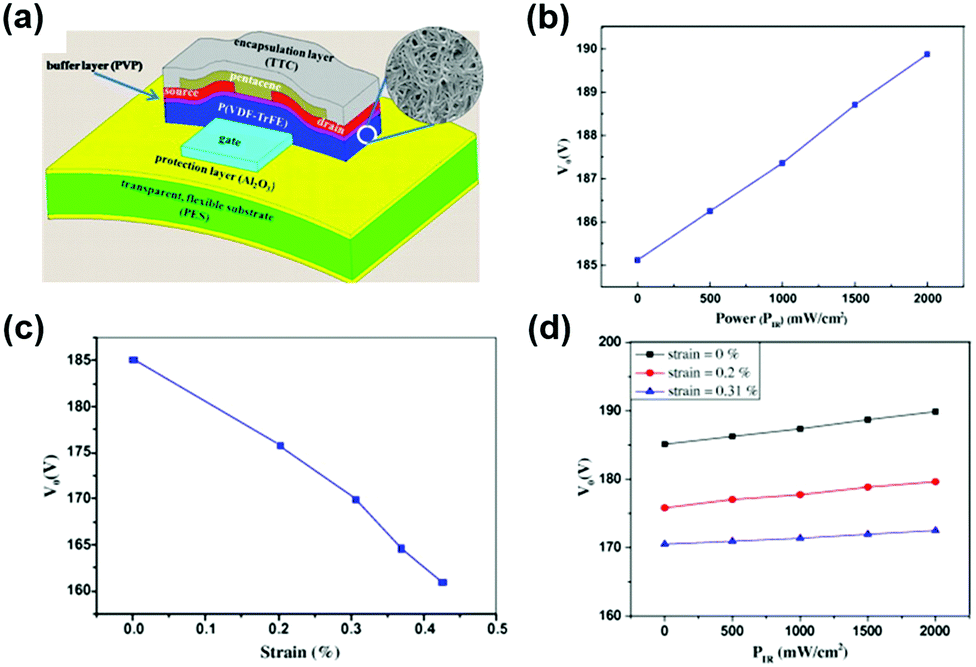 | ||
| Fig. 34 (a) Illustration of materials used in bottom gate bottom contact pentacene OFET flexible device. Device voltage response toward (b) incident light, (c) applied strain and (d) combination of both light and strain (reprinted with permission from Trung et al.,241 copyright 2012, Elsevier B.V.). | ||
In contrast, when the mechanical deformations such as pressure and strain were applied, due to a negative piezoelectric effect, V0 showed a reduction (Fig. 34c). Subsequently, the multi-sensing capability was tested by simultaneously exposing the as-fabricated device to IR radiation and strain. Fig. 34d shows the plot of V0 as a function of IR radiation power for different strain conditions. With the increase in IR radiation and strain, V0 increases due to a positive pyroelectric effect, and the voltage level shifts down because of the piezoelectric mechanism. Furthermore, the authors also tested the effect of mechanical deformation on the sensing performance of the proposed device. Even after 104 bending cycles, irrespective of external stimulants, the degradation of the device's sensing capability tends to reduce with the increase in bending radius from 1 cm to 1.5 cm of the proposed flexible device. Such characteristics validate the development of a mechanically flexible, portable, cost-effective, and multifunctional OFET device. In summary, the sensing performances of the recently reported flexible OFET based strain and multimodal sensors are presented in Table 4.
| Material | Sensor application | Sensitivity | Device | Limit of detection | Media | Flexibility limit |
|---|---|---|---|---|---|---|
| a PEN = polyethylene naphthalene, PES: polyestersulfone, PDLC: polymer dispersed liquid-crystal. | ||||||
| 10 | Strain sensor239 | 15% | BGBC OFET | 0.01 N | Kapton | No information |
| 8 | Strain sensor174 | 600 | Cantilever OFET | <0.3% | PENa | No information |
| 10 + PDLCa | Multimodal sensor240 | Gas flow: 2 nA sccm−1 | BGBC OFET | 0.2 sccm | PENa | No information |
| Pressure: 1 nA g−1 | 0.8 g | |||||
| Light: 0.2 nA (μW cm−2)−1 | 3.7 μW cm−2 | |||||
| Temperature: 0.06 nA °C−1 | 40 °C | |||||
| 8 | Multimodal sensor241 | Light: 3 mV (mW cm−2)−1 | BGBC OFET | 0.1 mW cm−2 | PESa | Bending radius: 1.5 cm |
| Pressure: 10 V MPa−1 | 0.15 MPa | |||||
| Strain: 50 V per % | 0.1% | |||||
3. Outlook and conclusion
Mechanical flexibility of electronic devices can be considered an important criterion due to the ever-growing need for making electronics conformable around objects, which will eventually lead to the development of wearable sensors and bendable electronics. In this paper, we have reviewed different types of flexible OFET devices that can be effectively utilized as transducers in next-generation sensing applications. There was also a thorough analysis of various OSCs reported in the literature that show compatibility with flexible OFET sensors and of the fabrication details that pertain to flexible sensor devices. On one hand, we stressed the dependence of sensitivity on the device geometry and the OSC material, while, on the other hand, we discussed the role of materials’ characteristic features in deciding the selectivity of the sensor. Thus, it is proposed that the optimization of device structure can efficiently improve the sensitivity while retaining the selectivity of the corresponding analyte, which essentially renders a change in its LOD. Furthermore, the stability of an OFET is a material-specific issue and cannot be ruled out for both high and low shelf-life materials. It also depends on the medium on which the sensing is being carried out; for instance, OFETs will not have the same kind of response in air and aqueous media (in the presence of sweat). Similarly, other media like acidic and base will affect the surface of the device either by a reduction or oxidation process, essentially doping the bulk. Finally, key parameters like the response time and intensity are not static. They depend on the concentration of the analyte under test, intensity of pressure, intrinsic strain withstanding capability, amplitude of radiation, lifetime of the source, volume of the flow cell (container), and saturation levels of the receptor material. Thus, every individual application will have its own set of geometrical and fundamental physical property limitations apart from the externally influencing factors.In addition, the essential cleaning techniques employed in the process of fabrication can greatly influence the properties of the deposited device layers. Unlike the Si and other inorganic substrates, acetone and high-frequency sonication cleansing cannot be used for organic polymer substrates. Such approaches do affect the plasticity of these substrates and may render unwanted surface effects. An approach with mild sonication in ethanol and isopropyl alcohol (IPA) would suffice for the later substrates. In the case of flexible glass and ultrathin Si substrates, which are flexible enough and brittle as compared to PET, PEN, and polyimide sheets, acetone can be used in the cleaning process since it does not damage the substrate. Furthermore, either plasma oxygen or UV light-assisted cleaning renders the surface more hydrophilic. This helps in the better adhesion of OSCs or any other SAMs on the surface used as per the requirement.
A strategic way to build any kind of sensor depends on the capabilities to engineer the deposited material. In some cases, material properties like spring constant play a crucial role in the bending radius of the sensor and can influence pressure-sensing characteristics. On the other hand, for gas, bio, and chemical sensing, it is the intrinsic conduction capability and the ability to tune the energy levels when encountered by an alien element that decide the efficiency. For applications like soil nutrient sensing or in solution detection, DDFTTF proves to be more efficient as it repels any H2O content and remains pristine. Active binding sites in the composite format or dual layer (with receptors beneath the DDFTTF) can help in realizing specific sensors with humidity and moisture aversion capability.
The activation of the receptor surfaces (binding sites) is another important criterion for most of the sensors. This requires removal of the whole solvent from the system by means of annealing or by N2 gas purge. Unless the activation of the compound is performed, the required sensitivity cannot be achieved. In addition, sometimes these solvent sites can also contribute to the early degradation of the material (i.e., the shelf-life of the material lessens). An efficient technique like Brunauer–Emmett–Teller (BET) analysis can provide more information regarding the adsorption of gas on a solid surface and in pores of a system. The results of BET vary depending on the presence of solvent in the system. In addition, the use of thermogravimetric analysis (TGA) of the systems is to check the mass of the polymers with varying temperatures. This provides in-depth information on the polymers used in flexible devices and their effects due to the presence of an alien material. Thus, TGA assists in finding the suitable temperatures for polymers and simultaneously helps in identifying the foreign particles they can withstand without affecting the integrity. We believe that exploring the small molecule OSC, 2,2′,6,6′-tetraphenyldipyranylidene (DIPO-Ph4), for the analog circuit concomitantly with the sensors’ geometry in wearable electronics will assist in overcoming the dichotomy between different OSCs.265 We have also previously reported on transistor and memory performance of DIPO-Ph4 while achieving μFET of 2 × 10⁻² cm2 V−1 s−1 and Ion/Ioff of 104. The memory characteristics of the material in the lateral configuration were observed over the surface of the device with conductive atomic force microscopy (c-AFM) using voltage profiles of +4 V and −4 V. We recorded most accentuated hysteresis for a distance d = 5.5 μm, with a current ratio of ∼7.5 nA at −2.5 V between both voltage sweeps.
When a process flow covers all the above criteria, one tends to think that the tradeoff has been achieved for successful implementation. However, in bigger flexible platforms, issues exist such as an increase in line resistance by orders of magnitude between sensor devices and between device-to-contact pads. Such conditions can be mitigated by adopting proper patterning techniques or by adapting materials that are highly sensitive to the changes induced due to line resistance issues. For example, a wearable sensor substrate for the trunk of a tree or the stem of a plant requires dimensions ranging from a few millimeters to hundreds of centimeters. Thus, for substrates that must be conformable, it is always essential to have uniformity in the thickness of materials, avoid substrate wrinkles, have more bendable radius, and have optimized interconnection widths.
Apart from the above issues related to substrates and platforms, material combinations need to be synergistic to attain multi-functional requirements. Innovative materials and reliable methods are essentially needed to make sure that the active channel layer and the receptor layers are indeed safe and can revive. Perhaps the most pressing need is for self-healable materials that can actually mimic traditional electronic materials and at the same time recuperate from any deformations. In some cases, even the existing inorganic electronic materials can be thinned down to the nanoscale, which essentially improves their flexibility. By means of elastomers, these materials can also be made stretchable as long as the Young's modulus for the wearable material is in the range of 1 kPa to 1 MPa. However, these materials are not suitable for applications in harsh environments, and thus there is a tremendous need for healable materials that can withstand such circumstances. Newly emerging composites may be considered a reasonable alternative in cases where the material is required to be both conductive and mechanically stable.266,267 Similarly, the advantage will be multifold if thermoelectric materials (generators) themselves are used as substrates to provide the required power for devices to operate. This not only helps in energy scavenging from body heat or vibrations but also retains most of the initial power (scavenged) after multiple cuts and healing.
To conclude, the integration of electronics with a bendable and stretchable platform is the pathway to the future. Recently, we were successful in developing a wearable platform of a three electrode potentiostat system that can sense multiple analytes. Such a system includes both analog and digital front ends on a flexible PCB made with off the shelf components and consume more space. Thus readout circuit integration into the system itself with the same device technology is the need of the hour. Although significant progress has been made in OFETs in the past three decades, with a wide range of applications, there is a lack in their performance in terms of speed and stability. In addition, these devices must imbibe qualities such as multivariate sensing, which can be possible only when other transduction mechanisms can be supported in such systems. Such requirements vary from application to application, with multifunctional coatings doing more than just repelling water. In addition, adopting CMOS kind of technology with OFETs paves way to integrated circuit technology based completely on OSCs. This way one can realize a flexible electronics platform that integrates analog-to-digital converters (ADC) with the sensor devices and helps in not only realizing the 3D integration technology by means of stacking multiple materials but also avoids weak interfaces. Further, by adopting light emitting OFETs, this 3D integration can be made more viable and is the future path for multiple applications. Provided we address the above criteria, the doors will be open for OFETs in different wearable sensing platforms such as healthcare, plant science, and marine science, to name a few.
Conflicts of interest
There are no conflicts to declare.Acknowledgements
Qian Liu is thankful to QUT for offering the QUTPRA scholarship to conduct his research. Prashant Sonar is thankful to QUT for the financial support from the Australian Research Council (ARC) for the Future Fellowship (FT130101337) and QUT core funding (QUT/322120-0301/07).References
- M. Billinghurst, Computer, 1999, 32, 57–64 CrossRef.
- T. L. Martin, in Proceedings – International Symposium on Wearable Computers, ISWC, IEEE Computer Society, 2002, vol. 2002, pp. 5–11.
- J. R. Sempionatto, T. Nakagawa, A. Pavinatto, S. T. Mensah, S. Imani, P. Mercier and J. Wang, Lab Chip, 2017, 17, 1834–1842 RSC.
- E. Teller, J. M. Stivoric, C. D. Kasabach, C. D. Pacione, J. L. Moss, C. B. Liden and M. A. McCormack, US Pat., 7689437B1, 2003 Search PubMed.
- J. Kim, A. S. Campbell, B. E.-F. de Ávila and J. Wang, Nat. Biotechnol., 2019, 37, 389–406 CrossRef CAS PubMed.
- S. Wang, J. Xu, W. Wang, G.-J. N. Wang, R. Rastak, F. Molina-Lopez, J. W. Chung, S. Niu, V. R. Feig, J. Lopez, T. Lei, S.-K. Kwon, Y. Kim, A. M. Foudeh, A. Ehrlich, A. Gasperini, Y. Yun, B. Murmann, J. B.-H. Tok and Z. Bao, Nature, 2018, 555, 83–88 CrossRef CAS PubMed.
- A. Nawaz and I. A. Hümmelgen, J. Mater. Sci.: Mater. Electron., 2019, 30, 5299–5326 CrossRef CAS.
- X. Wang, L. Dong, H. Zhang, R. Yu, C. Pan and Z. L. Wang, Adv. Sci., 2015, 2, 1500169 CrossRef PubMed.
- A. N. Sokolov, B. C. K. Tee, C. J. Bettinger, J. B. H. Tok and Z. Bao, Acc. Chem. Res., 2012, 45, 361–371 CrossRef CAS PubMed.
- S. C. B. Mannsfeld, B. C.-K. Tee, R. M. Stoltenberg, C. V. H.-H. Chen, S. Barman, B. V. O. Muir, A. N. Sokolov, C. Reese and Z. Bao, Nat. Mater., 2010, 9, 859–864 CrossRef CAS PubMed.
- S. Hannah, A. Davidson, I. Glesk, D. Uttamchandani, R. Dahiya and H. Gleskova, Org. Electron., 2018, 56, 170–177 CrossRef CAS.
- H. Matsui, Y. Takeda and S. Tokito, Org. Electron., 2019, 75, 105432 CrossRef CAS.
- Q. Huang and Y. Zhu, Adv. Mater. Technol., 2019, 4, 1800546 CrossRef.
- R. Shiwaku, H. Matsui, K. Hayasaka, Y. Takeda, T. Fukuda, D. Kumaki and S. Tokito, Adv. Electron. Mater., 2017, 3, 1600557 CrossRef.
- S. Chung, K. Cho and T. Lee, Adv. Sci., 2019, 6, 1801445 CrossRef PubMed.
- S. Conti, S. Lai, P. Cosseddu and A. Bonfiglio, Adv. Mater. Technol., 2017, 2, 1600212 CrossRef.
- C. Koutsiaki, T. Kaimakamis, A. Zachariadis, A. Papamichail, C. Kamaraki, S. Fachouri, C. Gravalidis, A. Laskarakis and S. Logothetidis, Org. Electron., 2019, 73, 231–239 CrossRef CAS.
- M. Hambsch, K. Reuter, M. Stanel, G. Schmidt, H. Kempa, U. Fügmann, U. Hahn and A. C. Hübler, Mater. Sci. Eng., B, 2010, 170, 93–98 CrossRef CAS.
- D. Kim, Y. Jung, J. Sun, C. Yeom, H. Park, D. G. Jung, Y. Ju, K. Chen, A. Javey and G. Cho, Nanoscale, 2016, 8, 19876–19881 RSC.
- W. Lee, H. Koo, J. Sun, J. Noh, K. S. Kwon, C. Yeom, Y. Choi, K. Chen, A. Javey and G. Cho, Sci. Rep., 2015, 5, 1–10 Search PubMed.
- M. Koutake and Y. Katayama, in 2014 International Conference on Electronics Packaging, ICEP 2014, IEEE Computer Society, 2014, pp. 279–282.
- Y. M. Choi, E. S. Lee, T. M. Lee and K. Y. Kim, Microelectron. Eng., 2015, 134, 1–6 CrossRef CAS.
- A. Sneck, T. Mäkelä and A. Alastalo, Flexible Printed Electron., 2018, 3, 014001 CrossRef.
- W. Tang, Y. Huang, L. Han, R. Liu, Y. Su, X. Guo and F. Yan, J. Mater. Chem. C, 2019, 7, 790–808 RSC.
- S. Chung, K. Cho and T. Lee, Adv. Sci., 2019, 6, 1801445 CrossRef PubMed.
- J. Sworakowski, Synth. Met., 2018, 235, 125–130 CrossRef CAS.
- J. Zaumseil and H. Sirringhaus, Chem. Rev., 2007, 107, 1296–1323 CrossRef CAS PubMed.
- P. Weimer, Proc. IRE, 1962, 50, 1462–1469 Search PubMed.
- G. Horowitz, Adv. Mater., 1998, 10, 365–377 CrossRef CAS.
- A. Nawaz, A. C. B. Tavares, T. Trang Do, B. B. Patil, P. Sonar and I. A. Hümmelgen, Flexible Printed Electron., 2018, 3, 015006 CrossRef.
- F. Garnier, R. Hajlaoui, A. Yassar and P. Srivastava, Science, 1994, 265, 1684–1686 CrossRef CAS PubMed.
- H. Rost, J. Ficker, J. S. Alonso, L. Leenders and I. McCulloch, Synth. Met., 2004, 145, 83–85 CrossRef CAS.
- G. Albrecht, S. Heuser, C. Keil and D. Schlettwein, Mater. Sci. Semicond. Process., 2015, 40, 772–776 CrossRef CAS.
- H. Jia, S. Gowrisanker, G. K. Pant, R. M. Wallace and B. E. Gnade, J. Vac. Sci. Technol., A, 2006, 24, 1228–1232 CrossRef CAS.
- B. Gburek and V. Wagner, Org. Electron., 2010, 11, 814–819 CrossRef CAS.
- M. Nurul Islam, J. Appl. Phys., 2011, 110, 114906 CrossRef.
- A. Nawaz, I. Cruz-Cruz, J. S. Rego, M. Koehler, S. P. Gopinathan, A. Kumar and I. A. Hümmelgen, Semicond. Sci. Technol., 2017, 32, 084003 CrossRef.
- G. Horowitz, X. Peng, D. Fichou and F. Garnier, J. Appl. Phys., 1990, 67, 528–532 CrossRef.
- Y. Yuan, G. Giri, A. L. Ayzner, A. P. Zoombelt, S. C. B. Mannsfeld, J. Chen, D. Nordlund, M. F. Toney, J. Huang and Z. Bao, Nat. Commun., 2014, 5, 3005 CrossRef PubMed.
- H.-R. Tseng, H. Phan, C. Luo, M. Wang, L. A. Perez, S. N. Patel, L. Ying, E. J. Kramer, T.-Q. Nguyen, G. C. Bazan and A. J. Heeger, Adv. Mater., 2014, 26, 2993–2998 CrossRef CAS PubMed.
- A. Nawaz, A. Kumar and I. A. Hümmelgen, Org. Electron., 2017, 51, 94–102 CrossRef CAS.
- Printed organic and molecular electronics, ed. D. R. Gamota, P. Brazis, K. Kalyanasundaram and J. Zhang, Springer Science & Business Media, 2013 Search PubMed.
- H. Bässler and A. Köhler, Electronic Processes in Organic Semiconductors: An Introduction, Wiley-VCH, 2015 Search PubMed.
- P. Gu, Y. Yao, L. Feng, S. Niu and H. Dong, Polym. Chem., 2015, 6, 7933–7944 RSC.
- S. G. Surya, H. N. Raval, R. Ahmad, P. Sonar, K. N. Salama and V. R. Rao, TrAC Trends Anal. Chem., 2019, 111, 27–36 CrossRef CAS.
- K.-J. Baeg, M. Binda, D. Natali, M. Caironi and Y.-Y. Noh, Adv. Mater., 2013, 25, 4267–4295 CrossRef CAS PubMed.
- Y. Wakayama, R. Hayakawa and H.-S. Seo, Sci. Technol. Adv. Mater., 2014, 15, 024202 CrossRef PubMed.
- H.-S. Kang, C.-S. Choi, W.-Y. Choi, D.-H. Kim and K.-S. Seo, Appl. Phys. Lett., 2004, 84, 3780–3782 CrossRef CAS.
- M. Y. Lee, J. Hong, E. K. Lee, H. Yu, H. Kim, J. U. Lee, W. Lee and J. H. Oh, Adv. Funct. Mater., 2016, 26, 1445–1453 CrossRef CAS.
- Y. S. Rim, Y. M. Yang, S.-H. Bae, H. Chen, C. Li, M. S. Goorsky and Y. Yang, Adv. Mater., 2015, 27, 6885–6891 CrossRef CAS PubMed.
- D. Yang, L. Zhang, H. Wang, Y. Wang, Z. Li, T. Song, C. Fu, S. Yang and B. Zou, IEEE Photonics Technol. Lett., 2015, 27, 233–236 CAS.
- H. Wang, H. Liu, Q. Zhao, Z. Ni, Y. Zou, J. Yang, L. Wang, Y. Sun, Y. Guo, W. Hu and Y. Liu, Adv. Mater., 2017, 29, 1701772 CrossRef PubMed.
- T. Leydecker, M. Herder, E. Pavlica, G. Bratina, S. Hecht, E. Orgiu and P. Samorì, Nat. Nanotechnol., 2016, 11, 769–775 CrossRef CAS PubMed.
- C. S. Smithson, D. Ljubic, Y. Wu and S. Zhu, J. Mater. Chem. C, 2015, 3, 8090–8096 RSC.
- Z.-D. Zhang, X. Gao, Y.-N. Zhong, J. Liu, L.-X. Zhang, S. Wang, J.-L. Xu and S.-D. Wang, Adv. Electron. Mater., 2017, 3, 1700052 CrossRef.
- J.-J. Lv, X. Gao, L.-X. Zhang, Y. Feng, J.-L. Xu, J. Xiao, B. Dong and S.-D. Wang, Appl. Phys. Lett., 2019, 115, 113302 CrossRef.
- A. R. Tuktarov, R. B. Salikhov, A. A. Khuzin, N. R. Popod’ko, I. N. Safargalin, I. N. Mullagaliev and U. M. Dzhemilev, RSC Adv., 2019, 9, 7505–7508 RSC.
- L.-X. Zhang, X. Gao, J.-J. Lv, Y.-N. Zhong, C. Xu, J.-L. Xu and S.-D. Wang, ACS Appl. Mater. Interfaces, 2019, 11, 40366–40371 CrossRef CAS PubMed.
- X. Gao, C.-H. Liu, X.-J. She, Q.-L. Li, J. Liu and S.-D. Wang, Org. Electron., 2014, 15, 2486–2491 CrossRef CAS.
- Y. J. Jeong, D.-J. Yun, S. H. Kim, J. Jang and C. E. Park, ACS Appl. Mater. Interfaces, 2017, 9, 11759–11769 CrossRef CAS PubMed.
- E. Orgiu and P. Samorì, Adv. Mater., 2014, 26, 1827–1845 CrossRef CAS PubMed.
- H. Chen, N. Cheng, W. Ma, M. Li, S. Hu, L. Gu, S. Meng and X. Guo, ACS Nano, 2016, 10, 436–445 CrossRef CAS PubMed.
- H. Laurs and G. Heiland, Thin Solid Films, 1987, 149, 129–142 CrossRef CAS.
- A. Assadi, G. Gustafsson, M. Willander, C. Svensson and O. Inganäs, Synth. Met., 1990, 37, 123–130 CrossRef CAS.
- G. Guillaud, M. Al Sadoun, M. Maitrot, J. Simon and M. Bouvet, Chem. Phys. Lett., 1990, 167, 503–506 CrossRef CAS.
- J. Yu, X. Yu, L. Zhang and H. Zeng, Sens. Actuators, B, 2012, 173, 133–138 CrossRef CAS.
- N. Huo, S. Yang, Z. Wei, S.-S. Li, J.-B. Xia and J. Li, Sci. Rep., 2015, 4, 5209 CrossRef PubMed.
- S. G. Surya, S. S. Nagarkar, S. K. Ghosh, P. Sonar and V. Ramgopal Rao, Sens. Actuators, B, 2016, 223, 114–122 CrossRef CAS.
- S. G. Surya, B. S. N. Ashwath, S. Mishra, A. R. B. Karthik, A. B. Sastry, B. L. V. Prasad, D. Rangappa and V. R. Rao, Sens. Actuators, B, 2016, 235, 378–385 CrossRef CAS.
- C. Zhang, P. Chen and W. Hu, Chem. Soc. Rev., 2015, 44, 2087–2107 RSC.
- L. Torsi, A. Dodabalapur, L. Sabbatini and P. Zambonin, Sens. Actuators, B, 2000, 67, 312–316 CrossRef CAS.
- M. T. Vijjapu, S. G. Surya, S. Yuvaraja, X. Zhang, H. N. Alshareef and K. N. Salama, ACS Sens., 2020, 5, 984–993 CrossRef CAS PubMed.
- L. Torsi, M. Magliulo, K. Manoli and G. Palazzo, Chem. Soc. Rev., 2013, 42, 8612–8628 RSC.
- B. Crone, A. Dodabalapur, A. Gelperin, L. Torsi, H. E. Katz, A. J. Lovinger and Z. Bao, Appl. Phys. Lett., 2001, 78, 2229–2231 CrossRef CAS.
- L. Torsi, A. J. Lovinger, B. Crone, T. Someya, A. Dodabalapur, H. E. Katz and A. Gelperin, J. Phys. Chem. B, 2002, 106, 12563–12568 CrossRef CAS.
- S. Tiwari, A. K. Singh, L. Joshi, P. Chakrabarti, W. Takashima, K. Kaneto and R. Prakash, Sens. Actuators, B, 2012, 171–172, 962–968 CrossRef CAS.
- J. E. Royer, E. D. Kappe, C. Zhang, D. T. Martin, W. C. Trogler and A. C. Kummel, J. Phys. Chem. C, 2012, 116, 24566–24572 CrossRef CAS.
- A.-M. Andringa, M.-J. Spijkman, E. C. P. Smits, S. G. J. Mathijssen, P. A. van Hal, S. Setayesh, N. P. Willard, O. V. Borshchev, S. A. Ponomarenko, P. W. M. Blom and D. M. de Leeuw, Org. Electron., 2010, 11, 895–898 CrossRef CAS.
- Q. Liu, Y. Liu, F. Wu, X. Cao, Z. Li, M. Alharbi, A. N. Abbas, M. R. Amer and C. Zhou, ACS Nano, 2018, 12, 1170–1178 CrossRef CAS PubMed.
- T. Someya, T. Sekitani, S. Iba, Y. Kato, H. Kawaguchi and T. Sakurai, Proc. Natl. Acad. Sci. U. S. A., 2004, 101, 9966–9970 CrossRef CAS PubMed.
- G. Darlinski, U. Böttger, R. Waser, H. Klauk, M. Halik, U. Zschieschang, G. Schmid and C. Dehm, J. Appl. Phys., 2005, 97, 093708 CrossRef.
- G. Schwartz, B. C.-K. Tee, J. Mei, A. L. Appleton, D. H. Kim, H. Wang and Z. Bao, Nat. Commun., 2013, 4, 1859 CrossRef PubMed.
- Y. Mi, Y. Chan, D. Trau, P. Huang and E. Chen, Polymer, 2006, 47, 5124–5130 CrossRef CAS.
- W. Nichols, Am. J. Hypertens., 2005, 18, 3–10 CrossRef PubMed.
- Y. Zang, F. Zhang, D. Huang, X. Gao, C. Di and D. Zhu, Nat. Commun., 2015, 6, 6269 CrossRef CAS PubMed.
- S. Y. Yeo, S. Park, Y. J. Yi, D. H. Kim and J. A. Lim, ACS Appl. Mater. Interfaces, 2017, 9, 42996–43003 CrossRef CAS PubMed.
- Z. Liu, Z. Yin, J. Wang and Q. Zheng, Adv. Funct. Mater., 2019, 29, 1806092 CrossRef.
- S. Baek, G. Y. Bae, J. Kwon, K. Cho and S. Jung, ACS Appl. Mater. Interfaces, 2019, 11, 31111–31118 CrossRef CAS PubMed.
- Y. Ye, C. C. Ahn, C. Witham, B. Fultz, J. Liu, A. G. Rinzler, D. Colbert, K. A. Smith and R. E. Smalley, Appl. Phys. Lett., 1999, 74, 2307 CrossRef CAS.
- P. J. Mankowski, J. Kanevsky, P. Bakirtzian and S. Cugno, Burns, 2016, 42, e61–e64 CrossRef PubMed.
- S. Yuvaraja and A. S. Vithya, in 2015 7th International Conference on New Technologies, Mobility and Security - Proceedings of NTMS 2015 Conference and Workshops, Institute of Electrical and Electronics Engineers Inc., 2015.
- A. Akturk, N. Goldsman and G. Metze, IEEE Trans. Electron Devices, 2005, 52, 2395–2403 CrossRef.
- H.-C. Chien, J. H. Lau, Y.-L. Chao, M.-J. Dai, R.-M. Tain, L. Li, P. Su, J. Xue and M. Brillhart, in 2012 IEEE 62nd Electronic Components and Technology Conference, IEEE, 2012, pp. 1866–1873.
- M. A. Khan, C. Allemand and T. W. Eagar, Rev. Sci. Instrum., 1991, 62, 392–402 CrossRef CAS.
- D. O’Sullivan and M. Cotterell, J. Mater. Process. Technol., 2001, 118, 301–308 CrossRef.
- A. Bakker and J. H. Huijsing, IEEE J. Solid-State Circuits, 1996, 31, 933–937 CrossRef.
- L. V. Nguyen, D. Hwang, S. Moon, D. S. Moon and Y. Chung, Opt. Express, 2008, 16, 11369–11375 CrossRef CAS PubMed.
- M. Song, J. Seo, H. Kim and Y. Kim, ACS Omega, 2017, 2, 4065–4070 CrossRef CAS PubMed.
- M. L. Hammock, A. Chortos, B. C.-K. Tee, J. B.-H. Tok and Z. Bao, Adv. Mater., 2013, 25, 5997–6038 CrossRef CAS PubMed.
- X. Wang, Y. Gu, Z. Xiong, Z. Cui and T. Zhang, Adv. Mater., 2014, 26, 1336–1342 CrossRef CAS PubMed.
- X. Wu, Y. Ma, G. Zhang, Y. Chu, J. Du, Y. Zhang, Z. Li, Y. Duan, Z. Fan and J. Huang, Adv. Funct. Mater., 2015, 25, 2138–2146 CrossRef CAS.
- K.-I. Jang, S. Y. Han, S. Xu, K. E. Mathewson, Y. Zhang, J.-W. Jeong, G.-T. Kim, R. C. Webb, J. W. Lee, T. J. Dawidczyk, R. H. Kim, Y. M. Song, W.-H. Yeo, S. Kim, H. Cheng, S. Il Rhee, J. Chung, B. Kim, H. U. Chung, D. Lee, Y. Yang, M. Cho, J. G. Gaspar, R. Carbonari, M. Fabiani, G. Gratton, Y. Huang and J. A. Rogers, Nat. Commun., 2014, 5, 4779 CrossRef CAS PubMed.
- A. M. Hussain, E. B. Lizardo, G. A. Torres Sevilla, J. M. Nassar and M. M. Hussain, Adv. Healthcare Mater., 2015, 4, 665–673 CrossRef CAS PubMed.
- T. Q. Trung and N.-E. Lee, Adv. Mater., 2016, 28, 4338–4372 CrossRef CAS PubMed.
- H.-Y. Ma, Q.-A. Huang, M. Qin and T. Lu, J. Micromech. Microeng., 2010, 20, 055036 CrossRef.
- S. Abdullah, Z. Ahmad and K. Sulaiman, Sensors, 2014, 14, 9878–9888 CrossRef CAS PubMed.
- S. Harada, K. Kanao, Y. Yamamoto, T. Arie, S. Akita and K. Takei, ACS Nano, 2014, 8, 12851–12857 CrossRef CAS PubMed.
- S. Mandal, M. Banerjee, S. Roy, A. Mandal, A. Ghosh, B. Satpati and D. K. Goswami, ACS Appl. Mater. Interfaces, 2019, 11, 4193–4202 CrossRef CAS PubMed.
- T. Minamiki, S. Tokito and T. Minami, Anal. Sci., 2019, 35, 103–106 CrossRef CAS PubMed.
- T. Minami, T. Sato, T. Minamiki, K. Fukuda, D. Kumaki and S. Tokito, Biosens. Bioelectron., 2015, 74, 45–48 CrossRef CAS PubMed.
- J. Oh, J. S. Lee, J. Jun, S. G. Kim and J. Jang, ACS Appl. Mater. Interfaces, 2017, 9, 39526–39533 CrossRef CAS PubMed.
- H. U. Khan, M. E. Roberts, W. Knoll and Z. Bao, Chem. Mater., 2011, 23, 1946–1953 CrossRef CAS.
- S. G. Surya, S. M. Majhi, A. A. Lahcen, S. Yuvaraja, K. N. Chappanda, K. N. Salama, D. K. Agarwal and K. N. Chappanda, J. Mater. Chem. B, 2019, 8, 18–26 RSC.
- R. Paradiso, A. Alonso, D. Cianflone, A. Milsis, T. Vavouras and C. Malliopoulos, in 2008 30th Annual International Conference of the IEEE Engineering in Medicine and Biology Society, IEEE, 2008, pp. 1699–1702.
- A. J. Bandodkar and J. Wang, Trends Biotechnol., 2014, 32, 363–371 CrossRef CAS PubMed.
- C. Kotlowski, P. Aspermair, H. U. Khan, C. Reiner-Rozman, J. Breu, S. Szunerits, J.-J. Kim, Z. Bao, C. Kleber, P. Pelosi and W. Knoll, Flexible Printed Electron., 2018, 3, 034003 CrossRef.
- S. G. Surya, S. K. Samji, P. Dhamini, B. P. Ganne, P. Sonar and V. R. Rao, IEEE Sens. J., 2018, 18, 1364–1372 CAS.
- F. Zhang, C. Di, N. Berdunov, Y. Hu, Y. Hu, X. Gao, Q. Meng, H. Sirringhaus and D. Zhu, Adv. Mater., 2013, 25, 1401–1407 CrossRef CAS PubMed.
- X. Yu, N. Zhou, S. Han, H. Lin, D. B. Buchholz, J. Yu, R. P. H. Chang, T. J. Marks and A. Facchetti, J. Mater. Chem. C, 2013, 1, 6532–6535 RSC.
- G.-S. Ryu, K. H. Park, W.-T. Park, Y.-H. Kim and Y.-Y. Noh, Org. Electron., 2015, 23, 76–81 CrossRef CAS.
- B. Nketia-Yawson, A.-R. Jung, Y. Noh, G.-S. Ryu, G. D. Tabi, K.-K. Lee, B. Kim and Y.-Y. Noh, ACS Appl. Mater. Interfaces, 2017, 9, 7322–7330 CrossRef CAS PubMed.
- K. Tang, Z. Song, Q. Tang, H. Tian, Y. Tong and Y. Liu, IEEE Electron Device Lett., 2018, 39, 119–122 CAS.
- O. Y. Kweon, M. Y. Lee, T. Park, H. Jang, A. Jeong, M.-K. Um and J. H. Oh, J. Mater. Chem. C, 2019, 7, 1525–1531 RSC.
- S. Chowdhury, S. Dey, S. Guttikunda, A. Pillarisetti, K. R. Smith and L. Di Girolamo, Proc. Natl. Acad. Sci. U. S. A., 2019, 116, 10711–10716 CrossRef CAS PubMed.
- S. Yuvaraja, H. Dhasmana, A. Kumar, B. Barman, V. Kumar, A. Verma and V. K. Jain, Springer Proceedings in Physics, Springer Science and Business Media, LLC, 2019, vol. 215, pp. 939–946 Search PubMed.
- M. C. Petty, Biosens. Bioelectron., 1995, 10, 129–134 CrossRef CAS.
- L. Li, P. Gao, M. Baumgarten, K. Müllen, N. Lu, H. Fuchs and L. Chi, Adv. Mater., 2013, 25, 3419–3425 CrossRef CAS PubMed.
- S.-W. Lee, N. Takahara, S. Korposh, D.-H. Yang, K. Toko and T. Kunitake, Anal. Chem., 2010, 82, 2228–2236 CrossRef CAS.
- S. Ji, H. Wang, T. Wang and D. Yan, Adv. Mater., 2013, 25, 1755–1760 CrossRef CAS PubMed.
- R. P. Ortiz, A. Facchetti and T. J. Marks, Chem. Rev., 2010, 110, 205–239 CrossRef CAS PubMed.
- M. Scharnberg, V. Zaporojtchenko, R. Adelung, F. Faupel, C. Pannemann, T. Diekmann and U. Hilleringmann, Appl. Phys. Lett., 2007, 90, 013501 CrossRef.
- X. Cheng, M. Caironi, Y.-Y. Noh, J. Wang, C. Newman, H. Yan, A. Facchetti and H. Sirringhaus, Chem. Mater., 2010, 22, 1559–1566 CrossRef CAS.
- D. K. Hwang, C. Fuentes-Hernandez, J. Kim, W. J. Potscavage, S.-J. Kim and B. Kippelen, Adv. Mater., 2011, 23, 1293–1298 CrossRef CAS PubMed.
- J. Yang, Z. Zhao, S. Wang, Y. Guo and Y. Liu, Chem, 2018, 4, 2748–2785 CAS.
- D. Khim, G.-S. Ryu, W.-T. Park, H. Kim, M. Lee and Y.-Y. Noh, Adv. Mater., 2016, 28, 2752–2759 CrossRef CAS PubMed.
- T. Lei, J.-H. Dou, Z.-J. Ma, C.-H. Yao, C.-J. Liu, J.-Y. Wang and J. Pei, J. Am. Chem. Soc., 2012, 134, 20025–20028 CrossRef CAS.
- B. Nketia-Yawson, H. Lee, D. Seo, Y. Yoon, W. Park, K. Kwak, H. J. Son, B. Kim and Y. Noh, Adv. Mater., 2015, 27, 3045–3052 CrossRef CAS PubMed.
- X. Li, X. Liu, P. Sun, Y. Feng, H. Shan, X. Wu, J. Xu, C. Huang, Z.-K. Chen and Z.-X. Xu, RSC Adv., 2017, 7, 17076–17084 RSC.
- Y. Chen, H. Chang, H. Tian, C. Bao, W. Li, D. Yan, Y. Geng and F. Wang, Org. Electron., 2012, 13, 3268–3275 CrossRef CAS.
- X. Zhao, T. Pei, B. Cai, S. Zhou, Q. Tang, Y. Tong, H. Tian, Y. Geng and Y. Liu, J. Mater. Chem. C, 2014, 2, 5382–5388 RSC.
- M. E. Roberts, A. N. Sokolov and Z. Bao, J. Mater. Chem., 2009, 19, 3351–3363 RSC.
- A. N. Sokolov, M. E. Roberts, O. B. Johnson, Y. Cao and Z. Bao, Adv. Mater., 2010, 22, 2349–2353 CrossRef CAS PubMed.
- Z. Chen and C. Lu, Sens. Lett., 2005, 3, 274–295 CrossRef CAS.
- S. G. Surya, S. Yuvaraja, K. N. Salama, M. Shojaei Baghini and V. S. Palaparthy, in Proceedings of IEEE Sensors, Institute of Electrical and Electronics Engineers Inc., 2019, vol. 2019.
- J. M. Thorp, Trans. Faraday Soc., 1959, 55, 442–454 RSC.
- V. K. Khanna, Sens. Actuators, B, 2015, 213, 351–359 CrossRef CAS.
- U. Mittal, T. Islam, A. T. Nimal and M. U. Sharma, IEEE Trans. Electron Devices, 2015, 62, 4242–4250 CAS.
- N. K. Singh, B. Choudhuri, A. Mondal, J. C. Dhar, T. Goswami, S. Saha and C. Ngangbam, Electron. Mater. Lett., 2014, 10, 975–980 CrossRef CAS.
- J.-W. Yoon, J.-S. Kim, T.-H. Kim, Y. J. Hong, Y. C. Kang and J.-H. Lee, Small, 2016, 12, 4229–4240 CrossRef CAS.
- N. B. Ibrahim, A. Z. Arsad, N. Yusop and H. Baqiah, Mater. Sci. Semicond. Process., 2016, 53, 72–78 CrossRef CAS.
- A. S. Ismail, M. H. Mamat, M. F. Malek, M. M. Yusoff, R. Mohamed, N. D. M. Sin, A. B. Suriani and M. Rusop, Mater. Sci. Semicond. Process., 2018, 81, 127–138 CrossRef CAS.
- Y. Zhao, B. Yang and J. Liu, Sens. Actuators, B, 2018, 271, 256–263 CrossRef CAS.
- D. Zhang, D. Wang, X. Zong, G. Dong and Y. Zhang, Sens. Actuators, B, 2018, 262, 531–541 CrossRef CAS.
- Y. Zhao, B. Yang, J. Liu, X. Chen, X. Wang and C. Yang, in 2018 IEEE Micro Electro Mechanical Systems (MEMS), IEEE, 2018, pp. 912–915.
- H. Zhu, Q. Li, Y. Ren, Q. Gao, J. Chen, N. Wang, J. Deng and X. Xing, Small, 2018, 14, 1703974 CrossRef.
- J. Zhang, Y. Zhen, H. Xue, X. Gao, W. Wang, Y. Li, T. Hayat and N. S. Alharbi, Sens. Actuators, B, 2019, 283, 643–650 CrossRef CAS.
- C. Ashok and K. Venkateswara Rao, J. Mater. Sci.: Mater. Electron., 2016, 27, 8816–8825 CrossRef CAS.
- M. Zhang, S. Wei, W. Ren and R. Wu, Sensors, 2017, 17, 1310 CrossRef PubMed.
- X. Zhao, X. Chen, X. Yu, P. Du, N. Li and X. Chen, IEEE Sens. J., 2017, 17, 6148–6152 CAS.
- E. S. Araújo, J. Libardi, P. M. Faia and H. P. de Oliveira, J. Mater. Sci.: Mater. Electron., 2017, 28, 16575–16583 CrossRef.
- M. I. Azmer, F. Aziz, Z. Ahmad, E. Raza, M. A. Najeeb, N. Fatima, T. M. Bawazeer, M. S. Alsoufi, R. A. Shakoor and K. Sulaiman, Talanta, 2017, 174, 279–284 CrossRef CAS PubMed.
- G. Dubourg, J. Katona, M. Rodović, S. Savić, G. Kitic, G. Niarchos, N. Jancović and V. Crnojević-Bengin, J. Phys.: Conf. Ser., 2017, 939, 012008 CrossRef.
- A. Solonaru, M. Grigoras, I. Petrila and F. Tudorache, J. Appl. Polym. Sci., 2019, 136, 47743 CrossRef.
- Y. J. Jang, Y. E. Jung, G. W. Kim, C. Y. Lee and Y. D. Park, RSC Adv., 2019, 9, 529–535 RSC.
- X.-J. Lv, M.-S. Yao, G.-E. Wang, Y.-Z. Li and G. Xu, Sci. China: Chem., 2017, 60, 1197–1204 CrossRef CAS.
- J. Boudaden, M. Steinmaßl, H.-E. Endres, A. Drost, I. Eisele, C. Kutter and P. Müller-Buschbaum, Sensors, 2018, 18, 1516 CrossRef.
- K. Amer, S. Ebrahim, M. Feteha, M. Soliman and A. El-Shaer, in 2017 34th National Radio Science Conference (NRSC), IEEE, 2017, pp. 440–447.
- Q. Zafar, S. M. Abdullah, M. I. Azmer, M. A. Najeeb, K. W. Qadir and K. Sulaiman, Sens. Actuators, B, 2018, 255, 2652–2656 CrossRef CAS.
- Z.-T. Zhu, J. T. Mason, R. Dieckmann and G. G. Malliaras, Appl. Phys. Lett., 2002, 81, 4643–4645 CrossRef CAS.
- D. Li, E.-J. Borkent, R. Nortrup, H. Moon, H. Katz and Z. Bao, Appl. Phys. Lett., 2005, 86, 042105 CrossRef.
- Y. D. Park, B. Kang, H. S. Lim, K. Cho, M. S. Kang and J. H. Cho, ACS Appl. Mater. Interfaces, 2013, 5, 8591–8596 CrossRef CAS.
- V. Seena, A. Nigam, P. Pant, S. Mukherji and V. R. Rao, J. Microelectromechanical Syst., 2012, 21, 294–301 CAS.
- P. Ray and V. Ramgopal Rao, Appl. Phys. Lett., 2013, 102, 064101 CrossRef.
- D. Thuau, M. Abbas, G. Wantz, L. Hirsch, I. Dufour and C. Ayela, Sci. Rep., 2016, 6, 38672 CrossRef CAS PubMed.
- M. Irimia-Vladu, E. D. Głowacki, G. Voss, S. Bauer and N. S. Sariciftci, Mater. Today, 2012, 15, 340–346 CrossRef CAS.
- Q. Zhang, W. Bao, A. Gong, T. Gong, D. Ma, J. Wan, J. Dai, J. N. Munday, J.-H. He, L. Hu and D. Zhang, Nanoscale, 2016, 8, 14237–14242 RSC.
- S. Yuvaraja, V. Kumar, H. Dhasmana, A. Kumar, A. Verma and V. K. Jain, J. Mater. Sci.: Mater. Electron., 2019, 30, 7618–7628 CrossRef CAS.
- C. Cooksey, Molecules, 2001, 6, 736–769 CrossRef CAS.
- H. Zollinger, Color chemistry: syntheses, properties, and applications of organic dyes and pigments, John Wiley & Sons, 2003 Search PubMed.
- E. D. Głowacki, G. Voss, L. Leonat, M. Irimia-Vladu, S. Bauer and N. S. Sariciftci, Isr. J. Chem., 2012, 52, 540–551 CrossRef.
- P. Meredith, C. J. Bettinger, M. Irimia-Vladu, A. B. Mostert and P. E. Schwenn, Rep. Prog. Phys., 2013, 76, 034501 CrossRef CAS PubMed.
- E. D. Głowacki, G. Voss and N. S. Sariciftci, Adv. Mater., 2013, 25, 6783–6800 CrossRef PubMed.
- H. Kim, G. Kim, I. Song, J. Lee, H. Abdullah, C. Yang and J. H. Oh, RSC Adv., 2018, 8, 14747–14752 RSC.
- B. Lucas, T. Trigaud and C. Videlot-Ackermann, Polym. Int., 2012, 61, 374–389 CrossRef CAS.
- A. Nawaz, L. Merces, D. M. de Andrade, D. H. S. de Camargo and C. C. Bof Bufon, Nat. Commun., 2020, 11, 841 CrossRef CAS PubMed.
- T. Sekitani, U. Zschieschang, H. Klauk and T. Someya, Nat. Mater., 2010, 9, 1015–1022 CrossRef CAS.
- M. Kim, H.-J. Ha, H.-J. Yun, I.-K. You, K.-J. Baeg, Y.-H. Kim and B.-K. Ju, Org. Electron., 2014, 15, 2677–2684 CrossRef CAS.
- E. Bystrenova, M. Jelitai, I. Tonazzini, A. N. Lazar, M. Huth, P. Stoliar, C. Dionigi, M. G. Cacace, B. Nickel, E. Madarasz and F. Biscarini, Adv. Funct. Mater., 2008, 18, 1751–1756 CrossRef CAS.
- M. Irimia-Vladu, Chem. Soc. Rev., 2014, 43, 588–610 RSC.
- C. C. Mattheus, A. B. Dros, J. Baas, A. Meetsma, J. L. de Boer and T. T. M. Palstra, Acta Crystallogr., Sect. C: Cryst. Struct. Commun., 2001, 57, 939–941 CrossRef CAS PubMed.
- H. Klauk, Organic electronics: materials, manufacturing, and applications, Wiley-VCH, 2006 Search PubMed.
- S. E. Fritz, S. M. Martin, C. D. Frisbie, M. D. Ward and M. F. Toney, J. Am. Chem. Soc., 2004, 126, 4084–4085 CrossRef CAS PubMed.
- G. H. Gelinck, H. E. A. Huitema, E. van Veenendaal, E. Cantatore, L. Schrijnemakers, J. B. P. H. van der Putten, T. C. T. Geuns, M. Beenhakkers, J. B. Giesbers, B.-H. Huisman, E. J. Meijer, E. M. Benito, F. J. Touwslager, A. W. Marsman, B. J. E. van Rens and D. M. de Leeuw, Nat. Mater., 2004, 3, 106–110 CrossRef CAS PubMed.
- O. D. Jurchescu, J. Baas and T. T. M. Palstra, Appl. Phys. Lett., 2004, 84, 3061–3063 CrossRef CAS.
- M. Debucquoy, S. Verlaak, S. Steudel, K. Myny, J. Genoe and P. Heremans, Appl. Phys. Lett., 2007, 91, 103508 CrossRef.
- J. Park, J.-H. Seo, S.-W. Yeom, C. Yao, V. W. Yang, Z. Cai, Y. M. Jhon and B.-K. Ju, Adv. Opt. Mater., 2018, 6, 1701140 CrossRef.
- Q. Wang, M. Zhu, D. Wu, G. Zhang, X. Wang, H. Lu, X. Wang and L. Qiu, J. Mater. Chem. C, 2015, 3, 10734–10741 RSC.
- M. Zhu, S. Lv, Q. Wang, G. Zhang, H. Lu and L. Qiu, Nanoscale, 2016, 8, 7738–7748 RSC.
- Y. He, J. T. E. Quinn, D. Hou, J. H. L. Ngai and Y. Li, J. Mater. Chem. C, 2017, 5, 12163–12171 RSC.
- M. J. Kim, S. Choi, M. Lee, H. Heo, Y. Lee, J. H. Cho and B. Kim, ACS Appl. Mater. Interfaces, 2017, 9, 19011–19020 CrossRef CAS PubMed.
- X. Wang, F. Zhao, Z. Xue, Y. Yuan, M. Huang, G. Zhang, Y. Ding and L. Qiu, Adv. Electron. Mater., 2019, 5, 1900174 CrossRef.
- S. Mohri, A. Yamada, N. Goda, M. Nakamura, K. Naruse and F. Kajiya, Sens. Actuators, B, 2008, 134, 447–450 CrossRef CAS.
- B. Schyrr, S. Pasche, E. Scolan, R. Ischer, D. Ferrario, J.-A. Porchet and G. Voirin, Sens. Actuators, B, 2014, 194, 238–248 CrossRef CAS.
- P. Salvo, N. Calisi, B. Melai, B. Cortigiani, M. Mannini, A. Caneschi, G. Lorenzetti, C. Paoletti, T. Lomonaco, A. Paolicchi, I. Scataglini, V. Dini, M. Romanelli, R. Fuoco and F. Di Francesco, Biosens. Bioelectron., 2017, 91, 870–877 CrossRef CAS PubMed.
- Aqeel-ur-Rehman, A. Z. Abbasi, N. Islam and Z. A. Shaikh, Comput. Stand. Interfaces, 2014, 36, 263–270 CrossRef.
- R. Karimi Shervedani, H. R. Zare Mehrdjardi and S. H. Kazemi Ghahfarokhi, J. Iran. Chem. Soc., 2007, 4, 221–228 CrossRef.
- S. Dutta, D. Sarma and P. Nath, AIP Adv., 2015, 5, 057151 CrossRef.
- A. Riedinger, M. Pernia Leal, S. R. Deka, C. George, I. R. Franchini, A. Falqui, R. Cingolani and T. Pellegrino, Nano Lett., 2011, 11, 3136–3141 CrossRef CAS PubMed.
- N. Lopez-Ruiz, V. F. Curto, M. M. Erenas, F. Benito-Lopez, D. Diamond, A. J. Palma and L. F. Capitan-Vallvey, Anal. Chem., 2014, 86, 9554–9562 CrossRef CAS PubMed.
- R. S. Dudhe, J. Sinha, A. Kumar and V. R. Rao, Sens. Actuators, B, 2010, 148, 158–165 CrossRef CAS.
- H. N. Raval and V. R. Rao, IEEE Electron Device Lett., 2010, 31, 1482–1484 CAS.
- X. Wu, S. Mao, J. Chen and J. Huang, Adv. Mater., 2018, 30, 1705642 CrossRef PubMed.
- K. Diallo, M. Erouel, J. Tardy, E. André and J.-L. Garden, Appl. Phys. Lett., 2007, 91, 183508 CrossRef.
- K. Diallo, M. Lemiti, J. Tardy, F. Bessueille and N. Jaffrezic-Renault, Appl. Phys. Lett., 2008, 93, 183305 CrossRef.
- A. Caboni, E. Orgiu, M. Barbaro and A. Bonfiglio, IEEE Sens. J., 2009, 9, 1963–1970 CAS.
- Q. Li, J. Zhao, Y. Huang, W. Tang, S. Peng, S. Qiu, Q. Zhang and X. Guo, IEEE Electron Device Lett., 2018, 39, 591–594 CAS.
- M. L. Faupel and G. A. P. Ganepola, US Pat., 5320101A, 1994 Search PubMed.
- T. Aytur, J. Foley, M. Anwar, B. Boser, E. Harris and P. R. Beatty, J. Immunol. Methods, 2006, 314, 21–29 CrossRef CAS PubMed.
- P. J. Mazzone, J. Hammel, R. Dweik, J. Na, C. Czich, D. Laskowski and T. Mekhail, Thorax, 2007, 62, 565–568 CrossRef PubMed.
- G. Pennazza, M. Santonico and A. F. Agrò, Sens. Actuators, B, 2013, 179, 270–275 CrossRef CAS.
- M. Cavallari, J. Izquierdo, G. Braga, E. Dirani, M. Pereira-da-Silva, E. Rodríguez and F. Fonseca, Sensors, 2015, 15, 9592–9609 CrossRef CAS PubMed.
- J. R. Carey, K. S. Suslick, K. I. Hulkower, J. A. Imlay, K. R. C. Imlay, C. K. Ingison, J. B. Ponder, A. Sen and A. E. Wittrig, J. Am. Chem. Soc., 2011, 133, 7571–7576 CrossRef CAS PubMed.
- B. C. Janegitz, J. Cancino and V. Zucolotto, J. Nanosci. Nanotechnol., 2014, 14, 378–389 CrossRef CAS PubMed.
- M. N. Costa, B. Veigas, J. M. Jacob, D. S. Santos, J. Gomes, P. V. Baptista, R. Martins, J. Inácio and E. Fortunato, Nanotechnology, 2014, 25, 094006 CrossRef CAS PubMed.
- M. Faisal, Q. Saquib, A. A. Alatar, A. A. Al-Khedhairy, A. K. Hegazy and J. Musarrat, J. Hazard. Mater., 2013, 250–251, 318–332 CrossRef CAS PubMed.
- E. Panieri and M. M. Santoro, Cell Death Dis., 2016, 7, e2253 CrossRef CAS PubMed.
- P. W. Burridge, Y. F. Li, E. Matsa, H. Wu, S. G. Ong, A. Sharma, A. Holmstrom, A. C. Chang, M. J. Coronado, A. D. Ebert, J. W. Knowles, M. L. Telli, R. M. Witteles, H. M. Blau, D. Bernstein, R. B. Altman and J. C. Wu, Nat. Med., 2016, 5, 546–555 Search PubMed.
- J. Jeong, M. Essafi, C. Lee, M. Haoues, M. F. Diouani, H. Kim and Y. Kim, J. Hazard. Mater., 2018, 355, 17–24 CrossRef CAS PubMed.
- J. Elia, P. J. Ambrosini and J. L. Rapoport, N. Engl. J. Med., 1999, 340, 780–788 CrossRef CAS PubMed.
- C. A. Winstanley, D. M. Eagle and T. W. Robbins, Clin. Psychol. Rev., 2006, 26, 379–395 CrossRef PubMed.
- D. J. Heal, S. L. Smith, J. Gosden and D. J. Nutt, J. Psychopharmacol., 2013, 27, 479–496 CrossRef PubMed.
- H. Brownstein, The Handbook of Drugs and Society, 2015 Search PubMed.
- L. R. Gowing, S. M. Henry-Edwards, R. J. Irvine and R. L. Ali, Drug Alcohol Abuse Rev., 2002, 21, 51–63 Search PubMed.
- K. A. Alsenedi and C. Morrison, J. Chromatogr. B: Anal. Technol. Biomed. Life Sci., 2018, 1076, 91–102 CrossRef CAS PubMed.
- L. B. Scaffardi, N. Pellegri, O. de Sanctis and J. O. Tocho, Nanotechnology, 2005, 16, 158–163 CrossRef CAS.
- D. Djozan, M. A. Farajzadeh, S. M. Sorouraddin and T. Baheri, Microchim. Acta, 2012, 179, 209–217 CrossRef CAS.
- K. Graniczkowska, M. Pütz, F. M. Hauser, S. De Saeger and N. V. Beloglazova, Biosens. Bioelectron., 2017, 92, 741–747 CrossRef CAS PubMed.
- Y. Jang, M. Jang, H. Kim, S. J. Lee, E. Jin, J. Y. Koo, I.-C. Hwang, Y. Kim, Y. H. Ko, I. Hwang, J. H. Oh and K. Kim, Chem, 2017, 3, 641–651 CAS.
- V. Scenev, P. Cosseddu, A. Bonfiglio, I. Salzmann, N. Severin, M. Oehzelt, N. Koch and J. P. Rabe, Org. Electron., 2013, 14, 1323–1329 CrossRef CAS.
- M. Song, J. Seo, H. Kim and Y. Kim, Sci. Rep., 2017, 7, 2630 CrossRef PubMed.
- T. Q. Trung, N. T. Tien, Y. G. Seol and N.-E. Lee, Org. Electron., 2012, 13, 533–540 CrossRef CAS.
- K. Ikeda, H. Kuwayama, T. Kobayashi, T. Watanabe, T. Nishikawa, T. Yoshida and K. Harada, Sens. Actuators, A, 1990, 23, 1007–1010 CrossRef CAS.
- L. Zhou, S. Jung, E. Brandon and T. N. Jackson, IEEE Trans. Electron Devices, 2006, 53, 380–385 Search PubMed.
- R. G. Azevedo, D. G. Jones, A. V. Jog, B. Jamshidi, D. R. Myers, L. Chen, X. Fu, M. Mehregany, M. B. J. Wijesundara and A. P. Pisano, IEEE Sens. J., 2007, 7, 568–576 CAS.
- H.-H. Chou, A. Nguyen, A. Chortos, J. W. F. To, C. Lu, J. Mei, T. Kurosawa, W.-G. Bae, J. B.-H. Tok and Z. Bao, Nat. Commun., 2015, 6, 8011 CrossRef CAS PubMed.
- A. Loi, L. Basirico, P. Cosseddu, S. Lai, M. Barbaro, A. Bonfiglio, P. Maiolino, E. Baglini, S. Denei, F. Mastrogiovanni and G. Cannata, IEEE Sens. J., 2013, 13, 4764–4772 CAS.
- G. Ge, W. Huang, J. Shao and X. Dong, J. Semicond., 2018, 39, 011012 CrossRef.
- T. Lindner, G. Paasch and S. Scheinert, J. Appl. Phys., 2005, 98, 114505 CrossRef.
- I. Manunza, A. Sulis and A. Bonfiglio, Appl. Phys. Lett., 2006, 89, 143502 CrossRef.
- F.-C. Chen, T.-D. Chen, B.-R. Zeng and Y.-W. Chung, Semicond. Sci. Technol., 2011, 26, 034005 CrossRef.
- L. G. Villanueva, J. Bausells and J. Brugger, Front. Mech. Eng., 2016, 1, 15 Search PubMed.
- S. Lai, A. Garufi, F. Madeddu, G. Angius, A. Bonfiglio and P. Cosseddu, IEEE Sens. J., 2019, 19, 6020–6028 CAS.
- B. Timmer, W. Olthuis and A. van den Berg, Sens. Actuators, B, 2005, 107, 666–677 CrossRef CAS.
- U. Yogeswaran and S.-M. Chen, Sensors, 2008, 8, 290–313 CrossRef CAS PubMed.
- M. Brischwein, E. R. Motrescu, E. Cabala, A. M. Otto, H. Grothe and B. Wolf, Lab Chip, 2003, 3, 234–240 RSC.
- M. A. Aronova, K. S. Chang, I. Takeuchi, H. Jabs, D. Westerheim, A. Gonzalez-Martin, J. Kim and B. Lewis, Appl. Phys. Lett., 2003, 83, 1255–1257 CrossRef CAS.
- B. Hu, W. Chen and J. Zhou, Sens. Actuators, B, 2013, 176, 522–533 CrossRef CAS.
- W. Qu, R. Green and M. Austin, Meas. Sci. Technol., 2000, 11, 1111–1118 CrossRef CAS.
- J. Sun and K. Shida, IEEE Sens. J., 2002, 2, 62–72 CAS.
- X. Zhao, Q. Hua, R. Yu, Y. Zhang and C. Pan, Adv. Electron. Mater., 2015, 1, 1500142 CrossRef.
- A. S. Almansouri, N. A. Alsharif, M. A. Khan, L. Swanepoel, A. Kaidarova, K. N. Salama and J. Kosel, Adv. Mater. Technol., 2019, 4, 1900493 CrossRef.
- E. M. C. Fortunato, P. M. C. Barquinha, A. C. M. B. G. Pimentel, A. M. F. Gonçalves, A. J. S. Marques, L. M. N. Pereira and R. F. P. Martins, Adv. Mater., 2005, 17, 590–594 CrossRef CAS.
- J. Liu, D. B. Buchholz, J. W. Hennek, R. P. H. Chang, A. Facchetti and T. J. Marks, J. Am. Chem. Soc., 2010, 132, 11934–11942 CrossRef CAS PubMed.
- J. Liu, D. B. Buchholz, R. P. H. Chang, A. Facchetti and T. J. Marks, Adv. Mater., 2010, 22, 2333–2337 CrossRef CAS PubMed.
- M. Courté, S. G. Surya, R. Thamankar, C. Shen, V. R. Rao, S. G. Mhaisalkar and D. Fichou, RSC Adv., 2017, 7, 9772 RSC.
- B. C.-K. Tee, C. Wang, R. Allen and Z. Bao, Nat. Nanotechnol., 2012, 7, 825–832 CrossRef CAS PubMed.
- Y. J. Tan, J. Wu, H. Li and B. C. K. Tee, ACS Appl. Mater. Interfaces, 2018, 10, 15331–15345 CrossRef CAS PubMed.
Footnotes |
| † This article is dedicated to the memory of late Prof. Ivo A. Hümmelgen. |
| ‡ These authors contributed equally to this work. |
| This journal is © The Royal Society of Chemistry 2020 |