
 Open Access Article
 This Open Access Article is licensed under a Creative Commons Attribution-Non Commercial 3.0 Unported Licence
First principle investigation of the influence of sulfur vacancies on thermoelectric properties of single layered MoS2
Ch.
Adessi
 *,
S.
Pecorario
,
S.
Thébaud
and
G.
Bouzerar
*,
S.
Pecorario
,
S.
Thébaud
and
G.
Bouzerar
Univ Lyon, Université Claude Bernard Lyon 1, CNRS, Institut Lumière Matière, F-69622, Villeurbanne, France. E-mail: christophe.adessi@univ-lyon1.fr
First published on 9th June 2020
Abstract
Thermoelectric properties of single layered transition metal dichalchogenide MoS2 are investigated on the basis of ab initio calculations combined with Landauer formalism. The focus is made on sulfur vacancy defects that are experimentally observed to be largely present in materials especially in exfoliated two dimensional MoS2 compounds. The impact of these defects on phonon and electron transport properties is investigated here using a realistic description of their natural disordering. It is observed that phonons tend to localize around defects which induce a drastic reduction in thermal conductivity. For p type doping the figure of merit is almost insensitive to the defects while for n type doping the figure of merit rapidly tends to be zero for the increasing length of the system. These features are linked with a larger scattering of the electrons in the conduction band than that of holes in the valence band.
1 Introduction
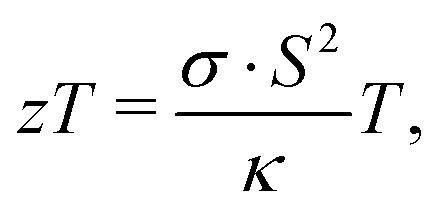
The unique electronic,1–7 optoelectronic8,9 and thermal properties10 of two-dimensional (2D) van der Waals layered transition metal dichalcogenides such as MoS2 have led to a keen interest in this material over the last decade. Moreover, 2D transition metal dichalcogenides have emerged as promising compounds for energy11 applications such as energy generation or conversion. Notably, MoS2 has recently been investigated for prospects in thermoelectricity on both the theoretical12–17 and experimental side.7,18–20The thermoelectric performance of a material is characterized by the dimensionless figure of merit zT:
 | (1) |
![[thin space (1/6-em)]](https://www.rsc.org/images/entities/char_2009.gif) 21 for the suspended monolayer to 84 W m−1 K−1.22 Note that the κ measurement in this 2D material is very challenging and there is a large dispersion of experimental values, see also ref. 23–25 for instance. In addition, the PF for pristine MoS2 may be as high as 2.8 × 10⁴ μW K−2 m−1.16
21 for the suspended monolayer to 84 W m−1 K−1.22 Note that the κ measurement in this 2D material is very challenging and there is a large dispersion of experimental values, see also ref. 23–25 for instance. In addition, the PF for pristine MoS2 may be as high as 2.8 × 10⁴ μW K−2 m−1.16
However, depending on the synthesis technique, exfoliated 2D materials may contain a high density of defects. In MoS2 the defect considered as the most prevalent is sulfur vacancies.26,27 Actually, the defect concentration on freshly exfoliated MoS2 is observed to be as large as 8%.28 This obviously raises the question of the implication of these defects on the physical properties of MoS2 that is not yet well understood from both the experimental and theoretical point of view. For instance, it has a high impact on the performance of field effect transistors29 and several attempts have been made to tune the physical properties through defect engineering.30–32 Regarding the thermal properties, non-equilibrium molecular dynamics calculations have shown a remarkable suppression of the thermal conductivity by point defects in MoS2 nanoribbons.33 Such defects induce the localization of phonon modes and a reduction of thermal conductivity due to an enhancement in Umklapp scattering.34,35 Furthermore, first principle studies have pointed out that the zT may be as high as 6.24 for MoS2 with S defects at room temperature.36 The understanding of the interplay between Umklapp processes and defect scattering is still an open and complex issue that implies a realistic treatment of the disordering and thus of the Anderson localization phenomenon.
In this paper, we address the influence of sulfur vacancies on the thermoelectric properties of single layered hexagonal MoS2 by means of ab initio calculations combined with the Green's function technique and Landauer formalism. We provide an insight into the influence of these defects on the figure of merit zT. The goal is to take into account the natural disordering of sulfur vacancies to investigate the competitive influence of these types of defects on both the power factor and thermal conductivity.
2 Results and discussions
2.1 Theoretical background and methodology
All the calculations are performed using the ab initio package SIESTA37 under the generalized gradient approximation of Perdew, Burke & Ernzerhof38 and using Troullier–Martin norm-conserving pseudopotentials.39 The basis used for the calculations corresponds to a double-zeta-polarized basis optimized using the simplex tool of the package. All the atomic structures were optimized up to forces less than 10−4 eV Å−1. A Monkhorst–pack grid of 10 × 10 × 1 k-points has been used for the calculations. For the Hartree potential, a mesh cutoff of 1000 Ry has been applied which corresponds to a typical mesh size of 0.1 Bohr. This very small mesh size is needed in order to obtain the required accuracy for the dynamical matrix.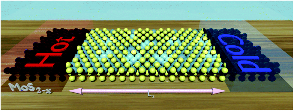 | ||
| Fig. 1 Artwork of a MoS2 monolayer within the Landauer formalism. The leads correspond to pristine MoS2 and the device (between the two leads) corresponds to MoS2 with randomly located sulfur vacancies. | ||
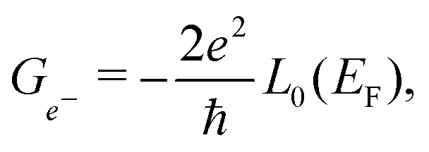
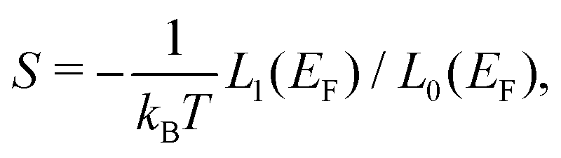
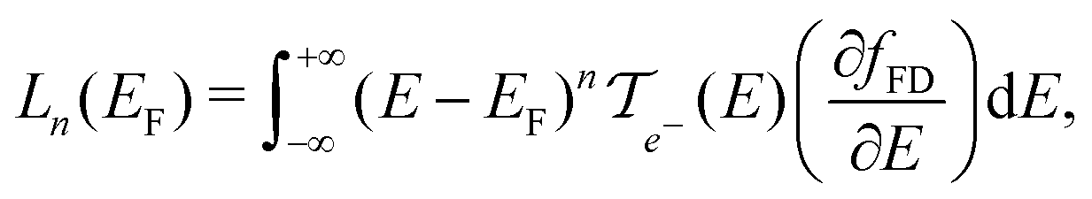
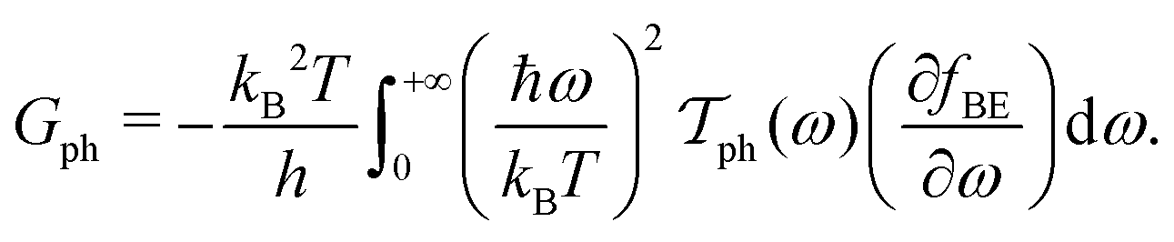
In the framework of Landauer formalism,40–42 the system is divided into two semi-infinite leads and a device (Fig. 1) which includes sulfur vacancies randomly located. The leads correspond to pristine MoS2 (no vacancy). The thermoelectric properties i.e. the Seebeck coefficient, electrical conductance and thermal conductance are computed using the transmission coefficients through the system for the electrons and the phonons. These transmissions are obtained thanks to the Green's functions of the system which are built either from the Hamiltonian (electrons) or the dynamical matrix (phonons). These last operators are obtained from the ab initio calculations. This approach is a very efficient way to deal with defects and provides an insight into the effect of sulfur vacancies on the transport properties. The electrical conductance, the Seebeck coefficient and the thermal conductance are defined as follows:
 | (2a) |
 | (2b) |
 | (2c) |
 | (2d) |
In these equations, e is the electron charge, ħ is the reduced Planck constant, kB is the Boltzmann constant, T is the temperature, EF is the Fermi energy of the system, fFD(E) is the Fermi–Dirac distribution and fBE(ω) is the Bose–Einstein distribution.  and
and  are, respectively, the electron and phonon transmissions. The equation which defines the phonon thermal conductance involves the derivative of the Bose–Einstein distribution. This derivative (depicted in Fig. 2) figures the respective weight of each conduction channel in conductance. The electronic contribution to the thermal conductance can be defined in a similar way (see ref. 43). However, this contribution is negligible when compared to the lattice contribution as pointed out in ref. 44 and 45. At least 99% of the heat conduction happens through the lattice at room temperature. This behavior is attributed to the small density of states near the Fermi level.
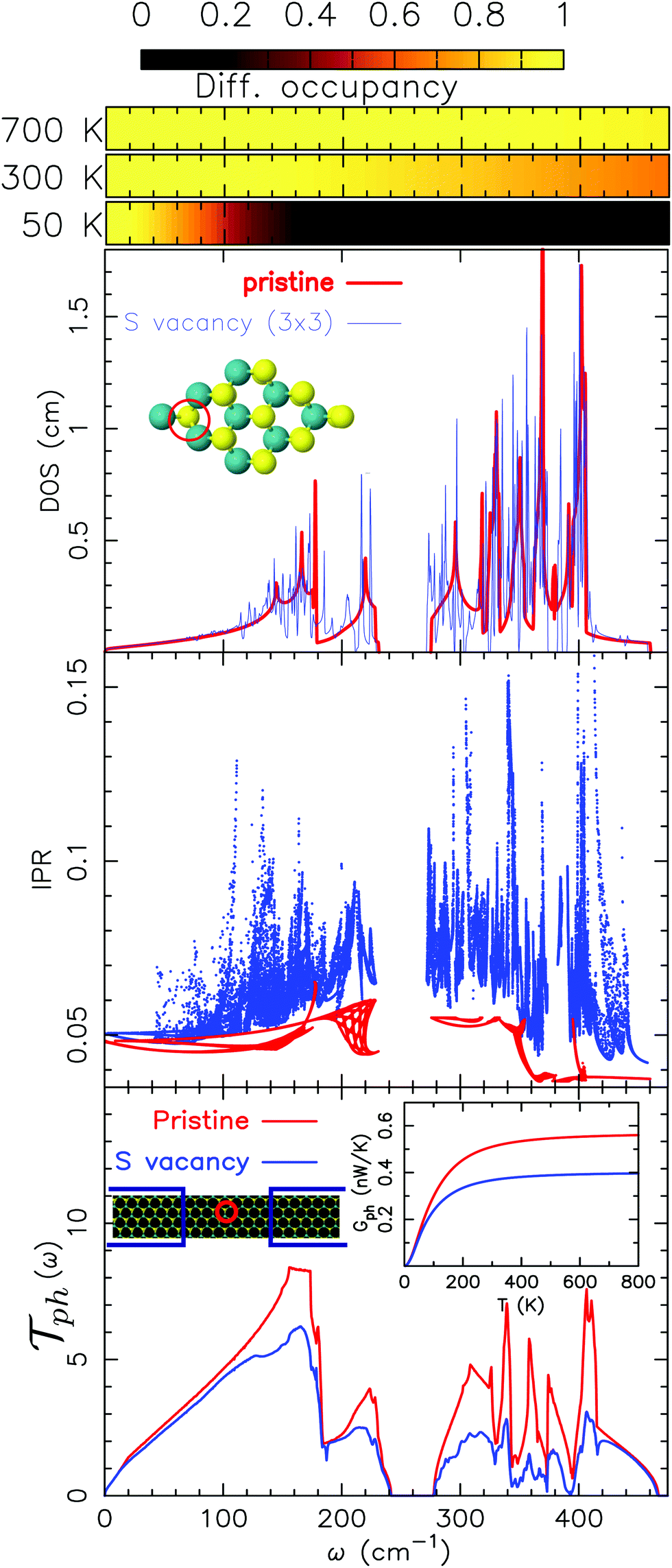 | ||
| Fig. 2 From top to bottom: Normalized differential occupancy of the Bose–Einstein distribution (as defined in eqn (4)), phonon density of states for a 3 × 3 cell either for pristine MoS2 or with a sulfur vacancy, the inverse participation ratio (as defined in eqn (5)) and phonon transmission for pristine MoS2 and a device with a single sulfur vacancy. All of them are given as functions of the energy of the phonon modes. | ||
On the basis of the Landauer–Büttiker formalism, the transmission reads:41
 | (3) |
2.2 Phonon transport with a single sulfur vacancy
In Fig. 2, the behavior of MoS2 with a single sulfur vacancy is presented either under periodic boundary conditions or isolated using Landauer formalism. These basic models are intended to pinpoint the effects associated with a defect and to facilitate the interpretation of the more realistic results presented hereafter when defects are randomly located. On top of this figure is pictured the normalized differential occupancy of the Bose–Einstein distribution defined as: | (4) |
This quantity is involved in the integral (cf.eqn (2d)) defining the thermal conductance and characterizes the occupancy of the conduction channels. Notably, at low temperature (50 K) only the low frequency acoustic modes are involved in the transport. Conversely, at room and higher temperatures, all the acoustic modes are involved along with the optical ones. This is consistent with the estimated average acoustic Debye temperature in MoS2 that is of the order of 260 K (see also ref. 47).
One issue of concern is the localization of the phonon modes induced by the vacancy. This effect can clearly be pointed out by considering the inverse participation ratio (IPR) that reads:
 | (5) |
The role of an isolated vacancy in the transport properties is actually linked with the previous remark. When we compare the transmission between the pristine case and that of the one with a sulfur vacancy, it is mainly the in-plane optical modes that are affected by the defect. More remarkably, the in plane optical modes (in the frequency range from 250 cm−1 to 420 cm−1, see Fig. 7) are the most scattered modes in contrast to the ZO modes (above 420 cm−1) that are almost unaffected. Despite the rather high frequency of LO–TO modes, this has a significant influence on the thermal conductance (see the inset of Fig. 2). Indeed, the thermal conductance defined by means of the phonon transmission in eqn (2d) involves the derivative of the Bose–Einstein distribution. This derivative is represented on top of Fig. 2. Given that the spectrum range of MoS2 is rather narrow (compared to graphene,48 for instance), almost all the conduction modes (acoustic and optical) are involved in the transport at room temperature. The direct consequence, when mixed with the scattering of the optical modes, is a reduction in conductance by almost one-third at room temperature compared to that of the pristine case.
2.3 Electronic transport with a single sulfur vacancy
As mentioned in the theoretical section, we need to deal with both the thermal and electronic properties to estimate the zT. Thus, in this section we address the influence of a single sulfur vacancy on the electronic transport properties of MoS2. The main aim is to provide an insight into the influence of such defect.In Fig. 3, the fundamental difference between a calculation done on a periodic system and a disordered one is pointed out. On top of this figure, the electronic density of states for a 3 × 3 periodic cell with a sulfur vacancy is given. This vacancy induces specific bands within the band gap of the material. These bands are less dispersed and one is fully occupied.49 However, the occurrence of these bands is closely related to their periodicity. This is illustrated in the transmission. We have either considered a system with a sulfur vacancy repeated periodically (each unit cell corresponds to (MoS1,958)24) or a device (with a length Lz of 13 nm) on which the vacancies are randomly distributed.† Note that both of them have the same vacancy density. For the periodic case the bands induced by the vacancy lead to well defined conduction channels. However, periodic defects are not realistic and it can clearly be seen that for the disordered system these channels are almost fully suppressed (note the logarithmic scale). This means that it is only the native bands of the material (not the ones induced by the vacancy) which can play a role in the transport. This is compatible with the experimental observations of a variable range hopping50,51 and also with STM measurements.52
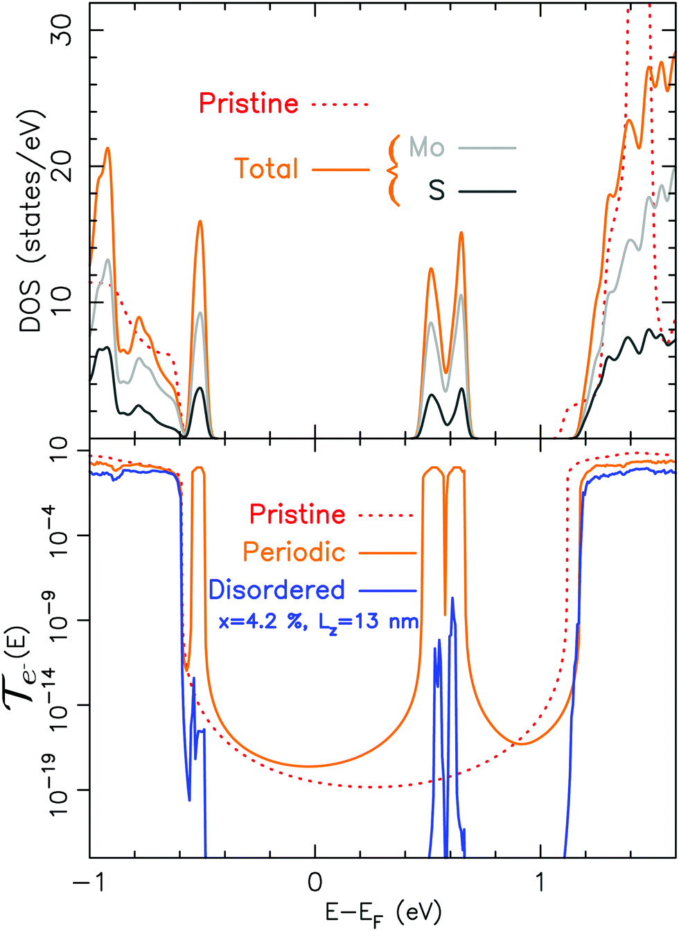 | ||
| Fig. 3 From top to bottom: Electronic density of states for a 3 × 3 MoS2 cell with a sulfur vacancy and electronic transmission for a device with sulfur vacancies either periodic or randomly located (disordered). Both of them are represented as functions of energy (centered at the Fermi level). For the transmission, x is the vacancy density defined as MoS2−x. | ||
Fig. 4 depicts the electrical conductance, the Seebeck coefficient and the PF (at 300 K and 700 K) either in pristine MoS2 or in a compound with a single sulfur vacancy. Here, we have considered a rigid band shift model, wherein the position of the Fermi level is shifted rigidly either toward the valence band or towards the conduction band to mimic hole or electron doping, respectively. The dashed lines correspond to the positions of the Fermi level for which the PF is maximum. In what follows, zT will be estimated for the electron/hole density that maximizes the PF. Let us now focus on the energy range that is relevant for the transport properties. Note that only narrow regions close to the top of the valence band and to the bottom of the conduction band are relevant to the transport. These energy windows result from the derivative of Fermi distribution involved in the equations that define the Seebeck coefficient and the electrical conductance (see eqn (2b) and (2a)). This is illustrated in the inset of Fig. 4 representing the transmission. The shaded green regions represent the energy windows around the Fermi level that have a significant weight for the transport at 700 K. Of course, at room temperature, these windows are about two times smaller.
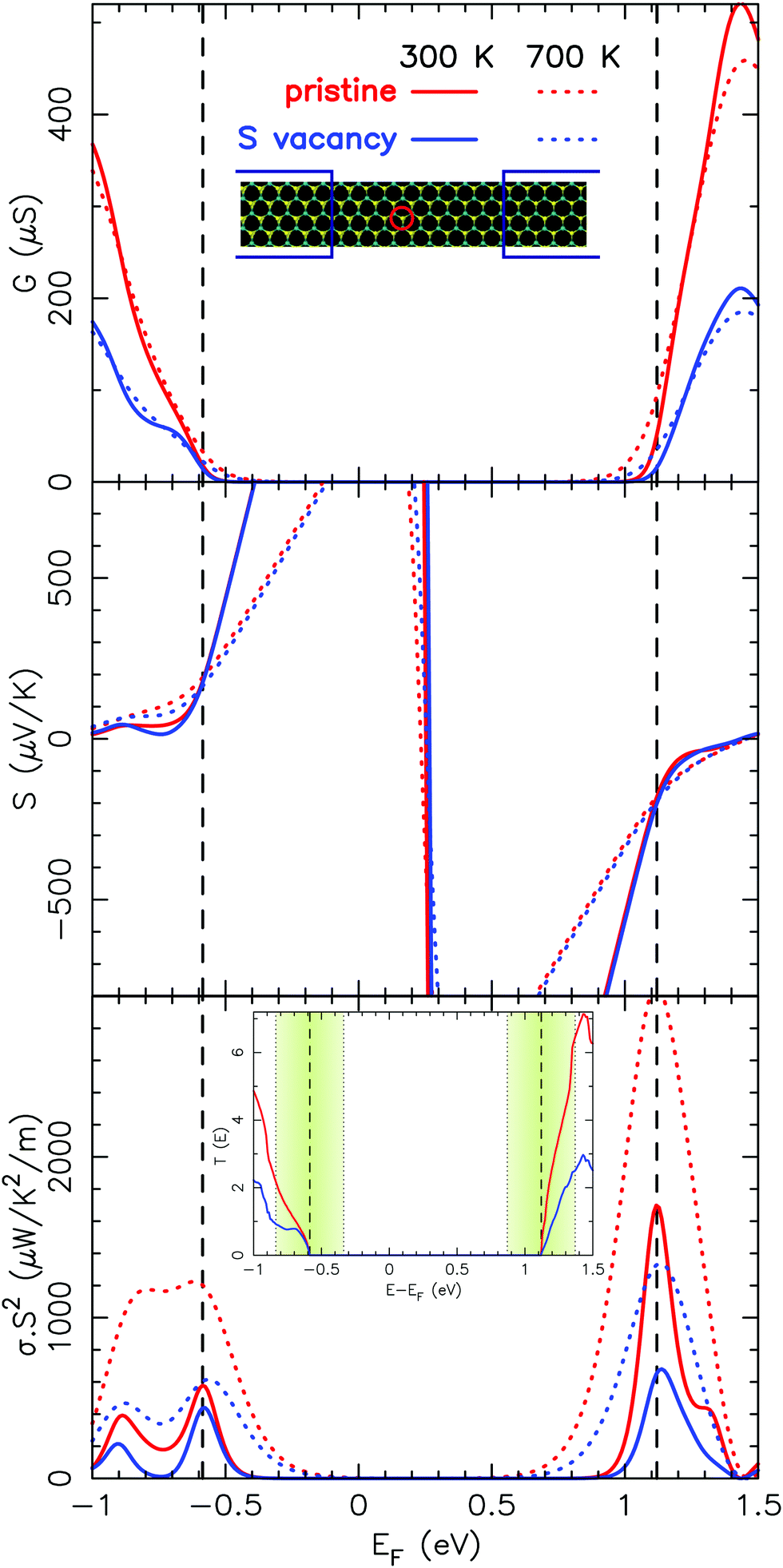 | ||
| Fig. 4 From top to bottom: Electrical conductance, the Seebeck coefficient and the power factor for pristine MoS2 and MoS2 with a single sulfur vacancy as functions of the Fermi level at either 300 K or 700 K. The inset of the power factor depicts the corresponding transmission coefficients along with the illustration of the relative weight at 700 K (in shaded green) of the conduction channels in the conductance at the maximum of the power factor either for the valence or the conduction band. | ||
Regarding the valence band, the influence of the sulfur vacancy is significant only at low energy (with respect to the top of the valence band). For this reason, the impact on the maximum of the PF (when compared to the pristine case) is modest at room temperature but clearly noticeable at 700 K. At this temperature, the PF obtained with the defect is 2 times smaller than that of the pristine case. Conversely, the influence of the defect on the conduction band is noticeable until the very bottom of the band. Thus, for n-type doping, the decrease of the PF is much more important and significant whatever the temperature is. As presented hereafter this trend is also observed in disordered systems. One should note that the Seebeck coefficient is almost unaffected by the defect and the observed variations of the PF are mainly due to the variations of the electrical conductance.
To explain the different impact of the sulfur vacancy on the valence and conduction bands, one should keep in mind that the first nearest neighbors of the S vacancy are Mo atoms. In addition, the projected DOS of MoS2 (see, for instance, ref. 53) consists mainly of Mo d-type contribution for the bottom of the conduction band, and a mix of Mo d-type and S p-type contributions for the top of the valence band. Indeed, the vacancy modifies significantly the onsite potential experienced by the Mo atoms in contrast to its weakest effect on the onsite potential experienced by S atoms.‡ Hence, scattering is expected to be stronger for the states at the bottom conduction band than for those at the top of the valence band.
2.4 Figure of merit in disordered MoS2−x
Let us proceed further and consider now the more realistic case of finite concentration of sulfur vacancies and its effect on the zT. To this end, we have considered systems composed of 2 pristine MoS2 leads connected to a device where the sulfur vacancies are randomly located with a given vacancy concentration x. In this section, all the results correspond to an average over 10 different compounds with the random distribution of the vacancies. This gives us results with a typical standard deviation smaller than the size of the symbols used in the figures. We have considered vacancy densities ranging from 0.8% to 4.2% that correspond to surfacic densities ranging from 9.7 × 1012 cm−2 to 4.9 × 1013 cm−2. Note that these values agree well with the typical densities measured experimentally.27Fig. 5 depicts the transmission coefficients for both phonons and electrons (the valence and the conduction bands are shown separately). These transmissions are given for the increasing length of the device i.e. the region that contains the defects. Regarding the phonon transport, it is the in-plane optical modes that are most affected by the vacancies as previously observed in the single vacancy case. As can be clearly seen, for the increasing length of the system, the in plane optical channels are almost fully suppressed. In contrast, both the acoustic and ZO modes (out of plane optical modes at frequencies above 400 cm−1, see Fig. 7) are weakly affected by the vacancies. The reduction in thermal conductivity§ as seen in the inset of Fig. 5 reflects the suppression of the in-plane optical modes (especially at room and higher temperatures) by multiple scattering on S vacancies. It should be emphasized that here the calculation of the conductivity includes phonon–phonon Umklapp scattering via the mode Grüneisen parameters (see, for instance, ref. 54). The details of the procedure are given in Section 4. A more refined study based on the calculations of third order interatomic force constants may be found in ref. 55. However, the device lengths considered here are of the same order of magnitude of the typical mean free path associated with phonon–phonon Umklapp scattering (as shown in Fig. 10). For this reason its effect is less and the associated reduction of the conductivity at high temperature is only noticeable for the longest system size. Nonetheless, the comparison of κ for pristine and defective MoS2 clearly shows that, for this device size, the main mechanism of the reduction of κ is scattering by the defects. This suggests that the length scale on which phonons are scattered by the defects is smaller than the Umklapp one. Furthermore, note the good quantitative agreement for κ between our calculations and experimental values. Indeed, we find, respectively, 90 W m−1 K−1 for the pristine case and 12 W m−1 K−1 for the 3.3% defective compound to be compared with the experimental data which range from 13.3 W m−1 K−1 to 84 W m−1 K−1.21,22 This corroborates our analysis on the competitive influence of Umklapp and defect scattering. The typical length scales that control the transport properties are further discussed in what follows.
 | ||
| Fig. 5 Transmission coefficient for phonons (left) or electrons (right) as a function of either frequency or energy for a system containing 3.3% of sulfur vacancies and for 3 different lengths. In the inset of the phonon transmission is given the thermal conductivity as a function of temperature for both defective and pristine compounds. | ||
Regarding electron transport, the conduction band (n-doping) is impaired the most by the vacancies, especially at the bottom of the band which is the energy spot of interest when computing the power factor. A backscattering is also noticeable for p-doping. However, at the top of the valence band (the region of interest for the PF), the influence of the vacancies is less crucial. As presented hereafter, this difference in behavior between n and p-type doping has a direct repercussion on zT.
The figure of merit is the result of the antagonist effects of the thermal and electron transport properties associated with κ and the PF. If κ is less altered than the PF, the zT will be low and conversely, if κ is more altered than the PF, the zT will be large. Actually, depending on the sulfur vacancy concentration and on the type of doping (n or p), the two situations are encountered. Fig. 6 depicts the figure of merit for n and p-type MoS2 with different vacancy concentrations. For p-type doping the system is relatively insensitive to defects. At room temperature the zT remains constant as we vary the system length. This means that the combined effects of the vacancies on κ and on the PF compensate each other. It is only at high temperature (700 K) that the PF decreases more rapidly than κ, leading to a reduction in the zT with the system size. This trend originates from the integration window in eqn (2a) and (2b) defining G and S. Its width increases with temperature and at 700 K it includes an area on which the transmission for the valence band is significantly reduced by the defects. However, the zT is nonetheless of the order of 0.5. On the other hand, for n-type doping, the picture is drastically different. The zT decreases very rapidly with the length of the system. At room temperature it drops to almost negligible values especially at large vacancy concentration. It is only at low concentration that the zT has more attractive values. At higher temperature the zT reaches values of the same magnitude than those obtained for p-type doping. However, a rapid decrease of the zT with the length is still observed. This behavior is related to the large influence of the sulfur vacancies on the conduction band, and hence on the PF. For pristine MoS2, the conduction band is supposed to lead to a larger PF than the valence band. This does not go well with sulfur vacancies which wipe out the conduction channels. Therefore the only way to maintain a significant zT for n-type doping is to have a very low vacancy concentration.
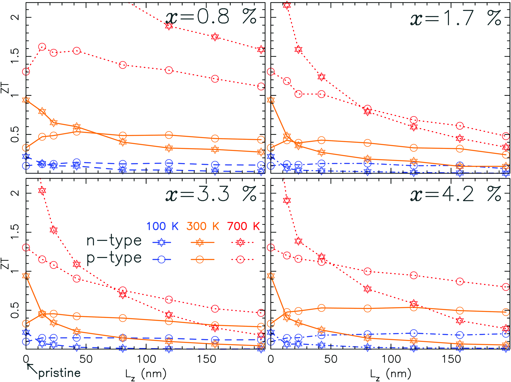 | ||
| Fig. 6 Figure of merit as a function of the length of the system for 4 different sulfur vacancy concentrations and 3 different temperatures. Note that the values at Lz = 0 correspond to the pristine case. | ||
The behavior of the zT portrayed previously is closely related to the decay with the system size of both the PF and thermal conductivity. This behavior is illustrated in Fig. 9 for the PF and a similar behavior is observed for κ (not shown). Indeed, the PF and thermal conductivity follow an exponentially decreasing trend with the length. The characteristic lengths, denoted as LPF for the PF and Lκ for κ, are associated with the localization length56 of the electron eigenstates (respectively phonon modes). LPF and Lκ as functions of temperature are summarized in Table 1. As expected, LPF is significantly larger for p-type than for n-type doping whatever the temperature. In addition, these lengths are typically of the order of 55 nm for n-type doping and 100 nm for p-type doing. Moreover, Lκ is always larger than LPF. This is directly reflected in the rapid decrease of the zT with the length of the device reported previously. Note that this decaying length scale is almost insensitive to temperature. As discussed previously, these features are consistent with the fact that the scattering lengths associated with the defects are smaller than those of the Umklapp processes. Let us further discuss the competition between LPF and Lκ for p-type doping. At 100 K (and in a few instances at 300 K) the 2 lengths are almost equivalent leading to a zT almost constant with the device size as illustrated in Fig. 6. In contrast, at 700 K, LPF becomes much smaller causing a rapid drop in the zT.
| L PF (nm) | L κ (nm) | ||
|---|---|---|---|
| n-Type | p-Type | ||
| 100 K | 31 | 129 | 159 |
| 300 K | 58 | 107 | 150 |
| 700 K | 53 | 88 | 146 |
3 Conclusion
In this paper we have addressed, on the basis of ab initio calculations and Landauer formalism, the effects of sulfur vacancies on the thermoelectric properties of single layered hexagonal MoS2. We have investigated both the phonon and electron transport properties of this material by treating the disorder effects realistically. It appears that in plane phonon optical modes are very sensitive to sulfur vacancies and are more likely to be scattered by them. However, the mechanism which is governing the thermoelectric figure of merit is mostly linked with the PF. For p-type doping the electronic transport properties are less impaired by S vacancies. This leads to a zT almost independent of the length of the system and of the vacancy concentrations. Conversely, for n-type doping, scattering is massive and it leads to a drastic reduction in the zT. These features are related to typical decaying length scales for both the PF and κ revealing that scattering with the vacancies is a dominant mechanism in these disordered systems.4 Supplementary data
In Fig. 7, the phonon dispersion for 2D MoS2 is given. The acoustic out of plane mode (ZA) has the typical parabolic shape of a 2D material at the Γ point corresponding to the in plane modes (LA and TA). The optical out of plane modes (denoted as A1′ and A2′′) are well separated from the other modes at the top of the dispersion between 400 and 470 cm−1.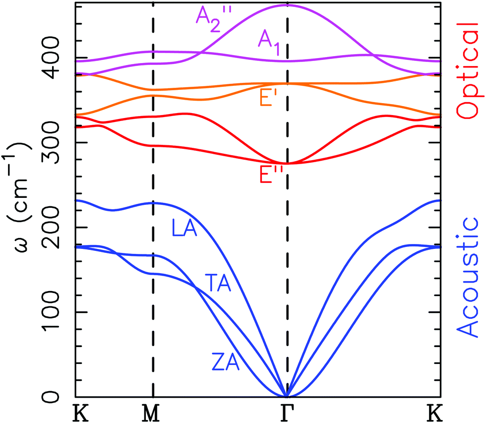 | ||
| Fig. 7 Phonon dispersion modes for two dimensional MoS2. A1′ and A2′′ are out of plane optical modes (usually represented as ZO), and E′ and E′′ are in plane optical modes. | ||
The amplitude of the PF strongly depends on the Fermi level. Indeed, the PF is the product of σ and the square of S which have two opposite trends with the Fermi level. This leads to a bell-shaped function for the PF with a maximum at a given optimal Fermi level (see Fig. 4). The zT, as shown in Fig. 6, is evaluated using the maximum value of the PF. This choice is definitely an open issue as it would result in tuning each vacancy concentration, temperature and length of the system at the optimal Fermi level. In Fig. 8 we have compared the zT (with a vacancy concentration of 4.2%) using either the optimal Fermi level (as in Fig. 6) or a fixed Fermi level close to the top (bottom) of the valence (conduction) band, respectively. For each type of doping, we considered two different values at the Fermi level. These values are in close vicinity of the maximum of the PF obtained for the pristine case (see Fig. 4). As expected, a fixed Fermi level is leading to smaller values of the zT as the PF is not at its maximum. However, the trends pointed out in Section 2.4 for the zT with the length are not affected. For n-type doping the deviation from the optimal case is of the order of 0.2. Indeed, for n-type doping, the optimal Fermi level is almost constant (ranging from 1.14 eV to 1.16 eV) regardless of the length and the temperature of the system. For p-type doping, the optimal Fermi level varies a bit more with the length and mainly with the temperature. This leads to larger deviations of the zT. At 100 K, the optimal Fermi level is −0.61 eV and at 700 K it is −0.51 eV which is much closer to the top of the valence band.
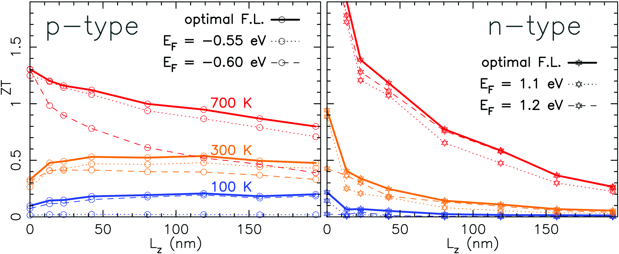 | ||
| Fig. 8 Figure of merit as a function of the length of the system for a sulfur vacancy concentration of 4.2% and 3 different temperatures. The solid lines correspond to the optimal Fermi level (giving rise to the maximum of the PF and hence of the zT). The dashed and dotted lines correspond to a fixed Fermi level. | ||
Fig. 9 gives the PF as a function of the length of the system. It is computed using a rigid band shift model. These values correspond to the maximum of the PF (as illustrated in Fig. 4). The electrical conductivity is defined as σ = G/Ly where Ly is the thickness of the layer (typically 6.4 Å). Beyond 50 nm, the PF follows a typically exponentially decreasing trend with a characteristic length LPF56i.e. it follows a decay law of the form e−Lz/LPF.
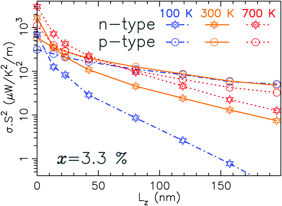 | ||
| Fig. 9 Power factor for n-type and p-type MoS2−x (x = 3.3%) as a function of the length of the device and for 3 different temperatures. | ||
To include the effect of Umklapp scattering, we have made an assumption that the scattering of the phonons by the defects (sulfur vacancies) and the phonon–phonon Umklapp processes are uncorrelated. With this assumption, the phonon transmission coefficient is defined as follow:
 | (6) |
 is the phonon transmission coefficient which includes scattering by the defects (x is the direction perpendicular to the direction of transport) and
  is the mean free path (averaged over qz) associated with phonon–phonon Umklapp scattering. This integral is obtained using 400 discrete points for qx. The fraction involving Lz and
  in this equation is introduced to have a continuity between the ballistic and the diffusive regime. If
  the fraction tends to
  and if
  it tends to 1 which corresponds to a ballistic regime for the Umklapp processes. The mean free path per mode is defined using the mode Grüneisen parameter:57
 | (7) |
![[q with combining tilde]](https://www.rsc.org/images/entities/i_char_0071_0303.gif) ) is the group velocity, τα() is the relaxation time, M is the mass of the unit cell, ωmaxα is the Debye frequency, γα() is the Grüneisen parameter and ωα() is the frequency of the mode α. The Grüneisen parameter for the system with a sulfur vacancy is computed using the post-processing tool phonopy.58 In Fig. 10 the group velocity, the phonon lifetime and the mean free path values are shown after computation using eqn (7). The results obtained with a sulfur vacancy correspond to a 3 × 3 cell. As already pointed out in Section 2.2, the vacancy induces a localization of the phonon modes which leads here to a reduction and to a larger dispersion of the values compared to the pristine case.
) is the group velocity, τα() is the relaxation time, M is the mass of the unit cell, ωmaxα is the Debye frequency, γα() is the Grüneisen parameter and ωα() is the frequency of the mode α. The Grüneisen parameter for the system with a sulfur vacancy is computed using the post-processing tool phonopy.58 In Fig. 10 the group velocity, the phonon lifetime and the mean free path values are shown after computation using eqn (7). The results obtained with a sulfur vacancy correspond to a 3 × 3 cell. As already pointed out in Section 2.2, the vacancy induces a localization of the phonon modes which leads here to a reduction and to a larger dispersion of the values compared to the pristine case.
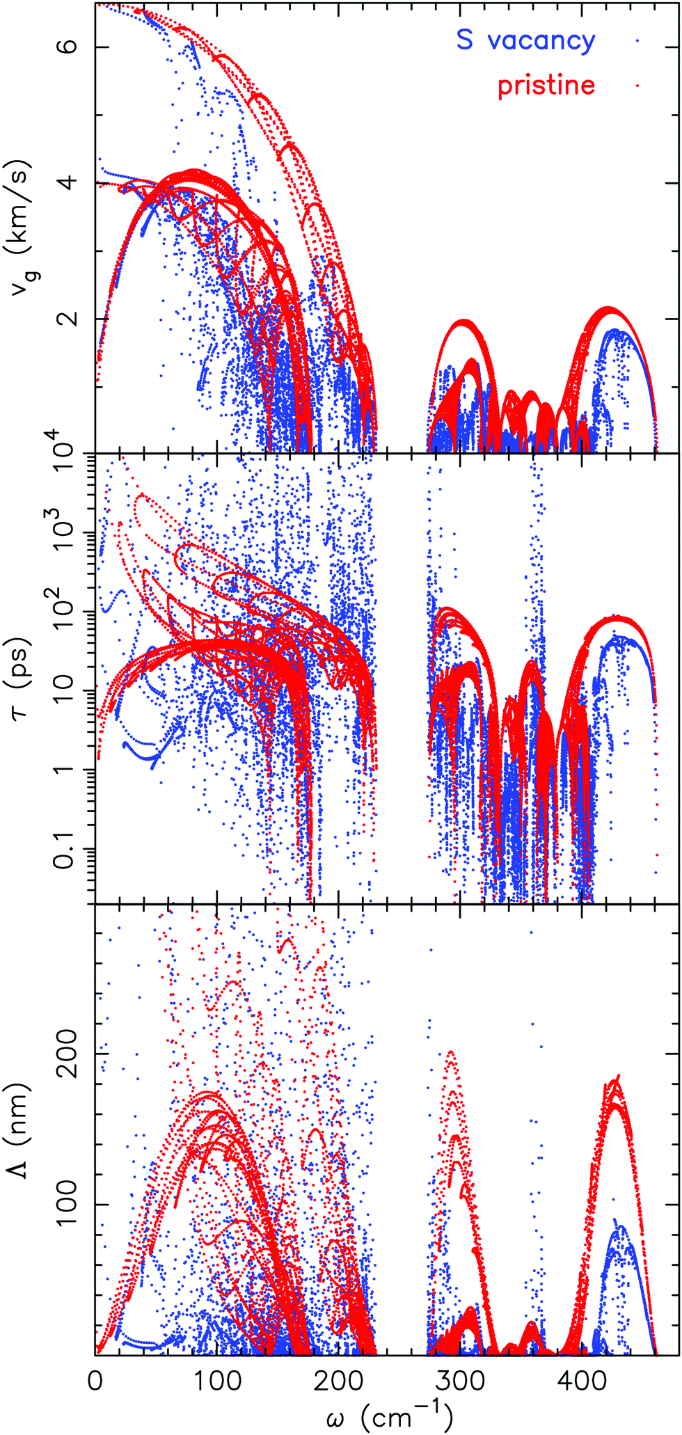 | ||
| Fig. 10 From top to bottom group velocity, phonon lifetime and the mean free path (as computed in eqn (7)) for either pristine MoS2 or for a 3 × 3 cell with a sulfur vacancy. | ||
To obtain  as defined in eqn (6), we average Λ(ωα()) over the reciprocal vector qz (where z is the direction of transport):
 | (8) |
Conflicts of interest
There are no conflicts to declare.Notes and references
- K. F. Mak, C. Lee, J. Hone, J. Shan and T. F. Heinz, Phys. Rev. Lett., 2010, 105, 136805 CrossRef PubMed.
- E. S. Kadantsev and P. Hawrylak, Solid State Commun., 2012, 152, 909–913 CrossRef CAS.
- B. Radisavljevic, A. Radenovic, J. Brivio, V. Giacometti and A. Kis, Nat. Nanotechnol., 2011, 6, 147–150 CrossRef CAS PubMed.
- D. Lembke and A. Kis, ACS Nano, 2012, 6, 10070–10075 CrossRef CAS PubMed.
- S. Das, H.-Y. Chen, A. V. Penumatcha and J. Appenzeller, Nano Lett., 2012, 13, 100–105 CrossRef PubMed.
- M. Buscema, M. Barkelid, V. Zwiller, H. S. J. van der Zant, G. A. Steele and A. Castellanos-Gomez, Nano Lett., 2013, 13, 358–363 CrossRef CAS PubMed.
- J. Wu, H. Schmidt, K. K. Amara, X. Xu, G. Eda and B. Özyilmaz, Nano Lett., 2014, 14, 2730–2734 CrossRef CAS PubMed.
- H. S. Lee, S.-W. Min, Y.-G. Chang, M. K. Park, T. Nam, H. Kim, J. H. Kim, S. Ryu and S. Im, Nano Lett., 2012, 12, 3695–3700 CrossRef CAS PubMed.
- Z. Yin, H. Li, H. Li, L. Jiang, Y. Shi, Y. Sun, G. Lu, Q. Zhang, X. Chen and H. Zhang, ACS Nano, 2012, 6, 74–80 CrossRef CAS PubMed.
- E. Yalon, C. J. McClellan, K. K. H. Smithe, M. MuÃśoz Rojo, R. L. Xu, S. V. Suryavanshi, A. J. Gabourie, C. M. Neumann, F. Xiong, A. B. Farimani and E. Pop, Nano Lett., 2017, 17, 3429–3433 CrossRef CAS PubMed.
- N. Choudhary, M. A. Islam, J. H. Kim, T.-J. Ko, A. Schropp, L. Hurtado, D. Weitzman, L. Zhai and Y. Jung, Nano Today, 2018, 19, 16–40 CrossRef CAS.
- Z. Jin, Q. Liao, H. Fang, Z. Liu, W. Liu, Z. Ding, T. Luo and N. Yang, Nat. Sci. Rep., 2015, 5, 18342 CrossRef CAS PubMed.
- W. Huang, H. Da and G. Liang, Thermoelectric performance of MX2 (M = Mo,W; X = S,Se) monolayers, J. Appl. Phys., 2013, 113, 104304 CrossRef.
- W. Huang, X. Luo, C. K. Gan, S. Y. Quek and G. Liang, Theoretical study of thermoelectric properties of few-layer MoS2 and WSe2, Phys. Chem. Chem. Phys., 2014, 16, 10866–10874 RSC.
- D. D. Fan, H. J. Liu, L. Cheng, P. H. Jiang, J. Shi and X. F. Tang, Appl. Phys. Lett., 2014, 105, 133113 CrossRef.
- H. Babaei, J. M. Khodadadi and S. Sinha, Appl. Phys. Lett., 2014, 105, 193901 CrossRef.
- R.-N. Wang, G.-Y. Dong, S.-F. Wang, G.-S. Fua and J.-L. Wang, Phys. Chem. Chem. Phys., 2017, 19, 5797–5805 RSC.
- M. Yoshida, T. Iizuka, Y. Saito, M. Onga, R. Suzuki, Y. Zhang, Y. Iwasa and S. Shimizu, Nano Lett., 2016, 16, 2061–2065 CrossRef CAS PubMed.
- T. Wang, C. Liu, J. Xu, Z. Zhu, E. Liu, Y. Hu, C. Li and F. Jiang, Nanotechnology, 2016, 27, 285703 CrossRef PubMed.
- K. Hippalgaonkar, Y. Wang, Y. Ye, D. Y. Qiu, H. Zhu, Y. Wang, J. Moore, S. G. Louie and X. Zhang, Phys. Rev. B, 2017, 95, 115407 CrossRef.
- J. J. Bae, H. Y. Jeong, K. H. Han, J. Kim, H. Kim, M. S. Kim, B. H. Moon, S. C. Lim and Y. H. Lee, Nanoscale, 2017, 9, 2541–2547 RSC.
- X. Zhang, D. Sun, Y. Li, G.-H. Lee, X. Cui, D. Chenet, Y. You, T. F. Heinz and J. C. Hone, ACS Appl. Mater. Interfaces, 2015, 7(46), 25923–25929 CrossRef CAS PubMed.
- R. Yan, J. R. Simpson, S. Bertolazzi, J. Brivio, M. Watson, X. Wu, A. Kis, T. Luo, A. R. Hight Walker and H. G. Xing, ACS Nano, 2014, 8, 986–993 CrossRef CAS PubMed.
- S. Sahoo, A. P. S. Gaur, M. Ahmadi, M. J.-F. Guinel and R. S. Katiyar, J. Phys. Chem. C, 2013, 117, 9042–9047 CrossRef CAS.
- A. Taube, J. Judek, A. Łapińska and M. Zdrojek., ACS Appl. Mater. Interfaces, 2015, 7, 5061–5065 CrossRef CAS PubMed.
- W. Zhou, X. Zou, S. Najmaei, Z. Liu, Y. Shi, J. Kong, J. Lou, P. M. Ajayan, B. I. Yakobson and J.-C. Idrobo, Nano Lett., 2013, 13, 2615–2622 CrossRef CAS PubMed.
- J. Hong, Z. Hu, M. Probert, K. Li, D. Lv, X. Yang, L. Gu, N. Mao, Q. Feng, L. Xie, J. Zhang, D. Wu, Z. Zhang, C. Jin, W. Ji, X. Zhang, J. Yuan and Z. Zhang, Nat. Commun., 2015, 6, 6293 CrossRef CAS PubMed.
- R. Addou, S. McDonnell, D. Barrera, Z. Guo, A. Azcatl, J. Wang, H. Zhu, C. L. Hinkle, M. Quevedo-Lopez, H. N. Alshareef, L. Colombo, J. W. P. Hsu and R. M. Wallace, ACS Nano, 2015, 9, 9124–9133 CrossRef CAS PubMed.
- B. Stampfer, F. Zhang, Y. Y. Illarionov, T. Knobloch, P. Wu, M. Waltl, A. Grill, J. Appenzeller and T. Grasser, ACS Nano, 2018, 12, 5368–5375 CrossRef CAS PubMed.
- Y. Chen, S. Huang, X. Ji, K. Adepalli, K. Yin, X. Ling, X. Wang, J. Xue, M. Dresselhaus, J. Kong and B. Yildiz, ACS Nano, 2018, 12, 2569–2579 CrossRef CAS PubMed.
- H. Zuyun, Z. Ran, C. Xiaofei, C. Huijun, Z. Yunmin, S. Huimin, H. Shengxi, X. Jianming, D. Junfeng, C. Shuang, L. Meilin, W. Xinwei and Y. Chen, ACS Appl. Mater. Interfaces, 2018, 10, 42524–42533 CrossRef PubMed.
- D. Saha and S. Mahapatra, J. Appl. Phys., 2016, 119, 134304 CrossRef.
- Y. Wang, K. Zhang and G. Xie, Appl. Surf. Sci., 2016, 360, 107–112 CrossRef CAS.
- B. Peng, Z. Ning, H. Zhang, H. Shao, Y. Xu, G. Ni and H. Zhu, J. Phys. Chem. C, 2016, 120, 29324–29331 CrossRef CAS.
- Z. Ding, Q.-X. Pei, J.-W. Jiang and Y.-W. Zhang, J. Phys. Chem. C, 2015, 119, 16358–16365 CrossRef CAS.
- M. Sharma, A. Kumar and P. Ahluwalia, Phys. E, 2019, 107, 117–123 CrossRef CAS.
- J. M. Soler, E. Artacho, J. D. Gale, A. García, J. Junquera, P. Ordejón and D. Sánchez-Portal, J. Phys.: Condens. Matter, 2002, 14, 2745–2779 CrossRef CAS.
- J. P. Perdew, K. Burke and M. Ernzehof, Phys. Rev. Lett., 1996, 77, 3865–3868 CrossRef CAS PubMed.
- N. Troullier and J. L. Martins, Phys. Rev. B: Condens. Matter Mater. Phys., 1991, 43, 1993–2006 CrossRef CAS PubMed.
- S. Datta, Electronic transport in mesoscopic systems, Cambridge University Press, Cambridge, UK, 1995 Search PubMed.
- M. Brandbyge, J.-L. Mozos, P. Ordejón, J. Taylor and K. Stokbro, Phys. Rev. B: Condens. Matter Mater. Phys., 2002, 65, 165401 CrossRef.
- W. Zhang, T. S. Fisher and N. Mingo, The atomistic green's function method: An efficient simulation approach for nanoscale phonon transport, Numer. Heat Transfer, Part B, 2007, 51(4), 333–349 CrossRef CAS.
- C. Jeong, R. Kim, M. Luisier, S. Dattaand and M. Lundstrom, J. Appl. Phys., 2010, 107, 023707 CrossRef.
- A. Naidu Gandi and U. Schwingenschlögl, EPL, 2016, 113, 36002 CrossRef.
- X. Meng, T. Pandey, J. Jeong, S. Fu, J. Yang, K. Chen, A. Singh, F. He, X. Xu, J. Zhou, W.-P. Hsieh, A. K. Singh, J.-F. Lin and Y. Wang., Phys. Rev. Lett., 2019, 122, 155901 CrossRef CAS PubMed.
- C. Adessi, S. Roche and X. Blase, Phys. Rev. B: Condens. Matter Mater. Phys., 2006, 73, 125414 CrossRef.
- B. Peng, H. Zhang, H. Shao, Y. Xu, X. Zhang and H. Zhu, RSC Adv., 2016, 6, 5767–5773 RSC.
- D. L. Nika and A. A. Balandin, J. Phys.: Condens. Matter, 2012, 24, 233203 CrossRef PubMed.
- A. V. Krivosheeva, V. L. Shaposhnikov, V. E. Borisenko, J.-L. Lazzari, C. Waileong, J. Gusakova and B. K. Tay, J. Semicond., 2015, 36, 122002 CrossRef.
- S. Ghatak, A. N. Pal and A. Ghosh, ACS Nano, 2011, 5, 7707–7712 CrossRef CAS PubMed.
- H. Qiu, T. Xu, Z. Wang, W. Ren, H. Nan, Z. Ni, Q. Chen, S. Yuan, F. Miao, F. Song, G. Long, Y. Shi, L. Sun, J. Wang and X. Wang, Nat. Commun., 2013, 4, 2642 CrossRef PubMed.
- P. Vancsó, G. Z. Magda, J. Petö, J.-Y. Noh, Y.-S. Kim, C. Hwang, L. P. Biró and L. Tapasztó, Sci. Rep., 2016, 6, 29726 CrossRef PubMed.
- E. S. Kadantsev and P. Hawrylak, Solid State Commun., 2012, 152, 909–913 CrossRef CAS.
- W.-X. Zhou and K.-Q. Chen, Sci. Rep., 2015, 5, 15070 CrossRef CAS PubMed.
- W. Li, J. Carrete and N. Mingo, Appl. Phys. Lett., 2013, 103, 253103 CrossRef.
- E. Abrahams, P. W. Anderson, D. C. Licciardello and T. V. Ramakrishnan, Phys. Rev. Lett., 1979, 42, 673–676 CrossRef.
- G. P. Srivastava, The Physics Of Phonons, CRC Press, New York, 1990 Search PubMed.
- A. Togo and I. Tanaka, Scr. Mater., 2015, 108, 1–5 CrossRef CAS.
Footnotes |
| † For the disordered system, we have performed several calculations with different vacancy distributions; all of them lead to similar results. |
| ‡ For the nearest neighbor Mo atoms, the average variation of the on-site potential is 0.42 eV (compared with the pristine case) and it is only 0.13 eV for the nearest S atoms. |
| § Thermal conductivity is defined as: κ = Gph × Lz/(Lx·Ly), where Lz is the length of the device, Lx is the dimension of the MoS2 layer perpendicular to the transport direction, Ly is the thickness of the layer (typically 6.4 Å) and Gph is the phonon conductance as defined in eqn (2d). |
| This journal is © the Owner Societies 2020 |