
 Open Access Article
 This Open Access Article is licensed under a
 Creative Commons Attribution 3.0 Unported Licence
Tailoring ultra-fast charge transfer in MoS2†
Fredrik O. L.
Johansson
 *a,
Ute B.
Cappel
b,
Mattis
Fondell
c,
Yuanyuan
Han
d,
Mihaela
Gorgoi
e,
Klaus
Leifer
d and
Andreas
Lindblad
a
*a,
Ute B.
Cappel
b,
Mattis
Fondell
c,
Yuanyuan
Han
d,
Mihaela
Gorgoi
e,
Klaus
Leifer
d and
Andreas
Lindblad
a
aDivision of Molecular and Condensed Matter Physics, Department Physics and Astronomy, Uppsala University, Box 516, SE-75221 Uppsala, Sweden. E-mail: fredrik.johansson@physics.uu.se
bDivison of Applied Physical Chemistry, Department of Chemistry, KTH Royal Institute of Technology, SE-100 44 Stockholm, Sweden
cInstitute for Methods and Instrumentation for Synchrotron Radiation Research, Helmholtz-Zentrum Berlin für Materialien und Energie, Albert-Einstein-Str. 15, 12489 Berlin, Germany
dElectron Microscopy and Nanoengineering, Department of Engineering Sciences, Uppsala University, Box 534, SE-751 21 Uppsala, Sweden
eEMIL Laboratory, Helmholtz-Zentrum Berlin für Materialien und Energie, Albert-Einstein-Str. 15, 12489 Berlin, Germany
First published on 24th April 2020
Abstract
Charge transfer dynamics are of importance in functional materials used in devices ranging from transistors to photovoltaics. The understanding of charge transfer in particular of how fast electrons tunnel away from an excited state and where they end up, is necessary to tailor materials used in devices. We have investigated charge transfer dynamics in different forms of the layered two-dimensional material molybdenum disulphide (MoS2, in single crystal, nanocrystalline particles and crystallites in a reduced graphene oxide network) using core-hole clock spectroscopy. By recording the electrons in the sulphur KLL Auger electron kinetic energy range we have measured the prevalence of localised and delocalised decays from a state created by core excitation using X-rays. We show that breaking the crystal symmetry of the single crystal into either particles or sheets causes the charge transfer from the excited state to occur faster, even more so when incorporating it in a graphene oxide network. The interface between the MoS2 and the reduced graphene oxide forms a Schottky barrier which changes the ratio between local and delocalised decays creating two distinct regions in the charge transfer dependent on the energy of the excited electron. Thereby we show that ultra-fast charge transfer in MoS2 can be tailored, a result which can be used in the design of emergent devices.
Introduction
MoS2 is an layered van der Waals crystal that belongs to a large family of transition metal dichalcogenides that together with graphene and other 2D materials1 have attracted a lot of interest2 owing to their properties3 from both fundamental4 and applied research e.g. photovoltaics5 and transistors.6The semi-conducting properties of MoS2 can be used for optoelectronic and electronic applications, and also as building blocks for heterojunction/heterostructued devices.7 Moreover, the properties can be controlled via doping8 and defect engineering. The material is an alternative in optoelectronic applications, for instance as a hole transport material in perovskite photovoltaic cells, as the band gap and the workfunction have a favourable size and position with respect to methylammonium Pb/Sn halide perovskites (e.g. MAPI3).9 Because of low miscibility of noble metals into MoS2,10 the layers act as diffusion barriers hindering metal atoms from the contact to move into the perovskite which destroys the absorber properties. Reduced graphene oxide (rGO)–MoS2 laminates have been demonstrated to have a twice as large photovoltaic response compared to pure MoS2 used in a double diode device11 and have shown potential as catalysts for hydrogen evolution,12 as Li-ion batteries13 and for super-capacitor electrodes.14
Herein, we investigate changes in decay of core-excited states upon changing the morphology and composition. This is done by comparing a pristine bulk single crystal with nanoparticles (NP) and a laminar heterostructure with MoS2 grown on top of a rGO network. This laminar heterostructure is comprised of bulk MoS215 combined with a graphene layer, creating a MoS2/graphene junction.16
Ultra-fast electron dynamics can be studied using several spectroscopic techniques. X-ray absorption (XAS) is commonly used to study for example molecular donor–acceptor systems,17 pump–probe spectroscopy18 for dynamics in low energy excited systems, e.g. pump–probe transient absorption spectroscopy has been used to study electronic coupling between MoS2 monolayers and Ag nanoparticles.19 In this paper the charge transfer dynamics have been studied using core-hole clock spectroscopy.20–22 This is a technique that combines the chemical specificity of X-ray absorption and offers a higher time resolution than typical pump–probe spectroscopy as is probes dynamics reaching into the sub-femtosecond time scale.
Materials and methods
The MoS2 single crystal was purchased from 2D Semiconductors (http://2dsemiconductors.com), graphene oxide solution was purchased from Graphene supermarket (Calverton, NY), sodium molybdate (≥98%) and thiourea (≥99%) were purchased from Sigma Aldrich. All materials were used without further purification.The reduced graphene oxide doped MoS2 was synthesised using a simple one-pot hydro-thermal synthesis process similar to the process described by Xiang et al.23 1 mM of sodium molybdate (Na2MoO4) and 5 mM of thiourea (CH4N2S) were dissolved in 22 ml of deionised water under magnetic stirring. 3 ml of graphene oxide solution (5 mg ml−1) was added to the solution under continuous stirring. The solution was transferred to a 45 ml Teflon lined stainless steel autoclave (Parr industries) and kept at 210 °C for 24 hours. The autoclave was allowed to cool naturally. The aggregate was filtered and washed with deionised water and ethanol, three times respectively. The aggregate was subsequently dried in a tubular furnace in air at 80 °C for 12 hours. The nano-crystalline MoS2 was synthesised in the same way as the rGO-doped sample without the addition of the graphene oxide solution.
The samples were characterised using Hard X-ray Photoelectron Spectroscopy (HAXPES), Resonant Auger spectroscopy (RAS), X-ray absorption (XAS), Scanning Electron Microscopy (SEM), Transmission Electron Microscopy (TEM), powder X-ray Diffraction (XRD) and Raman spectroscopy. The XRD and Raman results can be found in the ESI.†
The hard X-ray measurements were performed at the KMC-1 dipole magnet beamline24 at Helmholtz-Zentrum Berlin (BESSY II) using the high kinetic energy photoelectron spectroscopy end station (HIKE).25 The beamline uses a Si double crystal monochromator and the X-rays are focused on the sample with a parabolic glass capillary. The electron spectra were recorded using a VG Scienta R4000 electron energy analyser. The base pressure during the analysis was in the low 10−8 mbar. The single crystal sample was prepared by in situ cleaving using Capton-tape whereas the nano-crystalline MoS2 and rGO-doped MoS2 was placed on copper tape without further preparation prior to measurement. XAS was performed using a Bruker total fluorescence yield detector mounted on the same experimental chamber.
The binding energy scales were calibrated using the well-known energy position of the Au 4f lines. The energy calibration of the photon energy scale for the XAS data was calibrated with Au 4f photoelectron spectra using the first and third order X-rays from the monochromator.
SEM was performed on a Zeiss LEO 1550 FEG SEM operating at 1–1.5 kV and with a working distance of 1.5–2.3 mm. The rGO-doped MoS2 and nano-crystalline MoS2 was placed on conducting carbon tape without further preparation prior to analysis. For the preparation of the TEM lamella, the rGO-doped MoS2 was dispersed in ethanol and the solution was dropped on a thin carbon foil and blow dried. The TEM observation was carried out in a FEI Tecnai F30 at an accelerating voltage of 300 kV.
Core-hole clock spectroscopy
In core-hole clock spectroscopy an inner-shell electron is resonantly excited to an unoccupied state (A) in Fig. 1, then the subsequent auto-ionisation processes are monitored through the energy spectrum of the emitted electrons. These can be divided into coherent and non-coherent ones. Decay after charge transfer (C) in Fig. 1 and the normal Auger decay (D) fall into the non-coherent category, the common demeanour of these is that the kinetic energy of the emitted electron is constant i.e. not dependent on the excitation energy. In the spectator case (B) the energy is shared between the spectating and the emitted electron, this process is coherent if the spectating electron is localised on the core-excited atom. The final state of cases C and D are the same and they will appear in the same kinetic energy region, which gives the motivation to look for spectroscopic evidence of charge transfer in the kinetic energy region of the normal Auger decay. Cases B and C will only occur close to a resonance, e.g. a K-edge, whereas far above the resonance (above the ionisation threshold) photoionisation and normal Auger decay will occur.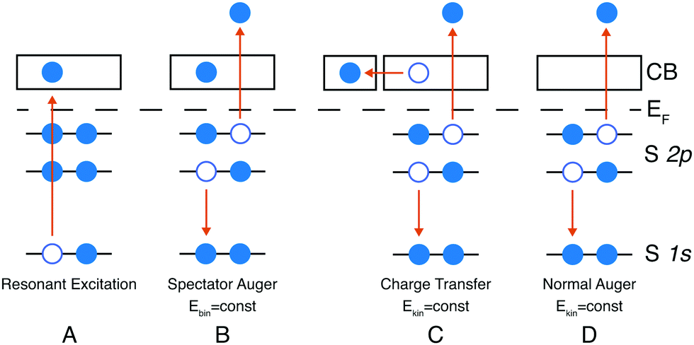 | ||
| Fig. 1 Spectator and charge transfer decay channels. | ||
Herein we only discuss the spectator channel of the radiation-less decay path of the core excited state with final states having two holes and one excited electron. If the excited electron itself participates in filling the core-hole, the final state contains only a single core-hole – a final state akin to that of direct core or valence ionisation. Such participator decays yield electrons with higher kinetic energies than those from the spectator channel considered here. For instance, the lowest kinetic energy participator would be that which leaves a hole in the 2s orbital, these electrons would have a kinetic energy of about 2.2 keV which is outside our considered kinetic energy region.
The dispersing and non-dispersing spectral features can be identified as shown in Fig. 2, where the dispersing (coherent) feature can be seen fitted in blue and the non-dispersing (non-coherent) in orange. The charge transfer time (τCT) can then be calculated from the ratio of the dispersing (In) and the non-dispersing (Ik) features, this is the so-called Raman ratio, multiplied with the core-hole lifetime (τ1s) as in eqn (1), where the core-hole lifetime is calculated from the lifetime broadening (Γ) of the S 1s core level far above the ionisation threshold through Heisenberg's uncertainty principle (τ1s = ħ/Γ). The lifetime broadening of the S 1s line is determined as the Lorentzian broadening of a fitted Voigt line-shape (see Fig. 4), the Gaussian broadening is the experimental broadening determined from a fitted Au 4f line with known lifetime broadening.26
 | (1) |
 | ||
| Fig. 2 Four S KLL spectra taken over the resonance showing the coherent and non-coherent contributions. | ||
The time-scales measured using core hole clock spectroscopy are different from that of pump–probe spectroscopy, as has been shown for the PCPDTBT:PCBM system.21 The difference arises from that while an optical excitation occurs between valence orbitals (or the valence band) to the unoccupied orbitals (conduction band) which are diffuse of delocalised in the system, an excitation with an X-ray is localised since the core hole is localised. The localisation makes core hole clock spectroscopy chemically specific and the resonant Auger pathways are very sensitive to the local energy landscape of the excited electron: for instance, the MoS2 monolayer/graphene system the charge transfer time have been measured to be 300 attoseconds have been found,16 whereas here we study multilayered and even bulk systems and reach charge transfer times below 100 attoseconds. The dynamics probed by optical excitations are as seen for instance in the MoS2 Ag nanoparticle system19 slower, i.e. between several femtoseconds to picoseconds.
Results
Fig. 3 shows scanning electron micrographs of the nano-crystalline and the rGO composite sample. There is a clear difference in the morphology of the samples, the nano-crystalline sample in Fig. 3a shows micrometer sized ball-like structure built up of MoS2 sheets several hundreds of nanometers long but only a few to tens of nanometers thick. This structure is not duplicated in the rGO composite (Fig. 3b and c) where the entire sample is a web of these long and very thin MoS2 sheets. This change in morphology is attributed to the graphene oxide in the rGO composite, which gives a backbone structure for the MoS2 sheets to grow on and to form this type of network structure. Whilst the nanoparticles instead form from a single nucleation site which then is the centre of these balls. | ||
| Fig. 3 (a–c) Shows scanning electron micrographs of the nanoparticles (a) and reduced graphene oxide laminates (b and c). (d) shows a TEM bright field image of MoS2–rGO composite sheets. (e) a High resolution image together with FFT (inset) showing the presence of several MoS2 lattice planes. | ||
The powder X-ray diffraction spectra (presented in Fig. S1, ESI†) of the rGO composite and the nano-crystals indicates crystalline MoS2 where the highest peak comes from the (002) plane distance. The peaks are relatively broad which is indicative of a small particle size. This is in agreement with the SEM micrographs and the thin MoS2 sheets. In the spectra of the rGO sample, there is also a small and broad peak at 23° which is attributed to graphene oxide.27
The Raman spectra of single crystal, nano-particle and rGO composite MoS2 (Fig. S1, ESI†) are similar with the two bands at around 400 cm−1 that are attributed to an in-plane Raman active mode, E12g, at 383 cm−1, and an out-of-plane mode, A1g, at 408 cm−1 of bulk MoS2.28 The splitting between these two bands is a fingerprint of the thickness of the MoS2, where the split of all these samples, 26 cm−1, corresponds to bulk (thicker than 5 layers) MoS2.29 For the rGO sample the two bands at 1350 cm−1 and 1600 cm−1 are from the graphene oxide, they are the D-band (from defects in the graphite plane) and the G-band (from in-plane vibrations).30
The transmission electron microscopy (TEM) images in Fig. 3d and e show the presence of MoS2 lamellae with a diameter in of typically 50–150 nm. The lamellae are disordered resulting in rings in the FFT of the high resolution image as well as in the diffraction pattern.
The sulphur 1s core level photoelectron spectra in Fig. 4 all show a single prominent peak, with varying width. The spectra have been fitted with a Voigt line-shape and a Shirley background. For each S 1s spectra the Gaussian contribution to the Voigt line profile (the experimental broadening) was determined from fitting of the well-known Au 4f7/2 line recorded with same beamline settings and with the know Lorentzian (lifetime) broadening of 0.3 eV.26 The Gaussian broadening was: 0.47 eV for the single crystal; 0.41 eV for the NP sample, and 0.42 eV for the rGO-composite sample.‡ Keeping the Gaussian contribution fixed at this value the Lorentzian FWHM changes between the different samples and the least squares fit reproduces the experimental line-shape well. However keeping the Lorentzian FWHM the same between the samples and changing the Gaussian FWHM does not reproduce the experimental line-shape. The core-hole lifetime is thereby different for the S 1s core-hole depending on the chemical surrounding. The calculated core-hole life-times can be seen in Table 1.
 | ||
| Fig. 4 S 1s core-levels spectra of the three samples. | ||
| Name |
τ
S![[thin space (1/6-em)]](https://www.rsc.org/images/entities/char_2009.gif) 1s [fs] 1s [fs] |
τ CT [as] | Raman ratio [.] |
|---|---|---|---|
| Single crystal | 1.450 | 63.8 | 0.044 |
| Nanoparticles | 0.954 | 45.8 | 0.048 |
| In rGO | 0.856 | 38.2 | 0.045 |
The Mo 3p (Fig. S2, ESI†) and S 1s (Fig. 1) spectra of all the samples consists of single species, indicative of pure MoS2 in all of them. The binding energy position of the core-levels change between the different samples. Comparing the SC and the NP samples there is a shift of the same magnitude in both Mo 3p and S 1s towards lower binding energies, which is consistent with a change of work-function. The introduction of the rGO yields additional changes, in this case there is a larger change to higher binding energy of the Mo 3p line compared to the S 1s. This difference can either be due to a different chemical shift of both core-levels or a change in work-function combined with a chemical shift of one or both of the core-levels. This is discussed in detail below. The spectra of the rGO sample also have a large C 1s (Fig. S3, ESI†) and O 1s (Fig. S4, ESI†) contribution which is consistent with the presence of graphene oxide.
In the left part of Fig. 5 total fluorescence yield X-ray absorption spectra of the different samples can be seen. The onset of the absorption peak is the same for all the samples but the first feature of the resonance is slightly narrower for the nanoparticles and the nanoparticle–rGO samples. The excitation geometry is in grazing incidence with respect to the photon beam. The linear polarisation is in the horizontal plane of the beam and perpendicular to it, so perpendicular to the sample surface. Hence parallel to the c-axis in the case of single crystal MoS2 this means that the S 3pz orbital will be preferentially populated, for the other two samples a mixture of 3px,y,z will be populated. This result is in concurrence with other XAS studies on MoS2.15
 | ||
| Fig. 5 X-ray absorption (left), resonant Auger (middle) and calculated charge transfer times (right) for single crystals, nanoparticles and laminates with rGO. | ||
Over the entire S K-edge resonance, electron spectra in the S KL2,3L2,3 kinetic energy region are recorded while stepping the photon energy. The photon energies of interest are identified from the X-ray absorption recorded in the vicinity of the S K-edge absorption edge as seen in the left panels of Fig. 5. Each of these Auger spectra are then stacked to form the resonant Auger spectroscopy 2D-maps seen in the middle panel of Fig. 5. Individual spectra in this 2D-map are then chosen and fitted using a least squares fit procedure (described in the ESI†) to identify and quantify the coherent and non-coherent contributions. Examples of these fits are shown in Fig. 2. From the fits the charge transfer times are then calculated using eqn (1), the calculated charge transfer times can be seen in Fig. 5 and 6. The error from the fitting procedure is in the percent range and fits within the size of the markers.
 | ||
| Fig. 6 Comparison of the Raman ratios (top) and the corresponding charge transfer times (bottom) for the different samples. The two coloured lines highlights the two different regions of the charge transfer in the MoS2 reduced graphene oxide sample showing the effect of the Schottky barrier. | ||
The resonant Auger 2D-map for the three samples are presented in the middle column of Fig. 5. All three spectra exhibit the same spectral features, a coherent channel at 2115 eV and a dispersing in-coherent channel, from the 1D2 Auger final state. At 2107 eV there are weaker decay channels that also are visible, they exhibit the same shape and form as the main feature and are decays with the final state 1S0. Fitting the spectra and calculating the charge transfer time using eqn (1) yields the charge transfer times plotted in the right column of Fig. 5. The charge transfer times follow the same trend in all three samples, on-top of the resonance the charge transfer is slower but when de-tuning over the resonance it becomes faster up to a certain point where it reaches a steady state. In this stable region, at photon energies around 2474 eV, the charge transfer times are the shortest.
In Fig. 6 the calculated Raman ratios and the corresponding charge transfer times are presented for comparison, while the shortest charge transfer time and corresponding Raman ratio for each sample is presented in Table 1. The Raman-ratio is very similar between the single crystal and the nanoparticle samples and at higher excitation energy between all three samples. Close to the resonance the MoS2–rGO composite shows a different behaviour than the other two samples, this is manifested as two regions (guide for the eye in yellow and purple).
Looking at the region of the fastest charge transfer times (2474 eV and above) a trend is noticeable between the different samples, charge transfer is fastest in the nanoparticle–rGO composite–rGO composite and slowest in the single crystal. The charge transfer time is decreased from 64 to 38 attoseconds when creating nanoparticles and locking them onto a graphene oxide backbone network. The difference in charge transfer time arise from the difference in lifetimes of the core-excited state.
The result of the single crystal sample can be compared to the recent study by Woicik et al.15 where resonant Auger spectroscopy was performed on bulk single crystal MoS2. However, they did not calculate any charge transfer time within their work. Fitting of their published spectra (interpolated from their published figure with a significant error bar) and calculating the charge transfer time using the same core-hole lifetime as our experiment yields a shortest charge transfer time of 51 attoseconds when de-tuning over the resonance, similar to our results.
In the region around 2473 eV there is a noticeable difference between the pure MoS2 samples (the single crystal and the nanoparticle samples) and the MoS2 with the graphene oxide backbone. The charge transfer time for the two pure MoS2 samples shows a similar exponential decay behaviour while de-tuning, which is expected, while the rGO sample has a kink in this just below 2473 eV but otherwise also follows the same exponential behaviour. This could also be regarded as two regions both with exponential decays, this is discussed in detail below.
Discussion
Despite the very different appearance of the three MoS2 samples in this study, their electronic structure is very similar. The core-level XPS show pure MoS2 characteristics in all three with the difference that the life-time of the core-hole is shorter when the MoS2 particles are small and in contact with graphene oxide. This can be explained with an increase in the number of available decay channels i.e. increase in the density of states.21 Comparing the life-times of the S 1s two things stands out. The two samples with nano-sized flakes (NP and rGO) exhibit a shorter core-hole life-time than the single crystal. This can be explained through heavier n-doping from the smaller crystal flakes. The n-doping of bulk MoS2 is caused by sulphur defects leaving unpaired molybdenum valence electrons. The edges of a MoS2 flake are also prone to metallic edge-states increasing the n-type doping close to the edges.31 With the increasing edge to bulk ratio in the NP and rGO the doping level will be much higher than in the SC. The n-type doping will introduce a dopant level in the band-gap of the MoS2 close to the conduction band thereby introducing more decay paths but in the same electronic state i.e. higher density of states but no new matrix elements which will lead to a decrease in the lifetime of the excited state.There is also a difference in the S 1s lifetime of the rGO and the NP samples. This is promoted by the increase of density of states in the interface between the graphene sheet and the MoS2. In this interface there will be a depletion of electrons in the graphene and a corresponding accumulation on the sulphur closest to the interface in the MoS2.16 This can be viewed as either the formation of a Schottky barrier or a interfacial dipole as discussed more below.32 Garcia-Basabe et al. observed a charge transfer time that was almost halved in the heterostructure of monolayer MoS2 and graphene versus a pure monolayer, while we observe a 40% drop. In the rGO sample the MoS2 is bulk-like (more than 5 monolayers thick) on-top of the graphene sheet meaning that we do not have the same interfacial area as the monolayer MoS2 to graphene, leading to a mix of the behaviour of the small flake doping and the charge depletion from the graphene. With a controlled growth of the rGO composite terminating at monolayer thickness the charge transfer could potentially be even faster.
All three samples follow the previously reported exponential decrease in the charge transfer time in 2D-crystal materials while de-tuning over the resonance33 with the exception of the rGO sample, where two stable regions can be seen. The first just before 2473 eV excitation energy and the second coincides with the stable region of the other two samples. This first stable region can be explained by the formation of a Schottky barrier between the MoS2 and the rGO. Up to 2473 eV the charge transfer in all three samples is similar and can be explained by charge transfer within the MoS2. The interface between the MoS2 and the rGO creates a Schottky barrier with charge accumulation which will limit the charge transfer up to a certain excitation energy. This stable region extends for approximately 0.5 eV which is close to the height of the Schottky barrier between MoS2 and graphene (0.6–0.65 eV for MoS2/graphene34,35 and 0.6 for eV MoS2/graphite31). When increasing the excitation energy above the barrier height the charge transfer times drops quickly and can again be modelled with an exponential decay. The formation of a Schottky barrier or interfacial dipole also explains the core-level shifts in the Mo 3p and S 1s core-levels between the NP and rGO sample. The shift consists of two contribution, first, a change in the work function of the system which yields the same shift in both Mo 3p and S 1s and, second, a shift of the Mo 3p line to higher binding energy or a shift of the S 1s to lower binding energy. The second shift is a chemical shift that is either from decreased electron density on the Mo sites or increased electron density on the S sites. The latter case is consistent with the formation of a interfacial dipole at the interface between the outermost sulphur atoms and the rGO sheet.
This Schottky barrier behaviour is also evidence for well reduced graphene oxide, meaning that the graphene oxide has similar properties to pure graphene. This is evident since the Schottky barrier is of n-type and in the order of 0.5 eV, a pure graphene oxide/MoS2 interface would yield a p-type Schottky barrier of around 1 eV. This can also be collaborated with the C 1s XPS spectra, as can be seen in Fig. S3 (ESI†) of the rGO sample with a narrow component attributed to sp2 carbon and with a small shoulder on the high binding energy side from sp3 carbon, either C–C or C–H and a small C–O contribution, this is similar to the spectra of graphene.36,37
The charge transfer times measured herein fall outside the range of 0.1 to 10 times the core hole's lifetime that is given by Wurth and Menzel.38 A direct comparison between an analysis of the S KLL (resonantly excited around the S K-edge) and S LMM (excited around the L1-edge) is available for the S/Ru(0001) system.39 In ref. 38 the limit of 10% of the core-hole lifetime is given by the what fraction between the spectral areas “…which can be determined experimentally with reasonable accuracy…”. The case of Ar LMM and S LMM spectra as investigated in e.g.ref. 38 and 39 a fraction of 10% is what is determinable. However In Fig. 2 the least squares fit of the S KLL spectra are exhibited, our analysis is based on the areas of the dispersing and non-dispersing signatures (see 2D-maps in Fig. 5) where we can track the relative intensity of the dispersing feature farther before it disappears in the noise of the background. In a study on black phosphorous a wider range of charge transfer times have been shown to be accessible since the contrast in the resonant auger spectra in the KLL region is high,40 also as mentioned above performing this analysis on data for MoS2 from ref. 15 we arrive at similar charge transfer times.
Conclusions
In conclusion we show that the charge transfer time, as inferred from the core-hole clock technique depends on the chemical surrounding and the morphology of the system. Breaking the symmetry of the crystal we obtain swifter charge transfer times – up to 40% faster in the nanocomposite compared to a bulk single crystal. Using tunable X-rays in the region where core excitation from a 1s level is possible and recording the resonant Auger spectra in the KLL region gives – at least for row III elements – enough contrast to allow the determination of charge transfer times in the tens of attoseconds regime. Core-hole clock spectroscopy with hard X-rays is a general method to study these timescales.We also show that the signature of a Schottky barrier can be seen in the nanocomposite case with two distinct regions in the charge transfer time both exhibiting the signature exponential drop of resonant Raman channel. This is evidence that ultra-fast charge transfer in molybdenum disulphide can be tailored which should be taken into account in the design of emergent devices.
Conflicts of interest
There are no conflicts to declare.Acknowledgements
A. L. acknowledges the support from the Swedish Research Council (grants no. 2014-6463 and 2018-05336) and Marie Sklodowska Curie Actions (Cofund, Project INCA 600398). F. J. acknowledges financial support from the K G Westman foundation. We thank HZB for the allocation of synchrotron radiation beamtime and Roberto Felix Duarte for assistance at the KMC-1 beamline.References
- K. Novoselov, A. Mishchenko, A. Carvalho and A. C. Neto, Science, 2016, 353, aac9439 CrossRef CAS PubMed.
- G. R. Bhimanapati, Z. Lin, V. Meunier, Y. Jung, J. Cha, S. Das, D. Xiao, Y. Son, M. S. Strano, V. R. Cooper, L. Liang, S. G. Louie, E. Ringe, W. Zhou, S. S. Kim, R. R. Naik, B. G. Sumpter, H. Terrones, F. Xia, Y. Wang, J. Zhu, D. Akinwande, N. Alem, J. A. Schuller, R. E. Schaak, M. Terrones and J. A. Robinson, ACS Nano, 2015, 9, 11509–11539 CrossRef CAS PubMed.
- Q. H. Wang, K. Kalantar-Zadeh, A. Kis, J. N. Coleman and M. S. Strano, Nat. Nanotechnol., 2012, 7, 699 EP CrossRef PubMed.
- J. Hong, Z. Hu, M. Probert, K. Li, D. Lv, X. Yang, L. Gu, N. Mao, Q. Feng, L. Xie, J. Zhang, D. Wu, Z. Zhang, C. Jin, W. Ji, X. Zhang, J. Yuan and Z. Zhang, Nat. Commun., 2015, 6, 6293 EP CrossRef PubMed.
- M.-L. Tsai, S.-H. Su, J.-K. Chang, D.-S. Tsai, C.-H. Chen, C.-I. Wu, L.-J. Li, L.-J. Chen and J.-H. He, ACS Nano, 2014, 8, 8317–8322 CrossRef CAS PubMed.
- B. Radisavljevic, A. Radenovic, J. Brivio, V. Giacometti and A. Kis, Nat. Nanotechnol., 2011, 6, 147 CrossRef CAS PubMed.
- R. Ganatra and Q. Zhang, ACS Nano, 2014, 8, 4074–4099 CrossRef CAS PubMed.
- J.-M. Yun, Y.-J. Noh, J.-S. Yeo, Y.-J. Go, S.-I. Na, H.-G. Jeong, J. Kim, S. Lee, S.-S. Kim, H. Y. Koo, T.-W. Kim and D.-Y. Kim, J. Mater. Chem. C, 2013, 1, 3777–3783 RSC.
- X. Gu, W. Cui, H. Li, Z. Wu, Z. Zeng, S.-T. Lee, H. Zhang and B. Sun, Adv. Energy Mater., 2013, 3, 1262–1268 CrossRef CAS.
- A. C. Domask, R. L. Gurunathan and S. E. Mohney, J. Electron. Mater., 2015, 44, 4065–4079 CrossRef CAS.
- Q. Sun, H. Miao, X. Hu, G. Zhang, D. Zhang, E. Liu, Y. Hao, X. Liu and J. Fan, J. Mater. Sci.: Mater. Electron., 2016, 27, 4665–4671 CrossRef CAS.
- Y. Li, H. Wang, L. Xie, Y. Liang, G. Hong and H. Dai, J. Am. Chem. Soc., 2011, 133, 7296–7299 CrossRef CAS PubMed.
- K. Chang and W. Chen, ACS Nano, 2011, 5, 4720–4728 CrossRef CAS PubMed.
- E. G. da Silveira Firmiano, A. C. Rabelo, C. J. Dalmaschio, A. N. Pinheiro, E. C. Pereira, W. H. Schreiner and E. R. Leite, Adv. Energy Mater., 2014, 4, 1301380 CrossRef.
- J. C. Woicik, C. Weiland, A. Rumaiz, M. Brumbach, N. Quackenbush, J. Ablett and E. Shirley, Phys. Rev. B, 2018, 98, 115149 CrossRef CAS.
- Y. Garcia-Basabe, A. R. Rocha, F. C. Vicentin, C. E. Villegas, R. Nascimento, E. C. Romani, E. C. De Oliveira, G. J. Fechine, S. Li and G. Eda, et al. , Phys. Chem. Chem. Phys., 2017, 19, 29954–29962 RSC.
- U. Aygül, H. Peisert, D. Batchelor, U. Dettinger, M. Ivanovic, A. Tournebize, S. Mangold, M. Förster, I. Dumsch and S. Kowalski, et al. , Sol. Energy Mater. Sol. Cells, 2014, 128, 119–125 CrossRef.
- U. B. Cappel, S. Plogmaker, J. A. Terschlüsen, T. Leitner, E. M. Johansson, T. Edvinsson, A. Sandell, O. Karis, H. Siegbahn and S. Svensson, et al. , Phys. Chem. Chem. Phys., 2016, 18, 21921–21929 RSC.
- W. Lin, Y. Shi, X. Yang, J. Li, E. Cao, X. Xu, T. Pullerits, W. Liang and M. Sun, Mater. Today Phys., 2017, 3, 33–40 CrossRef.
- P. Brühwiler, O. Karis and N. Mårtensson, Rev. Mod. Phys., 2002, 74, 703 CrossRef.
- F. O. Johansson, M. Ivanovic, S. Svanström, U. B. Cappel, H. Peisert, T. Chassé and A. Lindblad, J. Phys. Chem. C, 2018, 122, 12605–12614 CrossRef CAS.
- B. Borges, L. Roman and M. Rocco, Top. Catal., 2019, 1–7 Search PubMed.
- Q. Xiang, J. Yu and M. Jaroniec, J. Am. Chem. Soc., 2012, 134, 6575–6578 CrossRef CAS PubMed.
- F. Schaefers, M. Mertin and M. Gorgoi, Rev. Sci. Instrum., 2007, 78, 123102 CrossRef CAS PubMed.
- M. Gorgoi, S. Svensson, F. Schäfers, G. Öhrwall, M. Mertin, P. Bressler, O. Karis, H. Siegbahn, A. Sandell and H. Rensmo, et al. , Nucl. Instrum. Methods Phys. Res., Sect. A, 2009, 601, 48–53 CrossRef CAS.
- M. Patanen, S. Aksela, S. Urpelainen, T. Kantia, S. Heinäsmäki and H. Aksela, J. Electron Spectrosc. Relat. Phenom., 2011, 183, 59–63 CrossRef CAS.
- K. Zhang, Y. Zhang and S. Wang, Sci. Rep., 2013, 3, 3448 CrossRef PubMed.
- K.-G. Zhou, F. Withers, Y. Cao, S. Hu, G. Yu and C. Casiraghi, ACS Nano, 2014, 8, 9914–9924 CrossRef CAS PubMed.
- C. Lee, H. Yan, L. E. Brus, T. F. Heinz, J. Hone and S. Ryu, ACS Nano, 2010, 4, 2695–2700 CrossRef CAS PubMed.
- P. Ahlberg, F. Johansson, Z.-B. Zhang, U. Jansson, S.-L. Zhang, A. Lindblad and T. Nyberg, APL Mater., 2016, 4, 046104 CrossRef.
- C. Zhang, A. Johnson, C.-L. Hsu, L.-J. Li and C.-K. Shih, Nano Lett., 2014, 14, 2443–2447 CrossRef CAS PubMed.
- S. Braun, W. R. Salaneck and M. Fahlman, Adv. Mater., 2009, 21, 1450–1472 CrossRef CAS.
- F. Johansson, Y. Sassa, T. Edvinsson and A. Lindblad, 2019, ARXIV.
- A. Chanana and S. Mahapatra, J. Appl. Phys., 2016, 119, 014303 CrossRef.
- C. Jin, F. A. Rasmussen and K. S. Thygesen, J. Phys. Chem. C, 2015, 119, 19928–19933 CrossRef CAS.
- M. J. Webb, P. Palmgren, P. Pal, O. Karis and H. Grennberg, Carbon, 2011, 49, 3242–3249 CrossRef CAS.
- Y.-E. Shin, Y. J. Sa, S. Park, J. Lee, K.-H. Shin, S. H. Joo and H. Ko, Nanoscale, 2014, 6, 9734–9741 RSC.
- W. Wurth and D. Menzel, Chem. Phys., 2000, 251, 141–149 CrossRef CAS.
- A. Föhlisch, S. Vijayalakshmi, F. Hennies, W. Wurth, V. Medicherla and W. Drube, Chem. Phys. Lett., 2007, 434, 214–217 CrossRef.
- F. O. Johansson, Y. Sassa, T. Edvinsson and A. Lindblad, 2020, arXiv preprint arXiv:2003.13394.
Footnotes |
| † Electronic supplementary information (ESI) available: Sample characterisation by XPS, XRD and Raman spectroscopy. See DOI: 10.1039/d0cp00857e |
| ‡ The measurements of the three different samples were made over a period of two years where changing beamline conditions gives different experimental broadening for the different samples. |
| This journal is © the Owner Societies 2020 |