
 Open Access Article
 This Open Access Article is licensed under a
 Creative Commons Attribution 3.0 Unported Licence
Engineering work function of graphene oxide from p to n type using a low power atmospheric pressure plasma jet†
Avishek
Dey
 a,
Paheli
Ghosh
a,
James
Bowen
a,
Nicholas St. J.
Braithwaite
b and
Satheesh
Krishnamurthy
*a
a,
Paheli
Ghosh
a,
James
Bowen
a,
Nicholas St. J.
Braithwaite
b and
Satheesh
Krishnamurthy
*a
aSchool of Engineering and Innovation, The Open University, Milton Keynes, MK7 6AA, UK. E-mail: Satheesh.Krishnamurty@open.ac.uk
bSchool of Physical Sciences, The Open University, Milton Keynes, MK7 6AA, UK
First published on 23rd January 2020
Abstract
In this work, we demonstrate doping graphene oxide (GO) films using a low power atmospheric pressure plasma jet (APPJ) with subsequent tuning of the work function. The surface potential of the plasma functionalized GO films could be tuned by 120 ± 10 mV by varying plasma parameters. X-ray spectroscopy used to probe these changes in electronic structure of systematically functionalized GO films by plasma. Detailed investigation using X-ray photoelectron spectroscopy and near edge X-ray absorption fine structure spectroscopy revealed the reactive nitrogen species in the plasma induce finite changes in the surface chemistry of the GO films, introducing additional density of states near the top of the valence band edge. Nitrogen introduced by the atmospheric pressure plasma is predominantly in a graphitic configuration with a varying concentration of pyridinic nitrogen. Additionally, evidence of gradual de-epoxidation of these GO films with increasing plasma exposure was also observed. We attribute this variation in work function values to the configuration of nitrogen in the graphitic structure as revealed by X-ray spectroscopy. With pyridinic nitrogen the electronic states of GO became electron deficient, inducing a p-type doping whereas an increase in graphitic nitrogen increased the electron density of GO leading to an n-type doping effect. Nitrogen doping was also found to decrease the resistivity from 138 MΩ sq−1 to 4 MΩ sq−1. These findings are extremely useful in fabricating heterojunction devices like sensors and optoelectronic devices where band structure alignment is key to device performance when GO is used as a charge transport layer. This technique can be extended to other known 2D systems.
1. Introduction
Graphene, since its discovery in 2004 has attracted enormous interest due to its physical and chemical properties, and wide applications.1 Graphene oxide (GO) has emerged as an attractive alternative to graphene due to low cost, large scale production and solution processability. GO is prepared by oxidative exfoliation of graphite.2 Due to the presence of polar oxygen functional groups GO is highly hydrophilic and is easily dispersible in water, as well as many organic solvents. These oxygen-containing functional groups play a crucial role in defining its optical and electronic properties.3 The basal plane of GO is decorated with hydroxyl and epoxy functional groups while carboxyl, carbonyl and phenol groups are attached to the edges of the graphene sheet.3 The work function is a fundamental electronic property of a material and can be used to interpret the relative position of the Fermi level.4 The work function is defined as the energy required to remove an electron from the highest occupied level in the Fermi distribution of a solid to vacuum. For efficient transport of electrons or holes in a heterojunction device, the work function of the materials play a crucial, since work function determines how the bands will align at the contacts.Recently there has been an increased interest in applications of GO for interfacial layers5,6 and transparent electrode materials in optoelectronic devices7,8e.g. liquid crystal displays (LCDs), organic light emitting diodes (OLEDs), touch screens, dye-sensitized solar cells (DSSCs) and as supercapacitor electrodes.9 Tuning the work function of GO is key to achieving high performance devices. The most common methods to tune the work function of GO are by reduction via thermal, chemical and electrochemical processes.10 Molecular dynamics and density functional theory calculations by Kumar et al.11 provided a detailed insight into the impact of various oxygen functional groups on the work function of reduced graphene oxide (rGO). According to them, the work function of rGO can be tuned up to ∼2.5 eV by varying the composition of oxygen-containing functional groups. Sygellou et al.12 studied the variation in work function of GO via three different reduction processes. They found the work function decreases by ∼1 eV between GO and reduced GO. Other approaches to tailor the work function of GO include Au-ion incorporation,13 UV irradiation14 and exposure to soft X-rays.15 In the case of p-channel in organic field-effect transistors (OFETs)16 efficient injection of holes is achieved by matching the work function of electrodes with the highest occupied molecular orbital (HOMO) level of the organic semiconductor. For LEDs efficient electron injection is achieved by matching the work function with lowest unoccupied molecular orbital (LUMO) of the active layer. The ability to tune the work function makes GO a suitable candidate for use as charge injection layers for both as electron and hole transport layers.5
Doping GO with nitrogen has been a widely used strategy to improve its properties, for example as a catalyst for oxygen reduction reactions, in biosensors, in ultracapacitors, and as electrodes in lithium ion batteries.17 Due to its comparable atomic radius and five valence electrons, nitrogen is considered as the ideal element for substituting carbon atoms in GO. A recent review by Dey et al. focuses on the advantages of plasma over other functionalisation techniques. Out of the various techniques used so far, functionalising with plasma is the most promising one as plasma processing does not involve chemical precursors and by-products.18 Atmospheric pressure plasma jets (APPJs) deliver charged particles, neutral metastable species, radicals and radiation in the UV and visible regions conveniently in a processing plume.19 Liu et al. treated graphene counter-electrodes, made via screen printing process with atmospheric pressure plasma operated at 700 W. They found that by introducing these plasma treated reduced graphene oxide (rGO) as counter electrodes, DSSCs showed power conversion efficiencies of 5.19% comparable to those of furnace-calcined counter electrode while requiring a much shorter process time.20 Alotaibi et al. used atmospheric air plasma operated at a high power (300 W, 20 kHz) and a high potential of ∼10 kV to reduce graphene oxide to conductive graphene films.21 All these processes are not a low temperature process as the plasma is an arc discharge. Other attempts include APPJ treatment of graphene to increase hydrophilicity22 and introduction of bandgap at an input power of 150 W.23 In this study it will be shown that a APPJ can be used as tool for controlled doping graphene oxide. Kelvin probe force microscopy (KPFM) was used to depict any changes in electronic properties of these plasma functionalised GO films. And to understand the changes in electronic properties with element specificity, these plasma functionalised GO films were investigated using X-ray photoelectron spectroscopy (XPS) and near-edge X-ray absorption fine structure spectroscopy (NEXAFS).
APPJ is non-equilibrium in nature and is operated at 4 W, which is lowest input power reported till date. Here the low power associated with the plasma source provides a significant advantage over other plasma-based techniques reported so far. Additionally, the degree of damage to the GO films following the plasma treatment is negligible as seen form atomic force microscopy and scanning electron microscopy. This allows GO films to be functionalised directly on flexible and polymeric substrates. Major advantage of this technique is the ability to perform surface chemical and electronic modifications in a controlled manner at low temperature and atmospheric pressure with minimal power consumption. This opens future pathways for roll-to-roll processing of GO films for large-scale, flexible electronics applications.
2. Experimental details
Synthesis of GO
The GO was prepared from natural graphite flakes following a modified Hummers’ method,24 which involves the oxidative exfoliation of graphite. During reaction, the strong oxidative species intercalate between the graphite layers, increasing the interlayer spacing (from 0.34 nm to ∼1.08 nm). The loosely bound layers are then delaminated using ultrasonication to extract GO. To produce films, 10 mg of GO was ultra-sonicated in 100 mL of distilled water for one hour. This solution was centrifuged at 8000 rpm for 10 min and the supernatant was drop cast onto a silicon substrate of approximate dimensions 5 mm × 5 mm. The substrates were then heated at 80 °C in an oven to remove excess water.Functionalization of GO
Plasma treatment of the synthesised GO was the final step. Experimental setup to carry out the functionalization process is presented in Fig. 1. A gas mixture of helium and nitrogen was used to ignite the plasma. The design and operating principle of the plasma jet is described below. GO films were kept at a minimum distance of 5 mm from the substrates to avoid arcing between the sample and electrodes. Flow rates were optimised to achieve the least input power, 4 W in this case. The GO films were then exposed to APPJ for 5 s, 10 s, 20 s, 30 s, 1 min, 2 min and 3 min. This process yielded 8 types of specimen including the untreated material.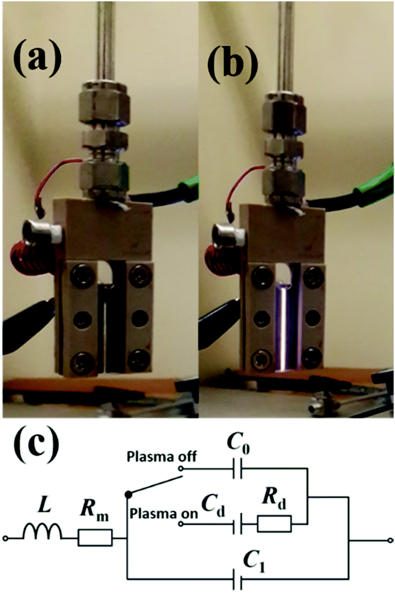 | ||
| Fig. 1 RF-microplasma jet used for the functionalisation of GO with (a) plasma on and (b) plasma off conditions. Equivalent electrical circuit (c) of the device. | ||
Characterization
Scanning Kelvin probe microscopy (SKPM) also known as Kelvin probe force microscopy (KPFM) measurements were carried out to realize changes in work function of the GO films with plasma functionalization. The measurements were performed using an Asylum Research MFP-3D atomic force microscope. Surface potential measurements were performed with Pt–Ir coated silicon probes (PPP-EFM, Nanosensors) with nominal force constant of 2.8 N m−1. The tip was biased at +3 V with a drive amplitude of 300 mV. The image parameters were set at scan size of 10 μm × 10 μm, scan rate 1 Hz, 512 × 512 pixels. In SKPM the instrument detects the surface potential (SP) as the work function difference between the tip and the sample surface, i.e. SP = ΦTip − ΦSample. To calibrate the work function of the Pt–Ir tip, sputter cleaned polycrystalline silver was used. For silver the SP was measured to be 0.29 mV. Considering for polycrystalline silver ΦSilver = 4.26 eV, ΦTip was calculated to be ∼4.55 eV.To understand the changes in electronic and chemical structure of the GO films upon plasma functionalization, X-ray spectroscopies (XPS and NEXAFS) were carried out at beamline 8-2 at the Stanford Synchrotron Radiation Lightsource (SSRL).25 The incoming flux (I0) was measured using a gold grid placed in the beam path upstream of the chamber and was used to normalize the spectra to avoid any artefact due to beam instability and monochromator absorption features. All samples were mounted on an aluminium stick using a conductive carbon tape and transferred to the main chamber via load lock, both chambers were under an ultra-high vacuum of <1 × 10⁻⁸ Torr (<1.33 × 10⁻⁶ Pa).
NEXAFS spectroscopy is a powerful element-specific tool to probe the local geometric and electronic structure of carbon related materials. NEXAFS spectra correspond to transitions from core level to unoccupied or partially occupied DOS in the electronic structure and provides a unique fingerprint of local structure. For nitrogen-functionalized graphene structures where deconvolution of XPS features is ambiguous, NEXAFS becomes effective in distinguishing between different bonding configurations.26 Carbon and oxygen K-edge NEXAFS spectra showing 1s–π* and 1s–σ* transitions were acquired in total electron yield (TEY) mode for GO and functionalized GO samples. To interpret the NEXAFS data, first a linear background was subtracted from the region before the carbon absorption edge. The subtracted spectra were normalized in the post-continuum region to have ‘one unit' in the background signal at 330 eV, following the protocols of Banerjee et al.26 C K-edge spectra were calibrated to the exciton feature of HOPG at 291.65 eV and O K-edge spectra were calibrated to oxide dip from the gold mesh (531.2 eV) respectively. XPS data analysis was performed with CasaXPS software using a Shirley background subtraction.27 Preferably to give equal weightage to instrumental broadening (Gaussian) and intrinsic lifetime broadening of the core holes (Lorentzian). A combination of Gaussian (50%) and Lorentzian (50%) line shape functions were used to fit the core level spectra except HOPG. The sheet resistance of plasma-functionalized graphene oxide films was measured using a Jandel RM3000+ four-point probe.
3. Results and discussions
The atmospheric pressure plasma jet used for functionalization of graphene oxide films is shown in Fig. 1. Plasma is ignited by applying radio frequency (RF) power between two stainless steel electrodes through a series LC circuit. The LC circuit is chosen to have a resonance frequency of 13.56 MHz. In this case the circuit consists of a tuneable capacitor (Cext = 2–22 pF) and an inductor (L = 16.5 μH, Micrometals T68-6 core).28 When the applied RF frequency matches to that of the LC circuit, the voltage drop across the electrodes gets amplified, a resonance effect, to initiate the discharge. At resonance, the voltage across the electrodes has been found to be 100 times that of the input voltage. But with an active discharge between the electrodes, this value drops by a factor of 2 due to the power dissipated in the discharge. In actual practice when the plasma is on, the discharge gap also needs to be considered and is to be added to the series LC circuit as shown in Fig. 1(c). To account for any shift in the resonance frequency, the drive frequency of the signal generator is tuned accordingly to achieve the desired resonance.With helium flowing between the electrodes at 2000 standard cubic centimetres per second (sccm), discharge could be generated for a power as low as 1 W. However, when nitrogen (1% of helium) is added to the system, the minimum power increases to 4 W to sustain the discharge. This power is significantly less than previously reported plasma jet sources for nanomaterial functionalization.18 The micro atmospheric pressure plasma jet (μAPPJ) used for functionalization has been developed by Marinov et al.28 The plasma of helium and nitrogen gas mixture was generated at a constant RF value of 13.56 MHz. The μAPPJ was based on a series LC resonance with the discharge gap being a part of the resonant circuit. With an applied RF power, the voltage across the discharge gap is amplified at resonance, enabling the ignition of the plasma. A power of 4 W was used to ignite the admixture of helium and nitrogen. Helium and nitrogen were kept at a constant flow rate of 2000 and 16 sccm respectively throughout the functionalization process using mass flow controllers. In this section, optical emission spectroscopy of the plasma is presented. The nature of the plasma depends on the gas phase composition, i.e. the excited atoms, ions and molecules. Fig. 2 presents the optical emission spectra (OES) of the plasma. The emission spectra reveal a variety of nitrogen emission peaks within the wavelength range of 200 nm to 880 nm. In the UV region, Fig. 2(a), several lines are observed between 316 nm to 406 nm corresponding to the second positive (C3Πu → B3Πg) molecular series of neutral N2 molecules. Additional peak at peaks at 391 nm and 427 nm correspond to the first-negative transitions of N2+ molecular ions. There also exist strong peaks in the region of 215 nm to 271 nm originating from the NO(γ) system (A2Σ+ → X2Π), representative of the presence of oxygen in the afterglow. Since the plasma is not just confined within the electrode for APPJ, so oxygen incorporation is highly likely. A prominent line at 308 nm corresponding to hydroxide (OH) emission is visible in the spectrum, which is attributed to the impurities in the gas supply. The visible region is dominated by the first positive molecular series of nitrogen (B3Πg → A3Σ+).29,30 The helium line at 706 nm, Fig. 2(b), in the nitrogen-enriched helium flow is strongly suppressed with respect to pure helium plasma. This is mainly due to the “quenching” of excited helium atoms on collision with nitrogen molecules resulting in excited nitrogen species in the plasma.31 As a result, nitrogen becomes the dominant species. The following equation presents the interaction between the helium atoms and molecules with the nitrogen molecules:
| He* + He* → He + He+ + e− |
| He*(n = 3) + He → He2+ + e− |
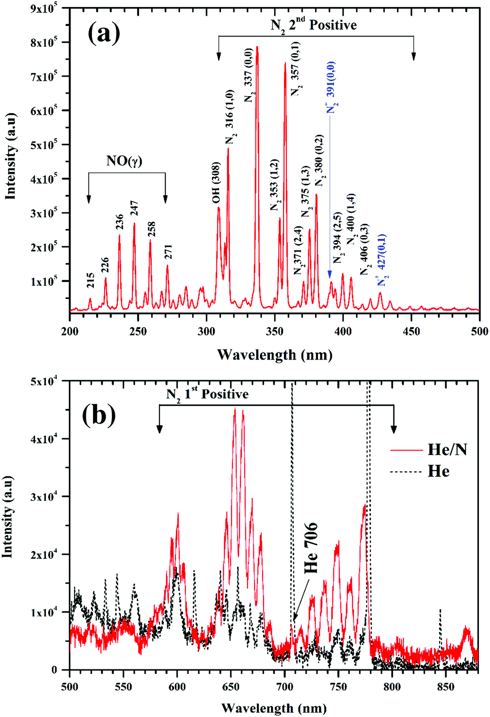 | ||
| Fig. 2 Optical emission spectra of He + N2 plasma, (a) in UV region (b) in visible region. The spectra shows the abundant presence of a range of nitrogen species in the plasma. | ||
After N2 addition:
| He* + N2 → He + N2+ + e− |
| He2(3Σu+) + N2 → He + He + N2+ + e− |
| He2+ + N2 → He + He + N2+ |
| He+ + 3N2 → He + 2N + 2N2+ + 0.3 eV |
XPS is a surface analysis technique and has been used here to gain insight into the changes in atomic concentration, local chemical environment, and co-ordination geometry of the GO thin films with plasma functionalization. By careful analysis of the core level spectra (C1s, O1s, N1s) it will be possible to understand the mechanism behind the changes in chemical environment. For nitrogen doped into graphitic lattice, there are multiple possible bonding configurations. Each of these bonding configurations effect the electronic structure of GO differently. The three most common configurations as shown in Fig. S1 (ESI†) are graphitic, pyridinic and pyrrolic nitrogen.17 Graphitic N, also referred to as quaternary N, is placed in the hexagonal lattice with three carbon neighbours. The two-fold coordinated state is called pyridinic N, whereas the nitrogen bonded into the five-membered heterocyclic ring is known as pyrrolic N. Of these bonding types, graphitic and pyridinic N are sp2 hybridized and pyrrolic N is sp3 hybridized. In addition to these, N oxides of pyridinic N have also been reported.32 Pyridine N donates one p electron to the aromatic π system while pyrrolic N contributes two electrons. Pyridinic N is highly reactive and is stable only under high vacuum conditions. Pyridinic N has not been of much interest as it fails in enhancing the properties of GO.33 Graphitic N is the most effective for promoting the applications of N-doped GO in oxygen reduction reactions (ORR),32 sensor,34 water oxidation35 and electromagnetic devices.36 On the other hand Pyrrolic N have been found to significantly enhance the Li storage capability,37 as the binding energy of the Li ion to pyrrole nitrogen is higher (1.3 eV) compared with quaternary nitrogen sites (0.95 eV). Though these bonding environments cannot be resolved directly in the carbon spectra, but can be extracted by deconvolving the nitrogen spectra revealing individual contributions (within ±0.1 eV of binding energy). The core level photoelectron spectra for carbon and oxygen is presented in Fig. 3. Spectra from individual functionalized states are overlaid to discern the effect of time varying plasma exposure on the GO films. All the spectra were energy calibrated to gold core lines at 84 eV (Au 4f7/2) and C1s of HOPG at 284.5 eV. The spectra for individual samples were aligned with respect to the SiO2 at 103 eV, as expected form the SiO2 substrate.38Fig. 3(a) and (b) show clear variation in the line-shape of the C1s and O1s spectra as function of plasma exposure. For the C1s spectrum, the main peak is located around 284.6 ± 0.1 eV, which is typical for C–C in aromatic ring. The regions between 286–288 eV and 288–290 eV correspond to the contributions from carbon singly bonded and doubly bonded to oxygen respectively.39,40 These observations are consistent with the Lerf–Klinowski model of graphene oxide.41 According to this model the basal planes of graphene is decorated with epoxide (C–O–C) and hydroxyl (C–OH) moieties, and the edges sites are decorated with carboxylic acid (O–C![[double bond, length as m-dash]](https://www.rsc.org/images/entities/char_e001.gif) O), quinoidal, ketone, and lactone (CO) groups. For oxygen spectra, the peak width (FWHM) increases considerably with plasma functionalization i.e. 1.5 eV for pristine GO to 2.3 eV for GO with 180 s exposure. This is due to the change in bonding environment of oxygen resulting from the addition of higher binding components in the spectra.
O), quinoidal, ketone, and lactone (CO) groups. For oxygen spectra, the peak width (FWHM) increases considerably with plasma functionalization i.e. 1.5 eV for pristine GO to 2.3 eV for GO with 180 s exposure. This is due to the change in bonding environment of oxygen resulting from the addition of higher binding components in the spectra.
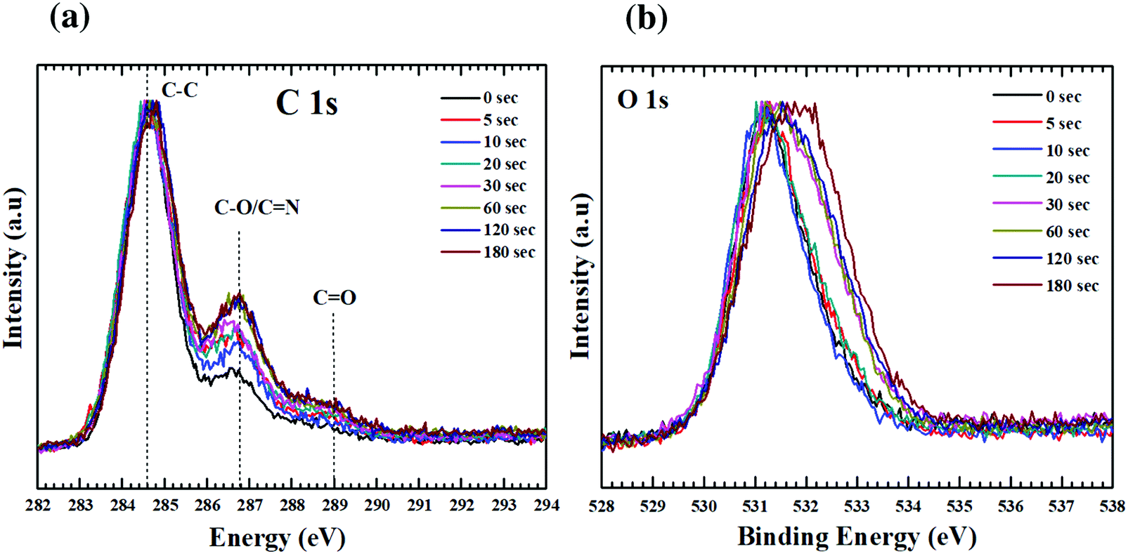 | ||
| Fig. 3 Core level photoelectron spectra for (a) carbon, (b) oxygen. Spectra from individual GO films are overlaid upon each other to recognize the effect of plasma functionalization. There is substantial changes occurring in surface chemistry of GO with plasma exposure. | ||
The contribution from different bonding environments of carbon in the graphitic structure is deconvolved using peak fitting, as shown in Fig. S2 (ESI†). Due to the semi-metallic nature of HOPG the carbon spectrum was fitted with asymmetric Doniach–Sunjic line shape. This function gives an asymptotic nature to the Doniach–Sunjic line shape function.42 While the spectra related to GO were fitted with a combined Gaussian and Lorentzian line shape functions. Table 1 presents the binding energy value along with the FWHM and percentage composition of C–C, C–O, CO components that have been used to fit the C1s spectra of GO and the functionalized GO films.
| GO sample (s) | Component | % Concentration | FWHM |
|---|---|---|---|
| 0 | C–C | 73.0 | 1.25 |
| C–O | 22.3 | 1.80 | |
| CO |
4.7 | 1.90 | |
| 5 | C–C | 69.2 | 1.28 |
| C–O | 23.8 | 2.50 | |
| CO |
7.0 | 1.90 | |
| 10 | C–C | 70.7 | 1.30 |
| C–O | 24.0 | 2.00 | |
| CO |
5.3 | 2.00 | |
| 20 | C–C | 70.3 | 1.32 |
| C–O | 23.8 | 1.75 | |
| CO |
5.8 | 1.80 | |
| 30 | C–C | 66.9 | 1.34 |
| C–O | 25.4 | 2.10 | |
| CO |
7.7 | 1.89 | |
| 60 | C–C | 63.7 | 1.35 |
| C–O | 25.8 | 2.20 | |
| CO |
10.5 | 1.60 | |
| 120 | C–C | 68.7 | 1.38 |
| C–O | 23.1 | 1.45 | |
| CO |
8.2 | 1.74 | |
| 180 | C–C | 68.3 | 1.40 |
| C–O | 24.2 | 1.50 | |
| CO |
7.5 | 1.90 | |
It has been reported that the disorder induced carbon appears at a binding energy of 0.5 eV above the graphitic sp2 carbon (284.5 eV).23 However, after considering the full width at half maxima (FWHM) of HOPG (0.72 eV) and that of the as synthesized GO (1.25 eV), it will not be a good approximation to deconvolve the C–C peak of GO into two peaks. But the absolute value of FWHM should be good measure of the increase/decrease in sp3 carbon concentration. With increased exposure to plasma this peak broadens from 1.25 eV (0 s) to 1.39 eV (180 s) as shown in Fig. 4a. This broadening can be attributed to the increase in concentration of nitrogen. The nitrogen dopants are known to increase disorder in the sp2 framework.43 Increase in CO functionalities with time during exposure to the plasma can be attributed to an increased concentration of defects. These defects originate from the impact of high energy ionic species present in the plasma. As already mentioned carbonyl/carboxyl groups found at the edge sites and dangling bonds (formed by C–C bond breaking) are more susceptible to the formation of CO species. According to Bagri et al.44 defects formed by breaking of C–C bonds in the basal plane are always decorated by the carbonyl (CO) groups. Once the C–C bond breaks, to compensate for the electron valence CO (double bond) is formed at that site.44 The fitted spectra showed a consistent trail for both these functionalities. As the C–C concentration decreased from 73 to 68%, CO increased from 4 to 9%. Despite this interplay between C–C and CO, the concentration of single bonded species showed a small increase 22 to 24%. However, the FWHM for this state (C–O) decreased by 0.5 eV (2 eV to 1.55 eV). This apparent reduction in FWHM resembles the dominance of either of C–OH or C–O–C with extended exposure to plasma.
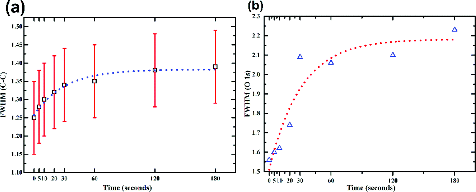 | ||
| Fig. 4 Plasma induced changes in the FWHM of (a) C–C component of fitted C1s spectrum (b) O1s spectrum. Both FWHM of C–C and O1s are saturated after 30 s, reveling the fast nature of plasma induced surface functionalisation. | ||
This increase in the C–O (single bond) moieties reflects in the O1s spectrum as increase in FWHM (as shown in Fig. 4b). As both aliphatic and aromatic C–O appears at he the higher binding energy thus broadening the O1s line shape. Previous reports suggest that carbonyl groups are formed by rearrangements of epoxy groups.45 As epoxy groups in graphene leads to a non-planar sp3 bonding configuration and creates significant strain on the neighbouring C–C bonds while CO bonds are sp2 hybridized and strain free.45 Rani et al.39 found that upon oxygen plasma treatment of GO the carbonyl components increased rather than epoxide. They inferred that the thermal energy of plasma favours clustering of the sp2 domains and oxygen atoms attach randomly, converting sp2 bonds to sp3, and as the plasma exposure increased the epoxides rearranged to form carbonyls.39 Due to low temperature associated with the plasma jet, effect of temperature can be neglected in this experiment. Nevertheless, the kinetic energy of the ions, dissociated upon impact may provide the necessary energy required for the bond rearrangements.
The reorganisation of the bonding configuration between carbon and oxygen as revealed from the carbon spectra is reflected in the oxygen spectra as well (Fig. 3b). For GO the O1s peak is positioned around 531.4 eV with an asymmetric tail (534 eV). With increasing plasma exposure, there is a significant broadening of the O1s peak along with shift toward higher binding energy. The peak contains contribution from three types of oxygen (Fig. S3, ESI†): oxygen double bonded to carbon in aromatic structure (531.3 eV), oxygen singly bonded to aliphatic carbon (532.4 eV) and oxygen singly bonded to aromatic carbon (533.3 eV). Detailed spectroscopic analysis by Ganguly et al. revealed that OH-moieties on basal plane are the most stable species.40 Thus, from the C1s and O1s spectra it can be predicted that surface epoxides are dissociating to form carbonyl and phenol groups. Nonetheless, the presence of OH radicals in the plasma may also be a reason for this change. Confirmation of this theory would need further spectroscopic studies.
The nitrogen spectra are fitted with two components at 398.8 ± 0.1 eV and 401.1 ± 0.1 eV as shown in Fig. 5(a). These correspond to pyridinic and graphitic nitrogen configurations respectively.46,47 All spectra are intensity normalized to reveal the changes in bonding environment of nitrogen with plasma functionalization. Fig. 5(b) show the relative concentration of nitrogen with respect to carbon. After 180 s of plasma exposure a nitrogen doping of 6.3% has been achieved. Additionally, the doping has been achieved while preserving the morphological of these GO films. This could prove to be major advantage while functionalising the interfaces/contact of organic devices. It is apparent from Fig. 5(a) that all functionalized samples have a prominent graphitic nitrogen signature. However, the spectral signature from pyridinic nitrogen increases until the 10 s mark and then decreases with longer plasma exposure. The variation in relative concentration of graphitic and pyridinic nitrogen is shown in Fig. 5(c). Since pyridinic nitrogen occupy the edge sites of graphene structure, it is easier to saturate the graphitic cluster with pyridinic nitrogen. While, with increased exposure to plasma, the concentration of graphitic nitrogen at the basal plane increases. Molecular dynamics (MD) simulations by XF Li et al.33 revealed that to trap nitrogen in the graphitic lattice, point defects and vacancies are crucial (a crucial process/factor). It can be interpreted from the XPS results that during the initial stage of functionalization the excited nitrogen species in the plasma tend to attack the pre-existing defects and edge sites forming both graphitic and pyridine like configurations. However, with longer exposure the energetic nitrogen species in the plasma substitute carbon in the graphitic basal plane via defect formation and results in increased concentration of stable quaternary nitrogen states.
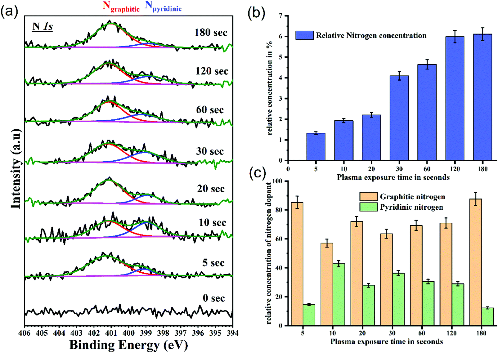 | ||
| Fig. 5 Variations in nitrogen spectra with plasma exposure time (a) fitted N1s spectra, showing presence of nitrogen in graphitic and pyridinic structure. N1s spectra consists of two components graphitic and pyridinic. Relative concentration of pyridinic nitrogen is maximum at 10 s with gradual increase in concentration of graphitic nitrogen with plasma exposure, (b) relative concentration of nitrogen with respect to carbon from the survey spectrum with respect to plasma exposure, showing increase in nitrogen in the GO framework. (c) Relative concentration of graphitic to pyridinic nitrogen from fitted N1s spectra with respect to plasma exposure. | ||
Introduction of nitrogen into the graphitic lattice influences the delocalized π electron system of graphene oxide. Nitrogen, having an excess electron, will enhance the total density of states (DOS) below the Fermi level of GO. The bonding configuration of nitrogen play a crucial role in defining this increased DOS. N in the quaternary state (sp2 N) contributes two electrons to the π system of the carbon network. Similarly, pyridine N atoms also contribute a lone pair to the π system.48 For graphitic nitrogen, of the five p electrons, three electrons are used to form σ bonds and the remaining two form bonding (π) and antibonding (π*) states.49 However, for pyridinic N the two electrons contribute to the localized N lone pair state.50
Fig. 6 presents the overlaid valence band spectra of GO and functionalized GO samples. The spectra were acquired with an incident photon energy of 230 eV. For GO, the density of states near Fermi level (0 to 4 eV) is dominated by the carbon 2p π states. The 2p σ contributions are at ∼8 eV and these two states overlap at around 6 eV binding energy. The feature at ∼13 eV corresponds to the C2s σ band and 2s–2p states hybridize at 10.6 eV.51 The inclusion of electron rich nitrogen into the carbon network would result in the formation of donor levels near the conduction band edge and hence raising the Fermi level. After careful calibration of the energy levels, it is clear from the increased intensity that the π derived states are influenced by the increased concentration of N in the system (inset of Fig. 6). This also reflects to the substitution of C–C bonds by C–N bonds. Souto et al. have found that the top of the valence band for diamond-like films undergoes profound changes upon nitrogen incorporation.48 Similar observations were also made by Luo et al. for graphene doped with pyridinic N.50
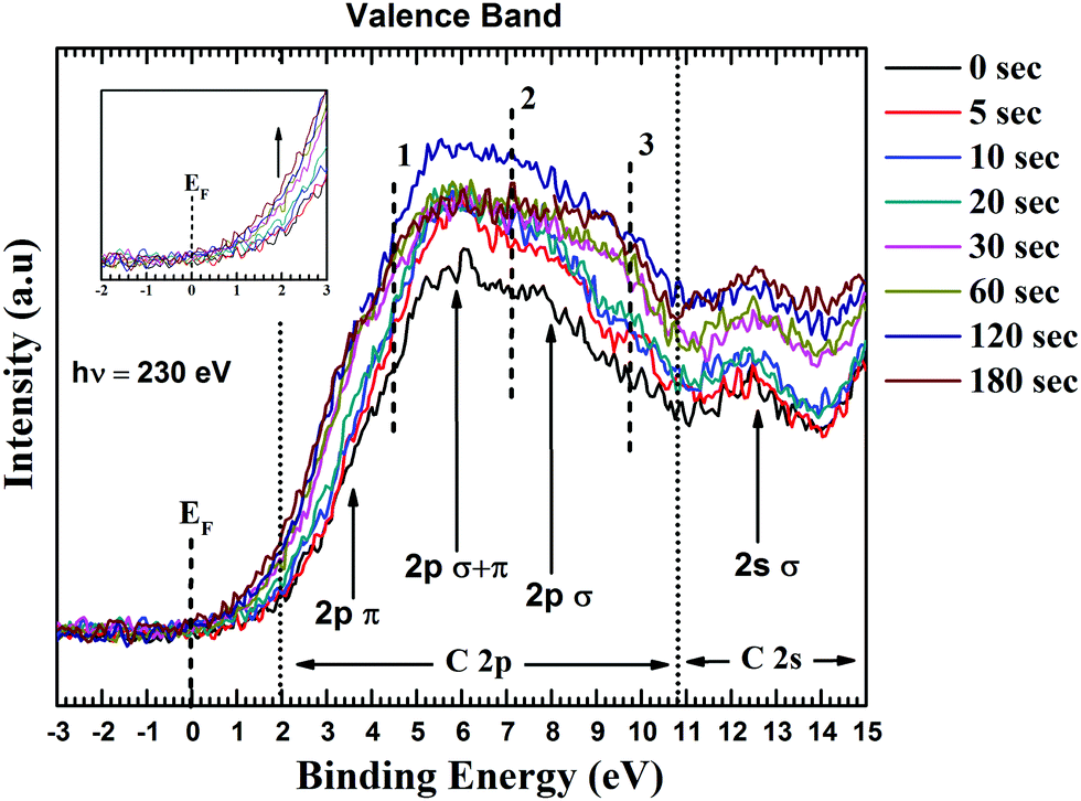 | ||
| Fig. 6 Valence band spectra of GO and functionalized GO films. The density of states are perturbed after plasma functionalisation. Showing the ability to dope nitrogen inducing changes in electronic structure of GO. | ||
The increase in DOS with nitrogen doping can be interpreted as the addition of three new bands (marked 1, 2 and 3 in Fig. 6) resulting from C–N bond formation. The band located at ∼5 eV (marked as point 1) arises from N lone pair state (a pair of electrons strongly localized on the nitrogen atom). The feature at ∼7 eV is associated with electrons occupying the π orbitals of C–N bonds while the σ orbitals of C–N bonds are located between 9.5 to 11 eV.48 As shown in Fig. 6, there is a consistent increase in the states 1, 2 and 3 until 120 s. This increasing in intensity reflects to nitrogen substitution in the graphitic lattice. However, the state 2 shows a drop in the intensity after 120 s mark. This can be due to the decrease in C–C orbital overlap of resulting from increase in C–N bonds. Luo et al. reported similar results for graphene doped with pyridinic N.50 They found that nitrogen substituted in the carbon network would enhance C–N 2p electronic states while depressing the contribution from CC 2p density of states. The DOS of states simulated by Souto et al.48 also showed similar trend, when N is progressively incorporated in the graphitic cluster. The possible reason for this decrease intensity of state 2, could be for increased nitrogen content the C–N coordination goes from a planar sp2 structure to three-dimensional sp3 structure where the N π electrons turn into nonbonding lone pairs. Thus, from valence band spectra it is apparent that there is a strong electronic coupling between the GO and the incorporated nitrogen atoms.
NEXAFS spectroscopy is a powerful tool to probe the electronic structure of GO upon functionalization using plasma jet. Here, low energy X-ray photons are used to excite core level electrons to unoccupied states above the Fermi level governed by dipole selections rules i.e. Δl = ±1. These dipole allowed transitions are highly sensitive to the local electronic structure, chemical configuration, oxidation state, molecular orientation and symmetry.52 Also, NEXAFS can provide better insight into the molecular structure than XPS. In XPS the ground state electrons are strongly perturbed by the created core hole, while in NEXAFS the screening effect is pronounced leading to negligible influence on the ground state electron cloud. In XPS the line shapes for core level features are significantly broader resulting from multiple final state transitions, whereas in NEXAFS a limited number of final states are (dipole) allowed. Thus, the overlapped features in C1s and O1s core level spectra can be easily resolved at the corresponding K-edge NEXAFS spectra.
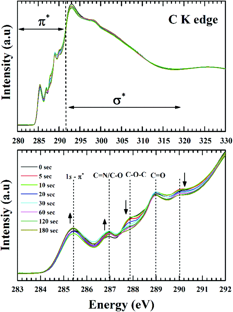
Fig. 7 shows the C K-edge NEXAFS spectra of the GO films, acquired at an incident angle of 54.7° (magic angle) of the X-ray beam. This technique has been used to negate the anisotropic orientation of π and σ states of graphitic structure. The core level transitions at 285.4 eV and 292.8 eV are representative of the π* and σ* resonances respectively from sp2 bonded CC structure. However, the absence of exciton feature at 291.65 eV is indicative of the absence of long-range order, a fact typical for GO, due to the presence of abundant defects. According to Lee et al.53 the lowest energy peak (285.4 eV) corresponds to the transition of core level C1s electrons to antibonding π states along the M–L points of the graphene Brillouin zone and the broad peak at 292.8 eV originates from transitions to the dispersion less σ states at the Γ point of graphene Brillouin zone.
 | ||
| Fig. 7 Near edge absorption of C K spectra as a function of different plasma treatment time. (a) Normalised spectra showing the π* and σ* regions, (b) expanded view of the π* region showing changes in resonances with plasma exposure. | ||
For GO the higher energy transitions (∼310 eV) are quite featureless in comparison to HOPG, the main reason being the larger interlayer distance for GO (∼1 nm) in comparison to graphite (0.34 nm).54 A smaller interlayer spacing increases scattering of the excited electron wave function by neighbouring atoms (multiple-scattering theory). Although the transitions from various functional groups are present above and below the ionization potential (IP), resonances below the IP can be more precisely defined. This is primarily because of the π* features being more prominent and intense with respect to the σ* transitions which are broader in nature and tend to overlap. For example, the peak at 292.8 eV can have contributions from π* C–O and σ* C–O absorptions along with the continuum background. Thus, a detailed analysis of the π* transitions should be definitive enough for the determination of surface chemical changes.
The region below the IP shown in Fig. 7 consists of spectral features at 290 eV, 289 eV, 287.8 eV, and 287 eV along with the CC resonance at 285.4 eV.55 The carbonyl core for the double-bonded oxygen functionalities (CO) can be associated with carboxyl or ketone environment. For carboxylic group the π* transitions are reported at 288.9 ± 0.2 eV. However, this position will shift depending on the electronegativity of the carbonyl core. For ketone groups this transitions are found at lower photon energies.55 The single-bonded oxygen functionalities in the form of phenol (–OH) and epoxy groups (C–O–C) are known to shift the π* resonance of sp2 structure to higher energy values. From the previous reported studies on graphene oxide, transition at 287 eV is due to the –OH moieties and 287.8 eV is due to epoxide moieties.26 The resonances related to C–N bonding overlaps with oxygen moieties at 287 eV and 289 eV. Dennis et al. observed the π* resonances of C–N bonds are at 286.8 eV and 288.6 eV in the C K-edge NEXAFS of imidazole.56 Due to the low atomic concentration of nitrogen and the overlapped features it's hard to delimit the absolute contribution of C–O and C–N functionalities at the C K edge. From Fig. 7 it is apparent C–N/C–O transitions are getting intense along with a noticeable drop in the intensity of epoxide resonance. This effect is in-line with the known theories of GO reduction where C–O–C are reported to be less stable than C–OH functionalities. The peak at 289 eV can be associated with the CO π* resonances in carboxyl groups (COOH). The reported values for CO transitions in GO are between 288.5 to 289 eV whereas CO in a ketone environment is found at lower energies. The feature around 290 eV can have contribution from several unresolved components. Kuznetsova et al.57 assigned this peak to σ* transitions of C–O by comparing acid-treated carbon nanotubes with 9-phenanthrol and xanthene, while Gandhiraman et al.55 associated this with Rydberg mixed OH-derived states from hydroxylated and ether-linked C-species (–O–C–OH). Seeing the trend of phenol (–OH, increasing) and epoxy groups (C–O–C, decreasing) it would be appropriate to justify this peak as epoxide derived σ* transitions of C–O.
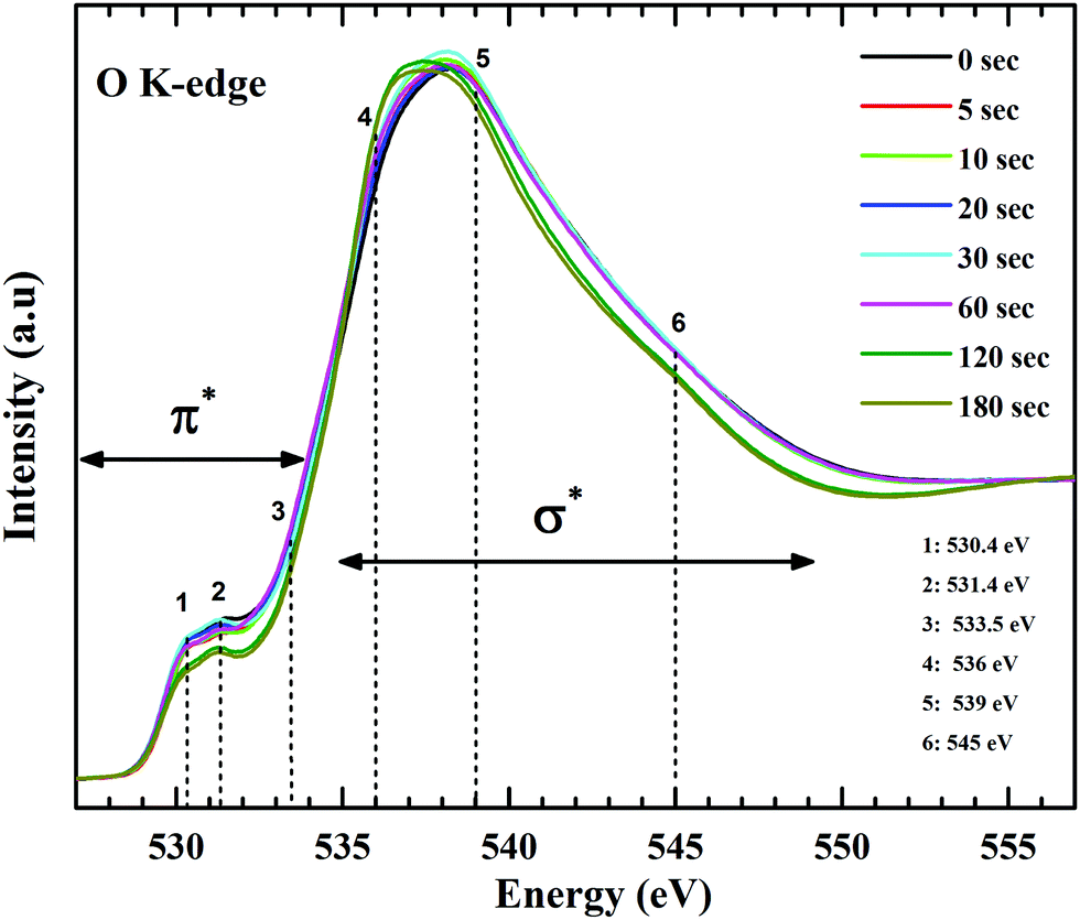
Form the carbon spectra, a presence of oxygen in different bonding environment is obvious. At the O K-edge (Fig. 8) two distinctive features are discernible, one at ∼531 eV and the other around 537 eV. The π* region has three main resonances at 530.4 eV, 531.4 eV and 532.5 eV. Lower energy absorption peaks at 530.4 eV and 531.4 eV are π* resonances form carbonyl core of carboxylic groups (–COOH).55 A feature around 533.5 eV is expected from the epoxy groups.58,59 Due to the strong oxidation process, molecules of oxygen and water get trapped between the layers of graphene oxide. X-ray absorption studies of molecular oxygen revealed that the π* resonances for O–O is at 530.8 eV.60,61 Due to prolonged plasma exposure, the defects created in the lattice might have resulted in the escape of intercalated oxygen, resulting in the intensity drop at ∼531 eV. Since, XPS measurements and C K-edge NEXAFS spectra do not reflect to the decrease in concentration of CO groups. On the other hand, the σ* region consists of rather broad and overlapped transitions. Features around 536 eV, 539 eV and 545 eV are primarily assigned to σ* states of O–H, C–O and CO of carbonyl groups respectively. The noticeable broadening observed in the O1s XPS spectra points to the increase in surface bound hydroxyl groups and can be corroborated by the O K-edge absorption spectra. The difference in spectral feature from hydroxyl-derived (O–H) σ* states validates this claim. Gradual de-epoxiation with plasma treatment is also evident for these results. As the π* and σ* transitions (regions 3 and 5) representative of C–O–C show decreased contribution in the spectra with progressive plasma exposure. The σ* transitions of C–O–C are relatively broader than other functionalities and have been reported to exist between 539 to 543 eV and the region beyond that is related to a carbonyl group (CO) bonded to an aromatic ring.
 | ||
| Fig. 8 O K-edge NEXAFS spectra of GO and functionalized GO. The changes at π* and σ* features reveals the evolution of oxygen species attached with the graphitic backbone of GO. | ||
XPS and NEXAFS changes at core level C and Oxygen show GO undergoes sufficient surface chemical modifications upon plasma functionalization. But the dissociation of the epoxy groups with increase in hydroxyl content needs an explanation. Similar phenomenon was observed by Stankovich et al. for hydrazine reduced GO.62 They proposed a mechanism in which hydrazine ring-opens epoxides to form hydrazino alcohols and eventually dissociates via the formation of an aminoaziridine moiety. In this case the ring opening might be due to the nucleophilic attack of the excited nitrogen species in the plasma. As the carbon in an epoxide ring is a strong electrophile and would result in ring opening with the formation of new C–OH and C–N bonds as shown in Fig. 9. Ring opening is also favoured due to the release of stresses in the structure.
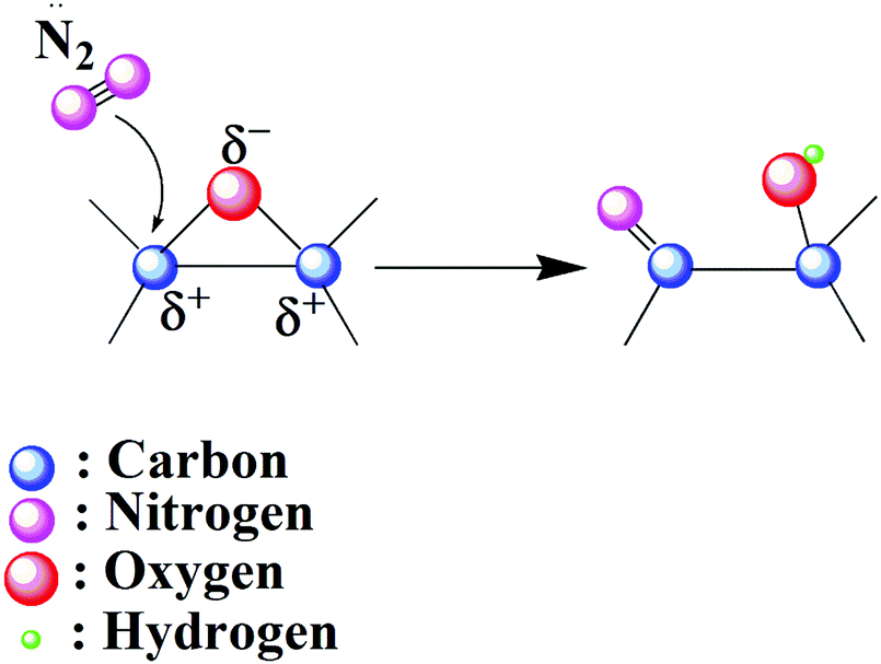 | ||
| Fig. 9 Schematics of epoxide ring opening via nucleophilic attack. Nitrogen is attracted to the carbon in an epoxide ring due to its strong electrophilic nature. | ||
Kelvin probe microscopy is a two-step process. In the first step, the AFM tip scans over the surface to take the standard topographical image, while in the second step the biased tip rises to a desired height (30 nm in this case) to take the surface potential measurements over the same area. Fig. S4 (ESI†) presents the topography image of GO and the functionalised GO films over an area of 100 μm2. All the topography images are typical for GO thin films with abundant wrinkles on the surface.63 However no substantial changes in topography could be observed from the AFM and SEM images post plasma treatment (Fig. S4 and S5, ESI†). The average roughness value of all the samples were calculated to be 3.0 ± 0.5 nm. Thus, the low power plasma used in this case does not induce noticeable physical damage (sputtering) to the GO surface, effecting only the surface electronic and chemical properties.
Introduction of nitrogen into the graphitic lattice distorts the π electron cloud, inducing shift of its Fermi level and hence influences the work function. KPFM can lead to a better understanding of the changes in the electronic properties of GO at different stages of the plasma functionalization process. In KPFM the conducting tip with an applied bias scanning over a surface is highly sensitive to any changes in local surface potential. Fig. 10(a) shows the surface potential map of pristine GO and Fig. 10(b) is the surface potential distribution over the same area. The histogram plot of the surface potential showed a Gaussian distribution profile. The mean value of this distribution can be considered as the average surface potential difference between the tip and GO film. Considering the work function of the tip to be 4.55 eV the work function of the GO film is calculated to 4.967 eV, which matches well with the reported values.64 This process was adopted to calculate the average SP for all the functionalised GO films. In SKPM it is not appropriate to quantify the measured work function values exactly with that of the sample, however the relative differences in surface potential are of an absolute nature.
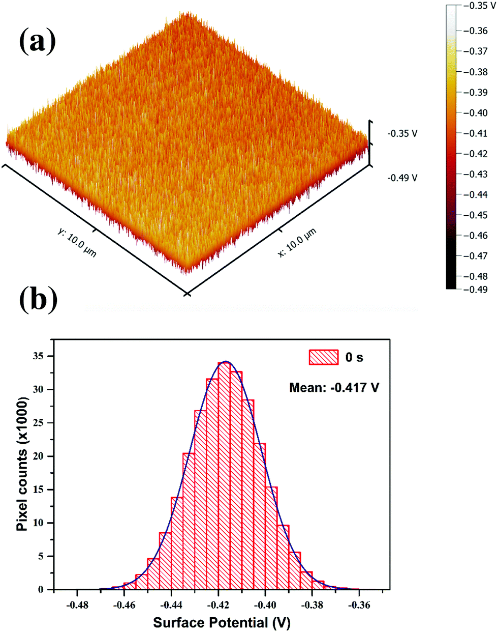 | ||
| Fig. 10 (a) KPFM surface potential map of reference GO thin film, (b) histogram plot of SP distribution of the reference GO sample; the mean value of the distribution is considered for analysis. | ||
The effect of nitrogen configuration on the electronic structure of graphene has been reported by Schiros et al.65 The nitrogen atom has five valence electrons, and in nitrogen-doped graphene the nitrogen bonds to the carbon structure via three σ bonds and one π bond. For graphitic nitrogen part of outer electrons is transferred to the surrounding carbon atoms, making the graphitic structure more electron rich (n-doping). However, for pyridinic nitrogen the electron lone pair is localised on the nitrogen atom at the edge site. Thus, the electron density over the neighbouring carbon atoms is reduce resulting in p doping.66
From Fig. 11 it is apparent that, at the initial stages (until 10 s) the work function of GO increases and with increasing nitrogen concentration the work function drops below the initial value for as-synthesised GO. This variation in SP have strong correlation with the N1s XPS spectra (Fig. 5). Here the relative concentration of pyridine nitrogen is maximum at 10 s and then gradually decreases with longer plasma exposure. The p-doping effect caused by pyridine nitrogen increases the work function of GO. But with the increase in the in-plane graphitic nitrogen the GO energy bands will be more electron rich resulting in n-type doping effect and decrease in the work function values.
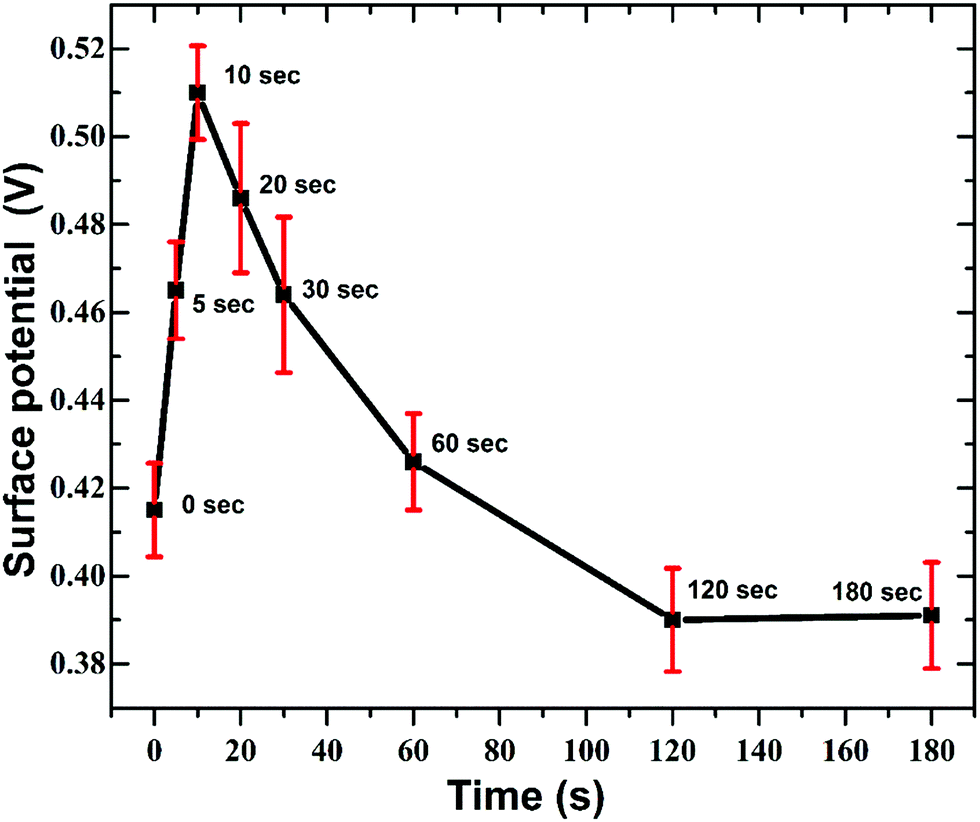 | ||
| Fig. 11 Variation in surface potential of GO with duration of APPJ treatment. The distribution reveals the transformation of GO from p-type to n-type. | ||
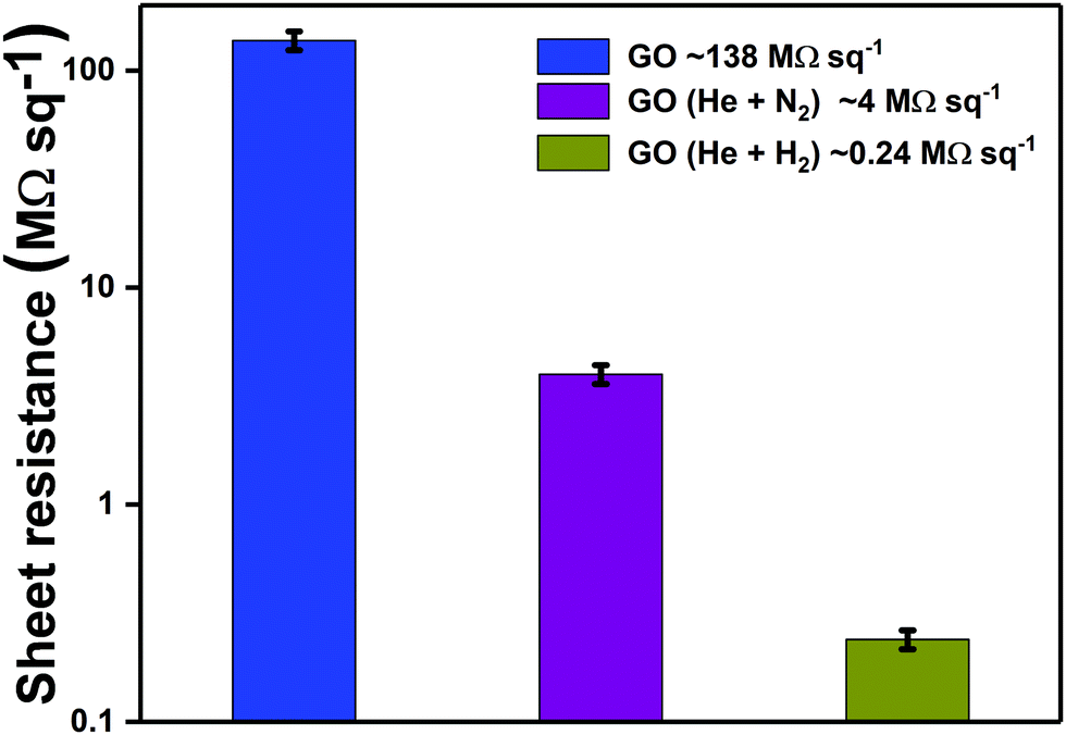
Sheet resistance measurements were undertaken to quantify the variation in film conductivity after plasma treatment. Sheet resistance of pristine GO was measured as 138.0 MΩ sq−1. The sheet resistance decreased to 4.0 MΩ sq−1 after 3 minutes of exposure to He + N2 plasma jet, indicating a 34.5× increase in conductivity. The enhancement in conductivity can be correlated with the N1s XPS spectra after 3 minutes of plasma treatment which indicates the predominance of graphitic nitrogen that makes the GO structure electron-rich (n-type). Furthermore, the GO films were treated with He + H2 plasma jet for 3 minutes which resulted in improvement in conductivity by more than two orders of magnitude (0.24 MΩ sq−1). This improved film conductivity suggests recovering of the sp2 framework upon deoxygenation of graphene oxide with He + H2 plasma jet. Reduction/deoxygenation can occur either due to the high energy electrons or ions such as He+ from the carrier gas during physical bombardment or due to the active species including hydrogen radicals (˙H), ions (He+ and H+) and neutral molecules in the plasma jet.67,68 The variation in sheet resistance of GO after treatment with different admixtures of gases can be observed in Fig. 12.
 | ||
| Fig. 12 Variation in sheet resistance of GO after treatment with APPJ generated using different gas admixtures. | ||
4. Conclusion
The properties of GO can be enhanced by various chemical and physical techniques, but they lack the promise in precision. With major advantages being clean, reliable and ideal for industrial processes, APPJ is shown to be a promising candidate for surface functionalization GO. In this study, a low power (4 W) plasma jet has been used to induce finite changes in surface chemistry and electronic properties of GO. Detailed X-ray spectroscopic studies revealed that the active species in plasma can react with GO changing its surface chemistry. The nitrogen ions can substitute carbon from the graphitic structure to form in-plane C–N bonds as revealed by the core level X-ray studies. Addition of nitrogen in the graphitic lattice introduces electronic density of states raising the Fermi level of GO. Finally, Kelvin probe studies showed that the bonding configuration can influence the work function of GO. Pyridinic nitrogen transforms GO to p-type while graphitic nitrogen increases the electron density of GO and transforming it to n type. Pointing to the fact that a low power APPJ can effectively tune the work function of GO and hence the conductivity.Author contributions
The manuscript was written through contributions of all authors. All authors have given approval to the final version of the manuscript.Funding sources
The work of A. D. and S. K. are funded by UKIERI British Council grant and Royal Academy of Engineering Industry Academia program on Recycling Lithium Ion Batteries and Plasma functionalization of solar cell from Royal Society grant.Conflicts of interest
The authors declare no competing financial interest.Acknowledgements
A. D. would also like to thank Dr Ramprasad Gandhiraman (R. P. G.) for sharing his beamtime and Dr Dennis Nordlund (beamtime scientist) for helping with the beamline experiments.References
- K. S. Novoselov, A. K. Geim, S. V. Morozov, D. Jiang, Y. Zhang, S. V. Dubonos, I. V. Grigorieva and A. A. Firsov, Electric Field Effect in Atomically Thin Carbon Films, Science, 2004, 306(5696), 666–669, DOI:10.1126/science.1102896.
- G. Eda and M. Chhowalla, Chemically Derived Graphene Oxide: Towards Large-Area Thin-Film Electronics and Optoelectronics, Adv. Mater., 2010, 22(22), 2392–2415, DOI:10.1002/adma.200903689.
- D. Chen, H. Feng and J. Li, Graphene Oxide: Preparation, Functionalization, and Electrochemical Applications, Chem. Rev., 2012, 112(11), 6027–6053, DOI:10.1021/cr300115g.
- M. Mishra, R. K. Joshi, S. Ojha, D. Kanjilal and T. Mohanty, Role of Oxygen in the Work Function Modification at Various Stages of Chemically Synthesized Graphene, J. Phys. Chem. C, 2013, 117(38), 19746–19750, DOI:10.1021/jp406712s.
- Z. Wu, S. Bai, J. Xiang, Z. Yuan, Y. Yang, W. Cui, X. Gao, Z. Liu, Y. Jin and B. Sun, Efficient Planar Heterojunction Perovskite Solar Cells Employing Graphene Oxide as Hole Conductor, Nanoscale, 2014, 6(18), 10505–10510, 10.1039/c4nr03181d.
- K. Jiao, X. Wang, Y. Wang and Y. Chen, Graphene Oxide as an Effective Interfacial Layer for Enhanced Graphene/Silicon Solar Cell Performance, J. Mater. Chem. C, 2014, 2(37), 7715, 10.1039/C4TC00705K.
- G. Eda, G. Fanchini and M. Chhowalla, Large-Area Ultrathin Films of Reduced Graphene Oxide as a Transparent and Flexible Electronic Material, Nat. Nanotechnol., 2008, 3(5), 270–274, DOI:10.1038/nnano.2008.83.
- K. P. Loh, Q. Bao, G. Eda and M. Chhowalla, Graphene Oxide as a Chemically Tunable Platform for Optical Applications, Nat. Chem., 2010, 2(12), 1015–1024, DOI:10.1038/nchem.907.
- P. K. Panda, A. Grigoriev, Y. K. Mishra and R. Ahuja, Progress in Supercapacitors: Roles of Two Dimensional Nanotubular Materials, Nanoscale Adv., 2019, 2, 70–108, 10.1039/C9NA00307J.
- R. Garg, N. Dutta and N. Choudhury, Work Function Engineering of Graphene, Nanomaterials, 2014, 4(2), 267–300, DOI:10.3390/nano4020267.
- P. V. Kumar, M. Bernardi and J. C. Grossman, The Impact of Functionalization on the Stability, Work Function, and Photoluminescence of Reduced Graphene Oxide, ACS Nano, 2013, 7(2), 1638–1645, DOI:10.1021/nn305507p.
- L. Sygellou, G. Paterakis, C. Galiotis and D. Tasis, Work Function Tuning of Reduced Graphene Oxide Thin Films, J. Phys. Chem. C, 2015, 120(1), 281–290, DOI:10.1021/acs.jpcc.5b09234.
- A. Benayad, H. J. Shin, H. K. Park, S. M. Yoon, K. K. Kim, M. H. Jin, H. K. Jeong, J. C. Lee, J. Y. Choi and Y. H. Lee, Controlling Work Function of Reduced Graphite Oxide with Au-Ion Concentration, Chem. Phys. Lett., 2009, 475(1–3), 91–95, DOI:10.1016/j.cplett.2009.05.023.
- J. Li, X. Qi, G. Hao, L. Ren and J. Zhong, In-Situ Investigation of Graphene Oxide under UV Irradiation: Evolution of Work Function, AIP Adv., 2015, 5(6), 067154, DOI:10.1063/1.4923238.
- C.-Y. Lin, C.-E. Cheng, S. Wang, H. W. Shiu, L. Y. Chang, C.-H. Chen, T.-W. Lin, C.-S. Chang and F. S.-S. Chien, Synchrotron Radiation Soft X-Ray Induced Reduction in Graphene Oxide Characterized by Time-Resolved Photoelectron Spectroscopy, J. Phys. Chem. C, 2015, 119(23), 12910–12915, DOI:10.1021/jp512055g.
- B. Kang, S. Lim, W. H. Lee, S. B. Jo and K. Cho, Work-Function-Tuned Reduced Graphene Oxide via Direct Surface Functionalization as Source/Drain Electrodes in Bottom-Contact Organic Transistors, Adv. Mater., 2013, 25(41), 5856–5862, DOI:10.1002/adma.201302358.
- H. Wang, T. Maiyalagan and X. Wang, Review on Recent Progress in Nitrogen-Doped Graphene: Synthesis, Characterization, and Its Potential Applications, ACS Catal., 2012, 2(5), 781–794, DOI:10.1021/cs200652y.
- A. Dey, A. Chroneos, N. S. J. Braithwaite, R. P. Gandhiraman and S. Krishnamurthy, Plasma Engineering of Graphene, Appl. Phys. Rev., 2016, 3(2), 021301, DOI:10.1063/1.4947188.
- J. Laimer and H. Störi, Recent Advances in the Research on Non-Equilibrium Atmospheric Pressure Plasma Jets, Plasma Processes Polym., 2007, 4(3), 266–274, DOI:10.1002/ppap.200600114.
- H.-W. Liu, S.-P. Liang, T.-J. Wu, H. Chang, P.-K. Kao, C.-C. Hsu, J.-Z. Chen, P.-T. Chou and I.-C. Cheng, Rapid Atmospheric Pressure Plasma Jet Processed Reduced Graphene Oxide Counter Electrodes for Dye-Sensitized Solar Cells, ACS Appl. Mater. Interfaces, 2014, 6(17), 15105–15112, DOI:10.1021/am503217f.
- F. Alotaibi, T. T. Tung, M. J. Nine, S. Kabiri, M. Moussa, D. N. H. Tran and D. Losic, Scanning Atmospheric Plasma for Ultrafast Reduction of Graphene Oxide and Fabrication of Highly Conductive Graphene Films and Patterns, Carbon, 2018, 127, 113–121, DOI:10.1016/j.carbon.2017.10.075.
- B.-J. Lee, S.-C. Cho and G.-H. Jeong, Atmospheric Pressure Plasma Treatment on Graphene Grown by Chemical Vapor Deposition, Curr. Appl. Phys., 2015, 15(5), 563–568, DOI:10.1016/j.cap.2015.02.013.
- W. Huang and S. Ptasinska, Functionalization of Graphene by Atmospheric Pressure Plasma Jet in Air or H2O2 Environments, Appl. Surf. Sci., 2016, 367, 160–166, DOI:10.1016/j.apsusc.2016.01.170.
- M. Fu, Q. Jiao, Y. Zhao and H. Li, Vapor Diffusion Synthesis of CoFe2O4 Hollow Sphere/Graphene Composites as Absorbing Materials, J. Mater. Chem. A, 2014, 2(3), 735–744, 10.1039/C3TA14050D.
- K. G. Tirsell and V. P. Karpenko, A General Purpose Sub-KeV X-Ray Facility at the Stanford Synchrotron Radiation Laboratory, Nucl. Instrum. Methods Phys. Res., Sect. A, 1990, 291(1–2), 511–517, DOI:10.1016/0168-9002(90)90113-K.
- B. J. Schultz, R. V. Dennis, J. P. Aldinger, C. Jaye, X. Wang, D. A. Fischer, A. N. Cartwright and S. Banerjee, X-Ray Absorption Spectroscopy Studies of Electronic Structure Recovery and Nitrogen Local Structure upon Thermal Reduction of Graphene Oxide in an Ammonia Environment, RSC Adv., 2014, 4(2), 634–644, 10.1039/C3RA45591B.
- D. A. Shirley, High-Resolution x-Ray Photoemission Spectrum of the Valence Bands of Gold, Phys. Rev. B: Solid State, 1972, 5(12), 4709–4714, DOI:10.1103/PhysRevB.5.4709.
- (a) D. Marinov and N. S. J. Braithwaite, Power Coupling and Electrical Characterization of a Radio-Frequency Micro Atmospheric Pressure Plasma Jet, Plasma Sources Sci. Technol., 2014, 23(6), 062005, DOI:10.1088/0963-0252/23/6/062005; (b) J. Golda, J. Held, B. Redeker, M. Konkowski, P. Beijer, A. Sobota, G. Kroesen, N. St. J. Braithwaite, S. Reuter, M. M. Turner, T. Gans, D. O'Connell and V. Schulz-von der Gathen, Concepts and characteristics of the “COST Reference Microplasma Jet”, J. Phys. D: Appl. Phys., 2016, 49(8), 084003, DOI:10.1088/0022-3727/49/8/084003.
- K. J. Clay, S. P. Speakman, G. A. J. Amaratunga and S. R. P. Silva, Characterization of A-C:H:N Deposition from CH4/N2 Rf Plasmas Using Optical Emission Spectroscopy, J. Appl. Phys., 1996, 79(9), 7227–7233, DOI:10.1063/1.361439.
- M. K. Singh, A. Ogino and M. Nagatsu, Inactivation Factors of Spore-Forming Bacteria Using Low-Pressure Microwave Plasmas in an N2 and O2 Gas Mixture, New J. Phys., 2009, 11(11), 115027, DOI:10.1088/1367-2630/11/11/115027.
- V. Arkhipenko, A. Kirillov, L. Simonchik and S. Zgirouski, Influence of Nitrogen Impurities on an Electron-Excited Helium Atoms Concentration in the Self-Sustained Normal Dc Glow Discharge at Atmospheric Pressure. 12th International Congress on Plasma Physics, 2004, pp. 1–10.
- L. Lai, J. R. Potts, D. Zhan, L. Wang, C. K. Poh, C. Tang, H. Gong, Z. Shen, J. Lin and R. S. Ruoff, Exploration of the Active Center Structure of Nitrogen-Doped Graphene-Based Catalysts for Oxygen Reduction Reaction, Energy Environ. Sci., 2012, 5(7), 7936, 10.1039/c2ee21802j.
- X.-F. Li, K.-Y. Lian, L. Liu, Y. Wu, Q. Qiu, J. Jiang, M. Deng and Y. Luo, Unraveling the Formation Mechanism of Graphitic Nitrogen-Doping in Thermally Treated Graphene with Ammonia, Sci. Rep., 2016, 6, 23495, DOI:10.1038/srep23495.
- R. Lv, Q. Li, A. R. Botello-Méndez, T. Hayashi, B. Wang, A. Berkdemir, Q. Hao, A. L. Elías, R. Cruz-Silva and H. R. Gutiérrez, et al., Nitrogen-Doped Graphene: Beyond Single Substitution and Enhanced Molecular Sensing, Sci. Rep., 2012, 2, 586, DOI:10.1038/srep00586.
- Y. Zhao, R. Nakamura, K. Kamiya, S. Nakanishi and K. Hashimoto, Nitrogen-Doped Carbon Nanomaterials as Non-Metal Electrocatalysts for Water Oxidation, Nat. Commun., 2013, 4, 1–7, DOI:10.1038/ncomms3390.
- X.-F. Li, K.-Y. Lian, Q. Qiu and Y. Luo, Half-Filled Energy Bands Induced Negative Differential Resistance in Nitrogen-Doped Graphene, Nanoscale, 2015, 7(9), 4156–4162, 10.1039/C4NR07472F.
- T. Hu, X. Sun, H. Sun, G. Xin, D. Shao, C. Liu and J. Lian, Rapid Synthesis of Nitrogen-Doped Graphene for a Lithium Ion Battery Anode with Excellent Rate Performance and Super-Long Cyclic Stability, Phys. Chem. Chem. Phys., 2014, 16(3), 1060–1066, 10.1039/c3cp54494j.
- NIST X-ray Photoelectron Spectroscopy (XPS) Database Main Search Menu, https://srdata.nist.gov/xps/main_search_menu.aspx, accessed Jun 18, 2017.
- J. R. Rani, J. Lim, J. Oh, J. W. Kim, H. S. Shin, J. H. Kim, S. Lee and S. C. Jun, Epoxy to Carbonyl Group Conversion in Graphene Oxide Thin Films: Effect on Structural and Luminescent Characteristics, J. Phys. Chem. C, 2012, 116(35), 19010–19017, DOI:10.1021/jp3050302.
- A. Ganguly, S. Sharma, P. Papakonstantinou and J. Hamilton, Probing the Thermal Deoxygenation of Graphene Oxide Using High-Resolution In Situ X-Ray-Based Spectroscopies, J. Phys. Chem. C, 2011, 115(34), 17009–17019, DOI:10.1021/jp203741y.
- A. Lerf, H. He, M. Forster and J. Klinowski, Structure of Graphite Oxide Revisited, J. Phys. Chem. B, 1998, 102(23), 4477–4482, DOI:10.1021/jp9731821.
- S. Doniach and M. Sunjic, Many-Electron Singularity in X-Ray Photoemission and X-Ray Line Spectra from Metals, J. Phys. C: Solid State Phys., 1970, 3(2), 285–291, DOI:10.1088/0022-3719/3/2/010.
- X. Li, H. Wang, J. T. Robinson, H. Sanchez, G. Diankov and H. Dai, Simultaneous Nitrogen Doping and Reduction of Graphene Oxide, J. Am. Chem. Soc., 2009, 131(43), 15939–15944, DOI:10.1021/ja907098f.
- A. Bagri, R. Grantab, N. V. Medhekar and V. B. Shenoy, Stability and Formation Mechanisms of Carbonyl-and Hydroxyl-Decorated Holes in Graphene Oxide, J. Phys. Chem. C, 2010, 114(28), 12053–12061, DOI:10.1021/jp908801c.
- A. Bagri, C. Mattevi, M. Acik, Y. J. Chabal, M. Chhowalla and V. B. Shenoy, Structural Evolution during the Reduction of Chemically Derived Graphene Oxide, Nat. Chem., 2010, 2(7), 581–587, DOI:10.1038/nchem.686.
- J. Moon, J. An, U. Sim, S. P. Cho, J. H. Kang, C. Chung, J. H. Seo, J. Lee, K. T. Nam and B. H. Hong, One-Step Synthesis of N-Doped Graphene Quantum Sheets from Monolayer Graphene by Nitrogen Plasma, Adv. Mater., 2014, 26(21), 3501–3505, DOI:10.1002/adma.201306287.
- D. Usachov, O. Vilkov, A. Grüneis, D. Haberer, A. Fedorov, V. K. Adamchuk, A. B. Preobrajenski, P. Dudin, A. Barinov and M. Oehzelt, et al., Nitrogen-Doped Graphene: Efficient Growth, Structure, and Electronic Properties, Nano Lett., 2011, 11(12), 5401–5407, DOI:10.1021/nl2031037.
- S. Souto, M. Pickholz, M. dos Santos and F. Alvarez, Electronic Structure of Nitrogen-Carbon Alloys (a-CNx) Determined by Photoelectron Spectroscopy, Phys. Rev. B: Condens. Matter Mater. Phys., 1998, 57(4), 2536–2540, DOI:10.1103/PhysRevB.57.2536.
- Y. Li, Z. Zhou, P. Shen and Z. Chen, Spin Gapless Semiconductor-Metal-Half-Metal Properties in Nitrogen-Doped Zigzag Graphene Nanoribbons, ACS Nano, 2009, 3(7), 1952–1958, DOI:10.1021/nn9003428.
- Z. Luo, S. Lim, Z. Tian, J. Shang, L. Lai, B. MacDonald, C. Fu, Z. Shen, T. Yu and J. Lin, Pyridinic N Doped Graphene: Synthesis, Electronic Structure, and Electrocatalytic Property, J. Mater. Chem., 2011, 21, 8038, 10.1039/c1jm10845j.
- Z. Luo, J. Shang, S. Lim, D. Li, Q. Xiong, Z. Shen, J. Lin and T. Yu, Modulating the Electronic Structures of Graphene by Controllable Hydrogenation, Appl. Phys. Lett., 2010, 97(23), 2010–2012, DOI:10.1063/1.3524217.
- G. Hahner, Near Edge X-Ray Absorption Fine Structure Spectroscopy as a Tool to Probe Electronic and Structural Properties of Thin Organic Films and Liquids, Chem. Soc. Rev., 2006, 35(12), 1244–1255, 10.1039/b509853j.
- V. Lee, R. V. Dennis, B. J. Schultz, C. Jaye, D. A. Fischer and S. Banerjee, Soft X-Ray Absorption Spectroscopy Studies of the Electronic Structure Recovery of Graphene Oxide upon Chemical Defunctionalization, J. Phys. Chem. C, 2012, 116(38), 20591–20599, DOI:10.1021/jp306497f.
- D. Pacilé, J. C. Meyer, A. Fraile Rodríguez, M. Papagno, C. Gómez-Navarro, R. S. Sundaram, M. Burghard, K. Kern, C. Carbone and U. Kaiser, Electronic Properties and Atomic Structure of Graphene Oxide Membranes, Carbon, 2011, 49(3), 966–972, DOI:10.1016/j.carbon.2010.09.063.
- R. P. Gandhiraman, D. Nordlund, C. Javier, J. E. Koehne, B. Chen and M. Meyyappan, X-Ray Absorption Study of Graphene Oxide and Transition Metal Oxide Nanocomposites, J. Phys. Chem. C, 2014, 118(32), 18706–18712, DOI:10.1021/Jp503941t.
- R. V. Dennis, B. J. Schultz, C. Jaye, X. Wang, D. A. Fischer, A. N. Cartwright and S. Banerjee, Near-Edge X-Ray Absorption Fine Structure Spectroscopy Study of Nitrogen Incorporation in Chemically Reduced Graphene Oxide, J. Vac. Sci. Technol. B Microelectron. Nanom. Struct., 2013, 31, 041204, DOI:10.1116/1.4813058.
- A. Kuznetsova, I. Popova, J. T. Yates, M. J. Bronikowski, C. B. Huffman, J. Liu, R. E. Smalley, H. H. Hwu and J. G. Chen, Oxygen-Containing Functional Groups on Single-Wall Carbon Nanotubes: NEXAFS and Vibrational Spectroscopic Studies, J. Am. Chem. Soc., 2001, 123(43), 10699–10704, DOI:10.1021/ja011021b.
- H.-K. K. Jeong, H.-J. J. Noh, J.-Y. Y. Kim, M. H. Jin, C. Y. Park and Y. H. Lee, X-Ray Absorption Spectroscopy of Graphite Oxide, EPL, 2008, 82(6), 67004, DOI:10.1209/0295-5075/82/67004.
- L. Zhang, L. Ji, P.-A. Glans, Y. Zhang, J. Zhu and J. Guo, Electronic Structure and Chemical Bonding of a Graphene Oxide-Sulfur Nanocomposite for Use in Superior Performance Lithium-Sulfur Cells, Phys. Chem. Chem. Phys., 2012, 14(39), 13670–13675, 10.1039/c2cp42866k.
- J. Chen, C. L. Lin, S. L. Qiu, M. Strongin and M. L. denBoer, Auger and X-ray Absorption Studies of Solid Molecular Oxygen, J. Vac. Sci. Technol., A, 1990, 8(3), 2591–2594, DOI:10.1116/1.576676.
- F. Matsui, H. W. Yeom, K. Amemiya, K. Tono and T. Ohta, Reinterpretation of the Molecular O2 Chemisorbate in the Initial Oxidation of the Si(111)7 × 7 Surface, Phys. Rev. Lett., 2000, 85(3), 630–633 CrossRef CAS PubMed.
- S. Stankovich, D. A. Dikin, R. D. Piner, K. A. Kohlhaas, A. Kleinhammes, Y. Jia, Y. Wu, S. T. Nguyen and R. S. Ruoff, Synthesis of Graphene-Based Nanosheets via Chemical Reduction of Exfoliated Graphite Oxide, Carbon, 2007, 45(7), 1558–1565, DOI:10.1016/j.carbon.2007.02.034.
- S. E. Yalcin, C. Galande, R. Kappera, H. Yamaguchi, U. Martinez, K. A. Velizhanin, S. K. Doorn, A. M. Dattelbaum, M. Chhowalla and P. M. Ajayan, et al., Direct Imaging of Charge Transport in Progressively Reduced Graphene Oxide Using Electrostatic Force Microscopy, ACS Nano, 2015, 9(3), 2981–2988, DOI:10.1021/nn507150q.
- E. Stratakis, K. Savva, D. Konios, C. Petridis and E. Kymakis, Improving the Efficiency of Organic Photovoltaics by Tuning the Work Function of Graphene Oxide Hole Transporting Layers, Nanoscale, 2014, 6(12), 6925–6931, 10.1039/c4nr01539h.
- T. Schiros, D. Nordlund, L. Pálová, D. Prezzi, L. Zhao, K. S. Kim, U. Wurstbauer, C. Gutiérrez, D. Delongchamp and C. Jaye, et al., Connecting Dopant Bond Type with Electronic Structure in N-Doped Graphene, Nano Lett., 2012, 12(8), 4025–4031, DOI:10.1021/nl301409h.
- K. Akada, T. Terasawa, G. Imamura, S. Obata and K. Saiki, Control of Work Function of Graphene by Plasma Assisted Nitrogen Doping, Appl. Phys. Lett., 2014, 104, 131602, DOI:10.1063/1.4870424.
- S. W. Lee, C. Mattevi, M. Chhowalla and R. M. Sankaran, Plasma-Assisted Reduction of Graphene Oxide at Low Temperature and Atmospheric Pressure for Flexible Conductor Applications, J. Phys. Chem. Lett., 2012, 3(6), 772–777, DOI:10.1021/jz300080p.
- L. Chandana, P. Ghosal and S. Challapalli, Improved Solar Cell Performance of High Quality Plasma Reduced Graphene Oxide, Plasma Processes Polym., 2016, 13(9), 929–936 CrossRef CAS.
Footnote |
| † Electronic supplementary information (ESI) available. See DOI: 10.1039/c9cp06174f |
| This journal is © the Owner Societies 2020 |