
Three-dimensional line edge roughness in pre- and post-dry etch line and space patterns of block copolymer lithography†
Shubham
Pinge
a,
Yufeng
Qiu
a,
Victor
Monreal
b,
Durairaj
Baskaran
b,
Abhaiguru
Ravirajan
a and
Yong Lak
Joo
 *a
*a
aRobert Frederick Smith School of Chemical and Biomolecular Engineering, Cornell University, Ithaca, NY 14853, USA. E-mail: ylj2@cornell.edu
bEMD Performance Materials Corp., 70 Meister Avenue, Somerville, NJ 08876, USA
First published on 2nd December 2019
Abstract
In this work, we employ large-scale coarse-grained molecular dynamics (CGMD) simulations to study the three-dimensional line edge roughness associated with line and space patterns of chemo-epitaxially directed symmetric block copolymers (BCPs) on a flat substrate. The di-block copolymer chain length and interaction parameters are validated with the experimental BCP period, L0 and corresponding molecular weight. Defect-free lamellae are formed, after which the system is quenched below the glass transition temperature before selectively dry-etching off one of the BCP phases. The effect of varying etch-selectivity on post-etch resist domain morphology was studied. The roughness of the polymer domain was evaluated over three process stages: annealing, pre-etching, and post-etching. Power spectral density plots were then generated to elucidate the contributions of low and high frequency roughness for the three process stages. The roughness results obtained from simulations are shown to be in close agreement with the roughness result obtained from analyzing experimental SEM images. Parameters like the Hurtz roughness exponent and correlation length inherent to the process and the BCP were also revealed from the experimental study.
I. Introduction
Over the past decade, with the ever-increasing demand for miniaturization of micro-electronic devices, directed self-assembly (DSA) of block copolymers (BCPs) has attracted the interest of both academia and industry to develop optimal, defect-free nanolithographic patterns due to its low cost. Also, it is not restricted by inherent diffraction-based limitations.1–5 The periodic spatial arrangement of the micro-phase separated bulk BCP6 is seldom perfectly achieved without it being directed. In the semiconductor industry, two of the popular techniques that are used are graphoepitaxy,7–9 which uses surface features and confinement to direct the BCP, and chemoepitaxy,3,10–13 which uses enthalpic interactions via chemical patterning to control the BCP ordering. Compared with chemoepitaxy, graphoepitaxy is harder to perform on a large scale to get a lamellar structure, and it is more often used to get ordered cylindrical domains or smaller-scale lamellar structures. Among chemoepitaxial technologies to form line-space patterns, Liu–Nealey (LiNe) flow with near symmetric polystyrene-block-polymethyl methacrylate (PS-b-PMMA) has been widely considered as a prospective DSA candidate for commercialization.12,13 The PS-pinned region is patterned with cross-linked PS mat film while the rest of the substrate is grafted by random hydroxyl terminated PS-co-PMMA chains (neutral layer) usually of a lower chain length than the PS mat. PS-b-PMMA BCP is then spin coated on top of this chemically patterned substrate and annealed at elevated temperatures (250–300 °C) to obtain defect-free BCP lamellae.Once this ideal lamellar morphology is formed, PMMA is selectively removed, forming a nano-lithographic pattern template of the remaining PS domain. This exercise leaves the patterned substrate exposed and can be further processed for semiconductor applications. The etching process can either be performed with a selective solvent like acetic acid (wet-etching) or using a variety of plasma etches (dry-etching) such as O2/Ar.14–17 While wet-etching is more selective than dry-etching, it has a tendency of pattern collapse, especially for high BCP film thicknesses and low solvent conditions due to the diverging surface forces during solvent evaporation. Therefore, even though dry-etching has substantially lower selectivity, using plasma ions has been preferred over the more economical wet-etching for line and space patterns.
In dry-etching, a lower ion to radical ratio leads to rougher surfaces. Ion bombardment removes PMMA by striking the material with high energy etch ions forming volatile products like CO and CO2. These volatile products are enhanced by the presence of Ar ions, which break bonds on the surface and depolymerize PMMA, leading to high etch rates.18–20 This removal of materials also causes the formation of dangling bonds that have the ability to recombine with newly exposed surface or residual material, forming a cross-linked polymer mini-networks and increasing the etch-resistance to subsequent ion-bombardment. This tendency to cross-link is higher for PS than PMMA and plays a crucial role in affecting the surface morphology of the etched material.20–24 On the other hand, oxygen radical reacts with the oxygen groups to chemically remove PMMA. These radicals are often known to form a passive inhibition layer as a byproduct. The presence of Ar ion in addition to O2 radicals helps in the removal of this inhibition layer,24 and as a result, increases the PMMA removing rate.
The anisotropic imperfections caused by the etching process coupled with the inherent BCP interfacial width leads to line-edge roughness (LER) and line-width roughness (LWR) in the line- and space-patterns. LER is defined as the 3σ deviation of a line-edge from the mean straight line. High LER values in features lead to hindrance in the flow of electrons leading to anomalies in the device resistance and capacitances, making the device inviable.25,26 The 2015 International Technology Roadmap for Semiconductors has listed DSA among one of the top prospective next-generation lithographic alternatives, but the current high 3σ LER values need further improvements for its commercialization.27 To achieve this goal, it is important to characterize and quantify the roughness along the film thickness as opposed to the approximated top-down values obtained from SEM images.
Modeling and simulations can aid the manufacturer in this regard. A wide range of DSA modeling work has been achieved using a self-consistent field (SCF) approach or theoretically informed coarse-grained (TICG) framework.28,29 While SCFT has been prevalently used over the years to predict the theoretical BCP phase diagrams, interfacial width cannot be accurately measured if the fluctuations are not accounted for. The TICG framework with its improvised strategies considers fluctuations and has been popularly used in recent years to study chemoepitaxial DSA, and especially to predict the energetics of defect annihilation.30,31 Owing to the higher degree of coarse-graining, the roughness values computed using the TICG framework or an allied methodology like single-chain-in-mean-field (SCMF) simulations are limited to low frequency estimations in the frequency domain. Daoulas and co-authors have studied the effect of roughness of the patterned substrate and its propagation through the film thickness, for undulated and peristaltic low frequency variation using a SCMF approach with successful comparison with experiments.32,33 Recently, Segal-Peretz et al. have demonstrated the implementation of the TICG framework in conjunction with scanning transmission electron microscopy to characterize the three-dimensional structure of DSA with high-χ BCP, P2VP-b-PS-b-P2VP.34 Coarse-grained polymer field-theoretic simulations have also been employed by Bosse and co-authors to predict the interfacial fluctuations for BCP resists with a peak in the spectral plots at the BCP interdomain spacing.27 Although these simulations are computationally economical, the authors categorically state their limitations in characterizing high frequency roughness and suggest the need for an intensive particle based molecular dynamics (MD) approach for a more complete understanding. Among the few available MD literature reports on the subject, there is a lack of matching of the BCP chain length to the actual molecular weight and the corresponding experimental BCP pitch (Lexp0).35,36 More importantly, none of the above stated works study the resist morphology evaluation after etching one of the BCP phases. While characterizing the interfacial deviations is crucial, the actual pattern transfer to the underlying silicon substrate takes place with the removal of the non-resist BCP phase.
In this work, we have used large-scale coarse-grained molecular dynamics (CGMD) simulations with close matching of experimental and simulation BCP molecular weights, and substrate dimensions to study the 3-dimensional BCP morphologies of DSA with LiNe flow over three process stages: after annealing, after quenching below the glass transition of BCP (pre-etch), and after selective dry-etching of the PMMA phase (post-etch).
II. Models and methods
Simulation system overview
A flat, patterned substrate was used for the LiNe flow simulations. The patterned part of the substrate is selective to PS while the unpatterned part is neutral. The selectively patterned substrate that corresponds to the cross-linked PS mat (red part in Fig. 1a) has a pinning width (pw) = 16 nm (∼0.57L0) and a density multiplication of 3×, indicating 3 domains each of PS and PMMA per patterning. The non-patterned part of the substrate (yellow part in Fig. 1a) that mimics the neutral brush in experiments is non-selective towards either of the phases. Fig. 1b shows the post-anneal BCP morphology profiles.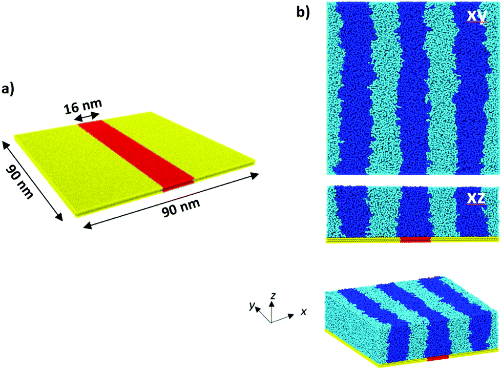 | ||
| Fig. 1 (a) CGMD simulations of a flat substrate and (b) morphology profile after annealing (Tanneal = 1.2). PS mat shown in red, neutral brush shown in yellow, PS domain shown in blue, and PMMA domain shown in cyan. | ||
On the top of the BCP domain, there is a neutral top layer (not shown in Fig. 1) to prevent BCP beads from escaping the simulation box in the z direction. This top substrate has the same properties and interaction parameters as the neutral part of the bottom substrate.
Simulation system parameters
The polymer chain is modeled as an AB block with both monomer radii (σ′) equal to 1 nm. In block A, each bead contains 4 monomers of PS while in block B, each bead contains 4.5 monomers of PMMA to account for the difference in bulk densities of the two monomers. Each polymer chain comprises 63 beads of PS (∼26![[thin space (1/6-em)]](https://www.rsc.org/images/entities/char_2009.gif) 000 g mol−1) and 58 beads of PMMA (∼26000 g mol−1). The reduced mass of each bead is adjusted according to the respective coarsening for PS and PMMA. The interaction between bonded BCP beads is given by the fene bond potential in eqn (1), where K = 30εσ′−2 is the spring constant of the BCP bond while Rmax = 1.5σ′ is the maximum bond extensibility.38
000 g mol−1) and 58 beads of PMMA (∼26000 g mol−1). The reduced mass of each bead is adjusted according to the respective coarsening for PS and PMMA. The interaction between bonded BCP beads is given by the fene bond potential in eqn (1), where K = 30εσ′−2 is the spring constant of the BCP bond while Rmax = 1.5σ′ is the maximum bond extensibility.38| Ufene(r) = −0.5KRmax2ln[1 − (r/Rmax)2] | (1) |
The favorable long-range interactions are governed by a tail-corrected Lennard Jones interaction9 given by eqn (2) while the repulsive interaction is in accordance with Weeks–Chandler–Andersen39 (WCA) potential as eqn (3).
| Uattractive(r) = 4ε[(σ′/r)12 − (σ′/r)6] + SLJ(r) for r < 2.5σ′ | (2) |
| Urepulsive(r) = 4ε[(σ′/r)12 − (σ′/r)6] + ε for r < 21/6σ′ | (3) |
A global BCP site density of 0.85 beads nm−3 is maintained and the thermostat employed is Nosé–Hoover. The BCP in the study corresponds to PS-b-PMMA with Lexp0 = 28 nm. Bulk trials were performed varying the Lennard Jones interaction parameter εBCP–BCP to elucidate parameters for Lsim0–Lexp0 for various chain lengths. The optimized parameters from the bulk study, εPS–PS,attractive = 0.15, εPMMA–PMMA,attractive = 0.15, and εPS–PMMA,repulsive = 0.15, were used for the main simulations. The simulation box is periodic in x and y and fixed in z with a BCP film thickness the same as L0 = 28 nm. The substrate is three-layer thick (3σ′) with hexagonal packing. As the maximum cut-off radius for any interaction is 2.5σ′, any thickness greater than 2.5σ′ will not affect the BCP morphology. The neutral substrate beads interact with the BCP with Uattractive(r). The pinned substrate interacts with PS beads by Uattractive(r) and with PMMA beads by Urepulsive(r). The default interaction strength of the neutral brush and pinned area with the BCP: εBCP-neutral = 0.15, εPS-pinned,attractive = 0.15, and εPMMA-pinned,repulsive = 0.15.
Independent bulk trials were performed with only the PS part of the BCP (N63) and the mean squared displacement of the equilibrated melt was plotted for temperatures ranging from 0.1 to 1.2.37 The point of change in the slope of the curve thus generated denoted the glass transition temperature Tg ∼ 0.3.
Different simulation stages
In the first stage of the process, the system is annealed at Tanneal = 1.2 to form defect-free lamellae. Since this temperature is substantially higher than the glass transition temperature, similar to the experimental temperature range, it can be used to represent the experimental annealing temperature. This simulation temperature is just below the critical temperature beyond which it gets difficult for the simulation setup to track the BCP beads owing to the high kinetic energy leading to a possible loss of beads. Annealing at lower temperatures would require longer annealing times to form lamellae, further increasing the associated computational expense. It is also important to note that the true experimental time (∼tens of minutes) is not achieved in MD simulations at these length-scales, but we seek to maintain the relative time scales at different process stages. The post-annealing lamellar morphology profile formed is shown in Fig. 1b. With the suitable LJ interaction strength illustrated, the defect-free structures form in ∼7 million steps with a timestep = 0.01τ (τ being the reduced time). The structures were then cooled to Tetch = 0.15, below the Tg of PS in the second process stage.After the system is equilibrated below Tg, the morphology serves as the starting trajectory, which is etched via a simulated ion-bombardment mechanism in the third process stage. For model simplicity, the etch bead is assumed to have the same size of 1 nm as the BCP bead. A future version of this model can have added complexity with specific coarse-graining. Two types of etch beads are defined that can only etch off beads of a BCP domain they are selective to and remain immune to the beads of the other domain. By varying the number ratio of these two types of etch beads, the selectivity of dry etching can be controlled. Experimentally, the etching selectivity is gained by controlling the etch-gas chemistry. After the pre-etch process stage, the BCP beads are frozen and the top-substrate beads are removed from the simulation box. The box is then rescaled to increase in size in the positive z direction. Subsequently, in the space above the BCP thin film, PS- and PMMA-selective etch beads are generated. These etch beads are provided with a velocity in the z-direction, Vz = 0.01σ′/τ (σ′ is the reduced distance and τ is the reduced time) as they approach the BCP beads. At every 10 timesteps (timestep = 0.01τ), any BCP beads within the etch radii (Retch = 1.1σ) of the etch bead center will be removed from the simulation box to simulate ion-bombardment etching. The reason for choosing every 10 timesteps is to decrease the computing resource consumption while also to simulate a sufficiently low reaction time prior to the bead removal. With increasing time, more of the BCP beads are consumed and lower film thicknesses close to the bottom substrate are exposed to the incoming etch beads. The etching process is stopped when all the PMMA phase is consumed, resulting in post-etch PS domains resting on the bottom substrate. Fig. 2 illustrates this process.
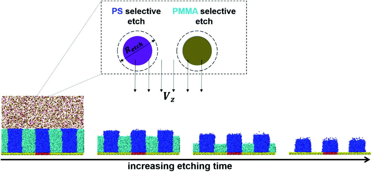 | ||
| Fig. 2 Kinetic evolution of resist morphology with PS-selective and PMMA-selective etch beads. PS-selective beads remove PS beads while PMMA-selective beads remove PMMA. | ||
Etch beads possess high energy and move in a near collisionless state with each other. As the pressures in the system are in the range of tens of mTorr, this assumption of a collisionless state is fair. For interaction between etch beads, a soft cosine potential with a substantially lower energy prefactor ε = 0.05 and a cut-off radius rc = 1.0 is described by eqn (4). The soft potential essentially prevents any etch bead from overlapping while maintaining the collective sheath velocity, Vz.
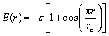 | (4) |
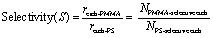
The etching was performed at P = 10 mTorr to maintain an etch bead density of 0.0165 beads per nm3 (refer to the ESI† for etch bead coarse-graining). Etching selectivity is the PMMA etching rate over PS etching rate, calculated viaeqn (5). retch-PMMA is the PMMA etching rate and retch-PS is the PS etching rate, NPMMA-selectiveetch is the number of PMMA-selective etch beads, and NPS-selectiveetch is the number of PS-selective etch beads. It depends on parameters like etch-chemistry and bias voltage source among others. Choosing the appropriate etch-gas with the optimum selectivity requires a thorough investigation of the etching mechanics and post-etch chemistry, which is out of the scope of this study. Selectivities of 1.5, 2, 2.5, and 3.5 were applied in this paper.
 | (5) |
The post-etch morphology is then evaluated for its effective selectivity, resist height, line-width roughness and line-edge roughness in space and frequency domains.
Experimental verification
The experimental trials were performed with the LiNe flow process using the block copolymer PME-7001 on NLD-128 (PS mat pinning) and NLD-127 (neutral brush) prepatterns. The pattern multiplication is 3× with a patterning pitch of 90 nm and a pinning width of 18 nm (optimum for experimental trials). The film thickness is about 1.2L0 ∼ 35 nm to offer higher tolerance for the pattern for post PMMA-etch pattern transfer. Substrate fabrication and annealing conditions have been kept similar to those of Liu et al.12,13 The PMMA phase is etched with Ar/O2 plasma etch with effective selectivity close to 2.5.The PS bead coordinates were analyzed at post-annealing, pre-etching and post-etching stages to obtain each PS domain width, LER and LWR. The lamellar BCP was sliced into 2 nm thick layers along the film thickness. For each layer, the edges of the domains were located. The distance between the corresponding edges is the width of that domain, and three times the standard deviation of this width is the associated line-width roughness of this domain. Similarly, three times the standard deviation of the edge bead coordinates, along a mean straight line for the layer, is the line-edge roughness at that layer height.
Wet-etching was also investigated in this work. Due to its lack of practical relevance, the results are addressed in the ESI.†
III. Results and discussion
Effect of selectivity on post-etch PS domain morphology
As we define the simulation selectivity parameter as the ratio of the number of PMMA-selective etch beads to PS-selective beads, it is important to find the effective selectivity by measuring the post-etch resist heights after complete PMMA removal. As the film thickness is 28 nm, the effective selectivity can be defined as: | (6) |
ht PMMA and htPS are the heights of the two domains at any particular time. The kinetic evolution of the system morphology and the effective selectivity for the morphology for three different selectivities are shown in Fig. 3.
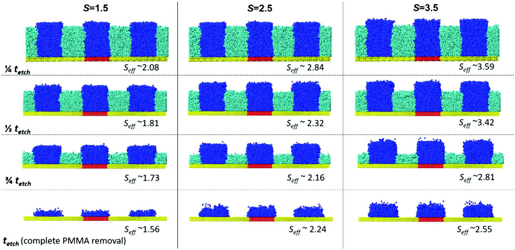 | ||
| Fig. 3 Kinetic evolution of resist profile at constant P = 10 mTorr and Vz = 0.01σ/τ at three different selectivities, S = 1.5, 2.5, and 3.5. The effective selectivity is calculated by measuring the PS and PMMA domain heights. | ||
For the same domain thickness, a higher initial selectivity S leads to taller final resist heights at complete PMMA removal. This is expected as the system has a greater number of PMMA-selective etch beads at the same pressure as compared to PS-selective etch beads. The final effect selectivity, Seff, is lower than the initially defined simulation selectivity parameter S as the ratio of the two types of selective etch beads. The instantaneous Seff also decreases with increasing etch time. For lower etch times, Seff > S, and as time increases, the effective selectivity falls below initial selectivity for S = 2.5 and S = 3.5, while remaining incrementally above initial selectivity for S = 1.5 (Fig. 4).
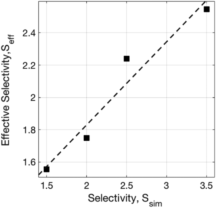 | ||
| Fig. 4 Effective selectivity (Seff) calculated at complete PMMA removal as a function of imposed simulation selectivity (Ssim). | ||
In the etching process, the post-etch PS domain morphology is evaluated at complete PMMA removal. The line-width and the line-edge roughness (Fig. 5) are plotted as a function of the height measured from the bottom substrate.
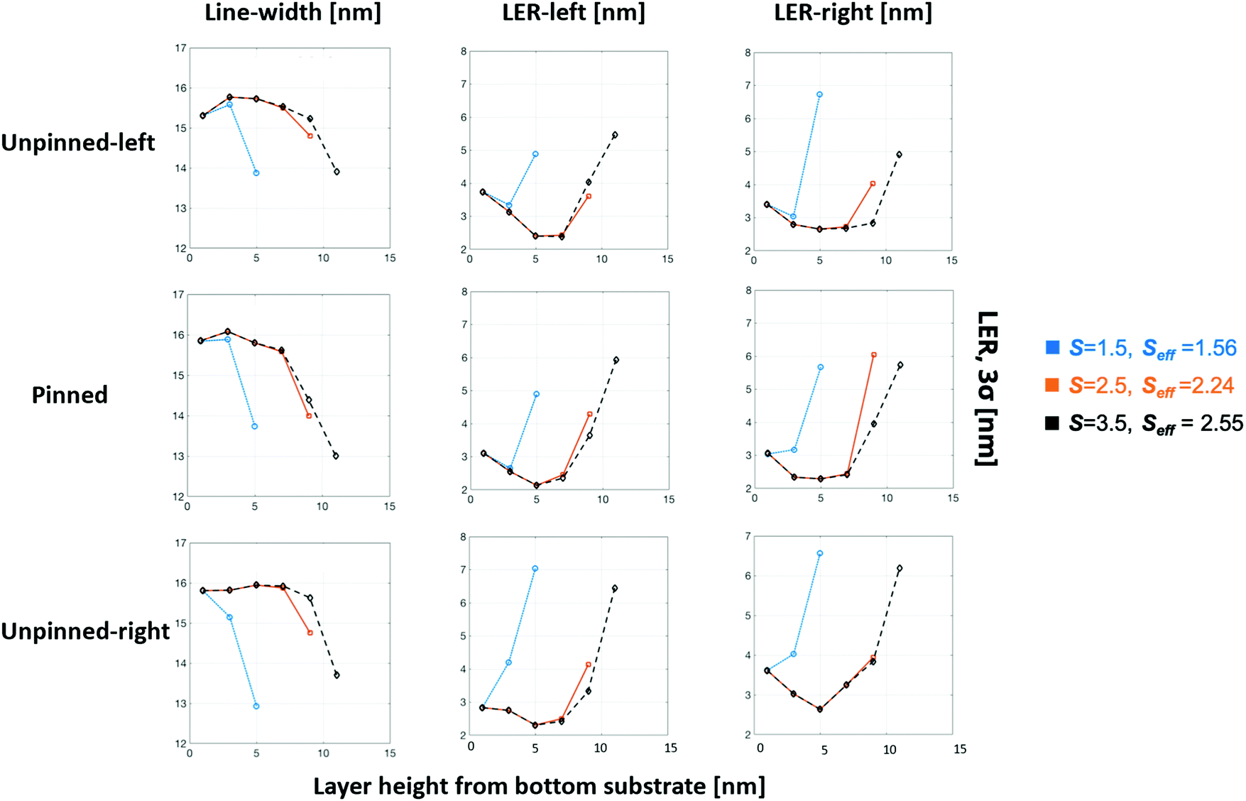 | ||
| Fig. 5 PS line-width (left column), PS domain left edge LER (middle column) and PS domain right edge LER (right column) vs. layer height from the substrate plots for three selectivities. Pinned area is the area on the top of the cross-linking PS substrate. Unpinned-left is the area at the left of the pinned area, and unpinned-right is at the right. | ||
The results show that away from the bottom substrate, close to the PS top surface, the line-width becomes lower, leading to a tapered structure in the resist morphology. The tapered top region is also rougher than the edge layers near the bottom surface. This observation is true for all three selectivities, albeit the lower selectivity has lower PS domain heights. It is also important to note that PS domain morphology of the top part, which has a lower line-width, will not contribute to the subsequent pattern transfers, but the sidewall roughness below the top PS part will strongly affect the silicon pattern transfer. Thus, for the height averaged LER calculation, the top abrasive substrate is not considered. As S = 3.5 leads to a final Seff = 2.55, a selectivity reported for the popular Ar/O2 etch chemistry, we employ S = 3.5 for subsequent multi-stage LER comparisons.
Multi-stage LER evaluation
The three-dimensional morphology and LER were evaluated along the film thickness and at each stage of the process, as shown in Fig. 6. The PS edge for the post-etch stage has a contribution from BCP interfacial width and the etching process while pre-etch edges have a contribution only from BCP interface fluctuations. For the three PS domains, as evident from Fig. 6, the height averaged LER is the highest for the annealing stage. That is because at the elevated temperatures, as the melt has higher kinetic energy, the interface has higher fluctuations. For the different layers, there is a trend that the layers in the middle have lower LER values compared with the top or bottom parts for all three stages. The effect of the guiding force is more predominant close to the bottom substrate while the upper region of the resist experiences less of an effect of the substrate patterning, but it bears the highest impact of incoming etch beads. Thus, the middle layers show lower roughness values on average. Cooling the system below the glass transition temperature (pre-etch stage) lowers the LER. The sidewall roughness post-dry etch leads to an increase in the roughness with a 〈LER〉 = 2.92 nm, but is still lower than the post-annealing LER. This is in contrast with the post-solvent etch 〈LER〉, which is almost the same in magnitude as the pre-etch value (refer ESI†).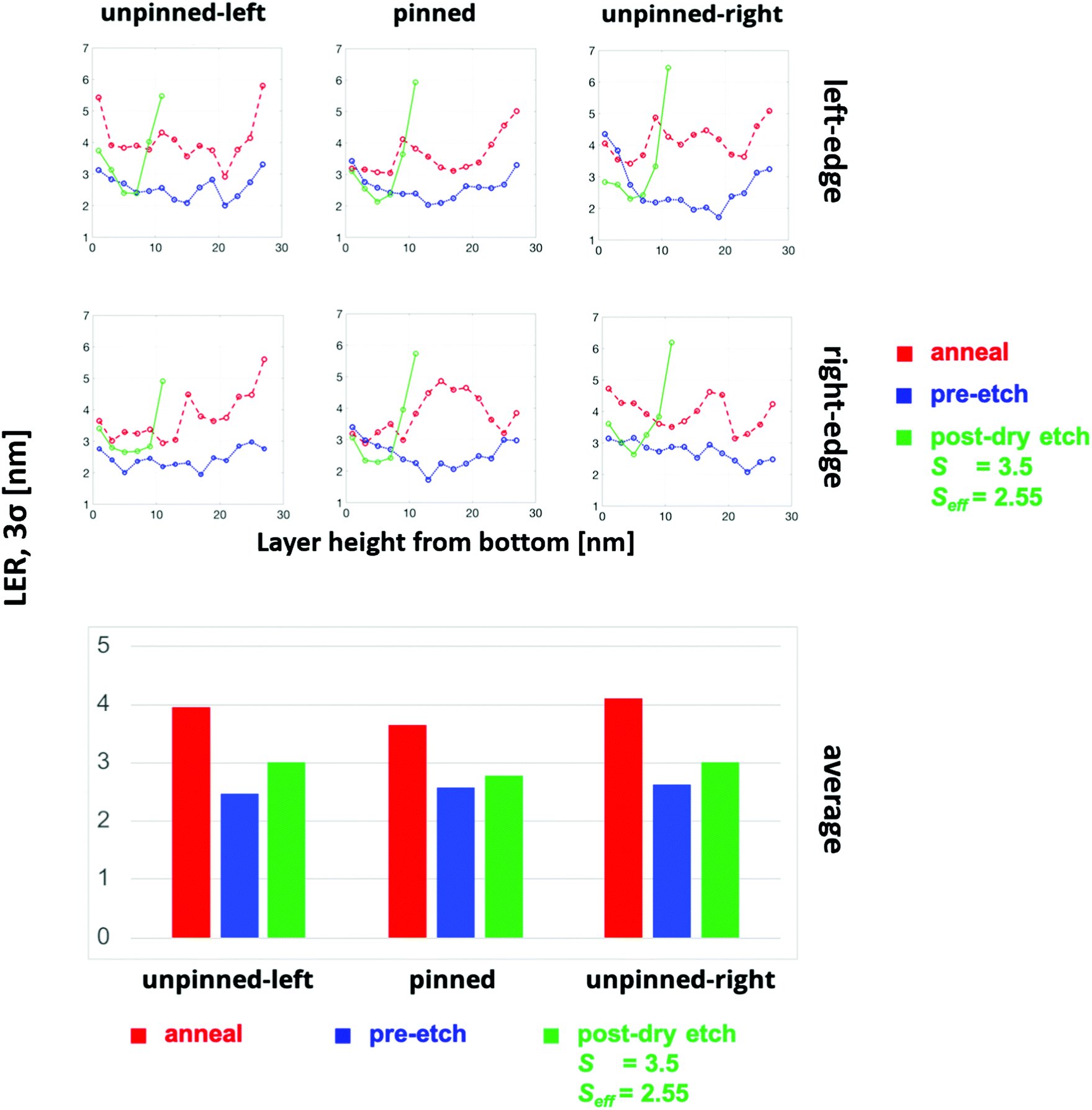 | ||
| Fig. 6 LER vs. film thickness plots (top 2 rows stand for left edge and right edge, respectively) and their average values (third row) for the three process stages: annealing (red), pre-etching (blue) and post-etching (green). | ||
To understand the contributions of the low and high frequency roughness, the power spectral density (PSD) for both edges of the three domains for the planar layers (separated at every 2 nm) was plotted in Fig. 7. The order followed in the space domain holds true in the frequency domain. On average, PSDanneal > PSDpost-etch > PSDpre-etch.
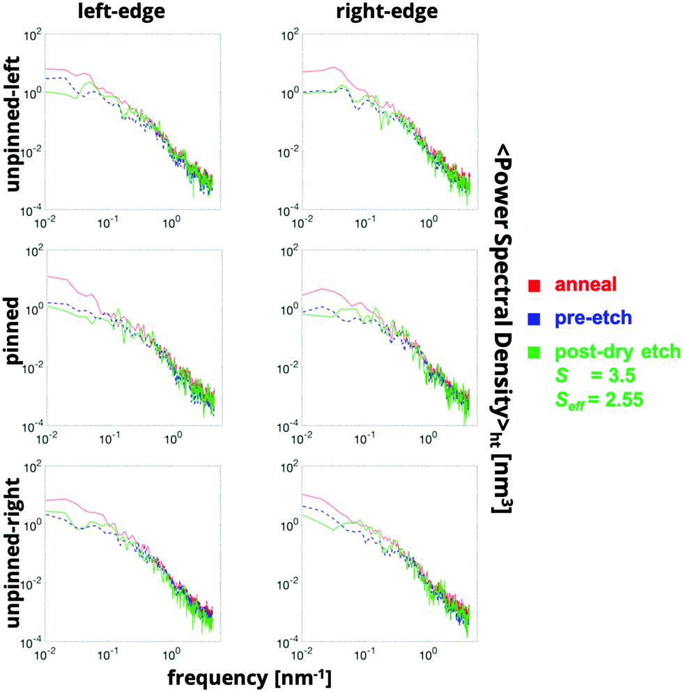 | ||
| Fig. 7 Height averaged power spectral density for PS domains for the three process stages. | ||
For wet-etching simulations, PSD showed a higher contribution for low frequencies for post-solvent etch and a higher contribution for high frequencies for pre-etch morphologies (refer to the ESI†). This observation is not true for the post-dry etch morphology.
Comparison with experimental results
The simulation values were compared to experimental results obtained from a representative SEM image of a self-assembled PS-b-PMMA with L0 ∼ 28 nm. The PMMA phase of the self-assembled BCP was etched off with O2/Ar based plasma. The experimental SEM image corresponds to a pixel size of ∼1.25 nm. The image was processed using Median and Gaussian filters after which the edges were detected using the Canny edge detection algorithm (Fig. 8a).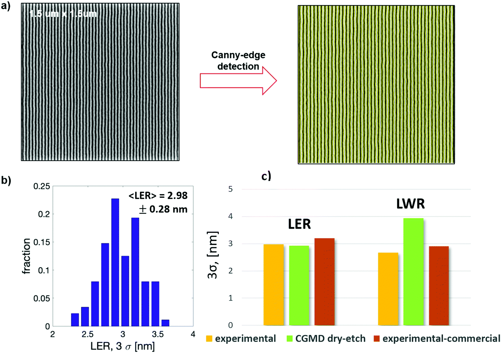 | ||
| Fig. 8 (a) Edge detected SEM image for PMMA etched line space pattern obtained via LiNe flow. (b) Histogram of LER for (a). (c) Comparison between experimental roughness and height averaged CGMD results. Yellow bars are represent the experimental inhouse-image analysis method, green bars represent the simulation, and brown bars represent the commercially used experimental image analysis method. | ||
For the 62 clean lines captured, 〈LER〉exp = 2.98 ± 0.28 nm (Fig. 8b). This is in close agreement with the simulations for the height averaged (every 2 nm) roughness value for the 6 edges, 〈LER〉sim = 2.92 nm. The 〈LWR〉sim = 3.94 nm value predicted from the CGMD simulation shows a slight deviation from the value of the SEM image of 〈LWR〉exp = 2.67 ± 0.16 nm. Although the LWR values are slightly higher, considering the fact that these simulations are coarse-grained with a coarse-graining of 1 nm, under the various assumptions of dry-etching, the sufficiently close agreement is encouraging. To ensure that the image analysis method applied here is accurate, roughness was also evaluated using commercial software, proSEM by Genisys (called experimental-commercial in legend). The SEM image was processed using Gaussian filtering and edges were detected using the Sigmoidal Fit method. 〈LER〉exp-com = 3.20 nm, and 〈LWR〉exp-com = 2.90 nm. The results from the two different experimental image analysis methods are in good agreement, validating the image analysis method and the simulation model.
The deviation in line-edges obtained for each line in the SEM image was treated as a signal in length that was low-pass filtered to remove any spatial aliasing and subsequently windowed using a 4-term Blackman–Harris window to reduce emphasis on the edge points in the series. The cut-off frequency chosen was 0.9 times the Nyquist frequency. The processed signal was then Fourier transformed to generate a surface PSD of the 62 lines, as shown in Fig. 9a. Beyond the correlation frequency, the high frequency contribution was further resolved by fitting a straight line for each of the 62 signals. The slope obtained from this fit denotes the fractal dimension, D (Fig. 9b) with 〈D〉 = 1.77 ± 0.1016. The fractal dimension for a self-similar series can be related to the Hurst or roughness exponent (H) by D = 2 − H, with higher H indicating a less volatile trend. 〈H〉 between 0 and 0.5 in general and 〈H〉 = 0.23 for the current image signify a long-term switching between high and low edge deviations in adjacent pixels lasting for a substantially long length across the line edge.
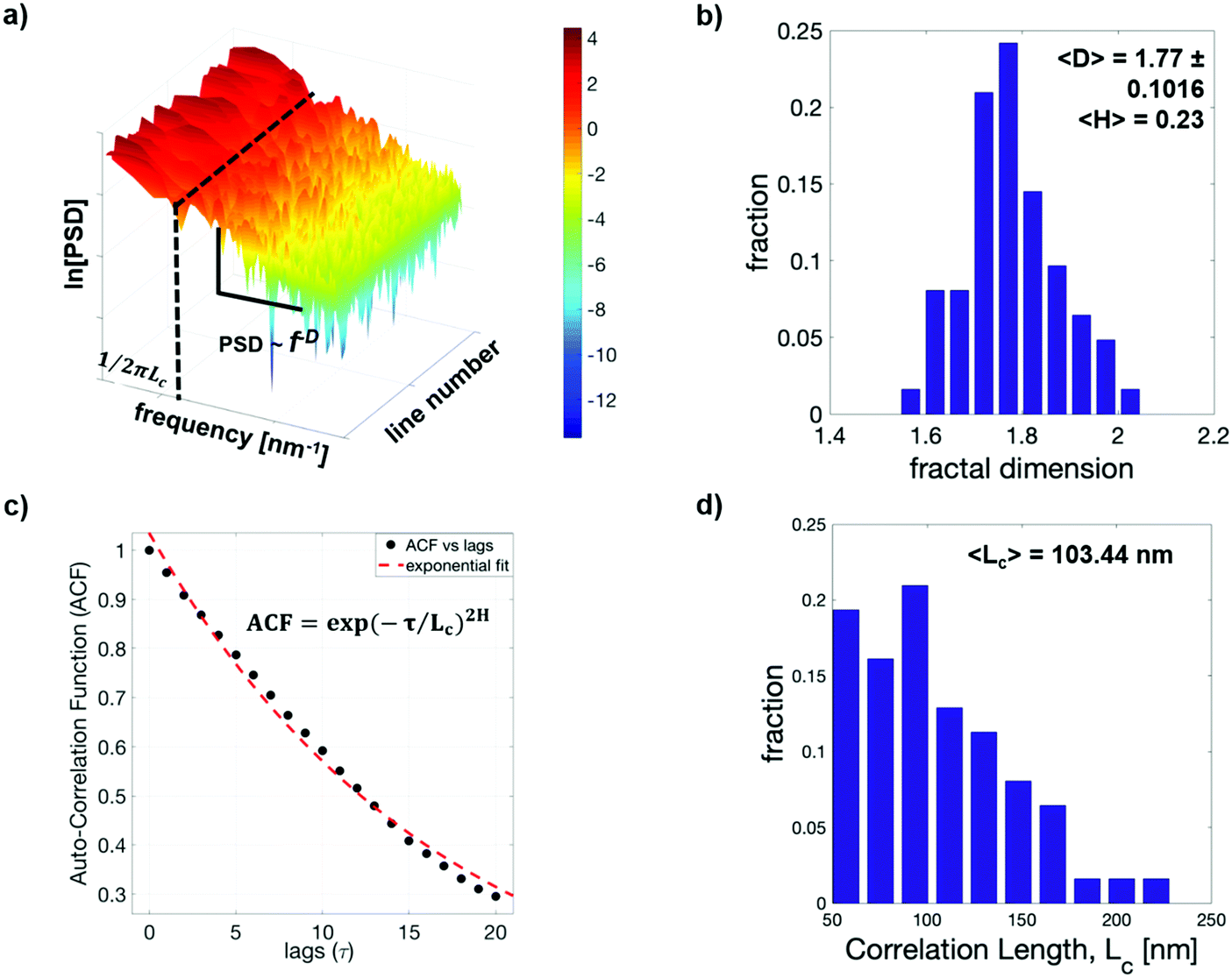 | ||
| Fig. 9 (a) Surface power spectral density example plot. Beyond the correlation length, the PSD is fit to f-D. (b) Fractal dimension histogram for the 62 defect free lines captured through image analysis. (c) Exponential fit for the auto-correlation function for a sample line. The roughness exponent, H, is obtained from (b) for each of the lines. (d) Histogram for correlation length Lc, obtained from fitting the exponential auto-correlation function. | ||
As Fig. 9a shows, the PSD for each of the individual lines is noisy. The exact point of distinction between the low and high frequencies to obtain the correlation length can be tricky using only the PSD curves. Alternatively, the auto-correlation function (ACF) can be generated for each of the lines as a function of the lag (τ). This ACF is fit to an exponential fall model, ACF = exp(−τ/Lc)2H, as in Fig. 9c. The histogram for Lc is shown in Fig. 9d with 〈Lc〉 = 103.44 nm indicating a significant contribution from low frequency roughness. As we are limited with our simulation box size to ∼100 nm line length as opposed to 1500 nm for the experimental line length, comparison in the frequency domains was not made for the two.
Finally, a 3D comparison of the dry etched simulation morphology with a cross-sectional PMMA etched SEM image was carried out. A qualitative comparison can be made between the experimental image in Fig. 10b and a simulation image of similar BCP blends both pre-etch and post-etch using selectivity = 3.5 in Fig. 10a. The cross-sectional image was processed to isolate individual domains and averaged out over the optimally detected PS domains. This edge detected averaged domain and one selected individual domain are compared with the pinned domain and the average of unpinned domains from the simulations. The results show that the experimental SEM image has a similar gradient trend for the line-width as compared to that of the dry-etching (Fig. 10c). This gradient is a closer match for the pinned domain compared to that for the unpinned ones. Both pinned and unpinned areas showed a closer match with that of the selected experimental domain compared to those of the averaged experimental results. One of the reasons for the high averaged gradient in the SEM image could be a higher BCP mass at the bottom substrate. It is likely that the excess mass is caused by incomplete PMMA removal. Similar PS-PMMA phase densities lead to a poor interface distinction for the BCP edge. Correction for this overestimation will lead to a closer agreement. Moreover, in experiments, the film thickness is 35 nm while in simulation, it is 28 nm. A higher thickness may lead to a higher gradient, based on the trend shown in the SEM images.
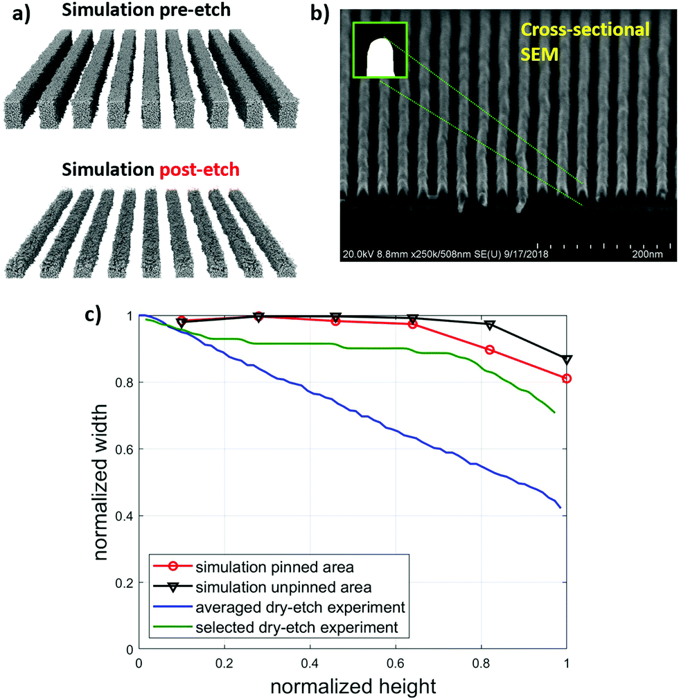 | ||
| Fig. 10 (a) Repeated patterns generated for the dry etched CGMD simulations on flat substrate geometry. (b) Cross-sectional SEM image for PMMA etched-off line and space patterns and one selected domain shape. (c) Remaining PS domain normalized line-width vs. normalized height for simulation pinned and unpinned areas, and experimental averaged and selected areas. | ||
IV. Conclusions
Using a large-scale CGMD model, we have studied the three-dimensional profiles of line and space patterns formed from symmetric BCPs at three process stages: annealing, and pre- and post-dry etching. The etching is studied using a novel modeling approach for a DSA dry-etching schematic. Etch gas selectivities were varied and the kinetic evolution with the instantaneous effective selectivity was assessed. For the optimized selectivity, the PS domain morphology was studied by evaluating the line-width and line edge roughness over the film thickness. Subsequently, a multi-stage roughness evaluation was performed at the annealing, pre-etching and post-etching stages of the process. The roughness magnitude was the highest in the annealing stage followed by post-etching and pre-etching. This observation was also true on average in the frequency domain for both low and high frequencies.Finally, comparison with equivalent Liu–Nealey flow experiments showed a close match in the average roughness values obtained by processing the SEM images and the CGMD results. A similar gradient trend on the remaining PS domain after dry-etching was also observed in both simulation and experiments.
This work has introduced a novel etching simulation methodology in addition to the directed self-assembly of the BCP. Most of the prior DSA work essentially measured the pre-etch BCP interfacial-widths and not the post-etch edge roughness of the polymeric domains. The lower degree of coarse-graining also allows us to capture the high frequency roughness bands. The three-dimensional roughness analysis at various layer heights would give the experimentalist a better roughness estimate compared to an approximated value from SEM images. The reliance on a sophisticated characterization method like STEM tomography for accurate 3D roughness evaluation can also be reduced with from the help of simulations similar to the ones described in this work. For the aforementioned reasons, this simulation model can be used as a time and resource saving tool to investigate and optimize process parameters like substrate dimensions, BCP properties, and etching parameters to form defect-free lamellae with mitigated LER. The model lays a foundation to probe other problems of interest in DSA like the effect of substrate topography on 3D roughness or strategies to mitigate roughness with specific BCP blends.
The results of similar simulations for a topographical substrate will be shown in a subsequent publication. This model can be further improved by accounting for cross-linking of the PS surface upon interaction with the etch-beads and accounting for reactive-ion etching along with ion bombardment for the dry etching mechanism. Replacing the substrate stationary beads with hydroxy terminated PS-PMMA brush beads (the same as in experiments) might be another option to investigate the BCP-DSA and etch processes thoroughly.
Conflicts of interest
There are no conflicts to declare.Acknowledgements
The simulations were performed using the LAMMPS open source software package.40,41 The work was supported by EMD Performance Materials (Cornell OSP NO. 74981). This work used the Extreme Science and Engineering Discovery Environment (XSEDE),42 which is supported by National Science Foundation grant number ACI-1053575.References
- S. J. Jeong, J. Y. Kim, B. H. Kim, H. S. Moon and S. O. Kim, Directed self-assembly of block copolymers for next generation nanolithography, Mater. Today, 2013, 16(12), 468–476 CrossRef CAS.
- C. C. Liu, A. Ramírez-Hernández, E. Han, G. S. Craig, Y. Tada, H. Yoshida, H. Kang, S. Ji, P. Gopalan, J. J. de Pablo and P. F. Nealey, Chemical patterns for directed self-assembly of lamellae-forming block copolymers with density multiplication of features, Macromolecules, 2013, 46(4), 1415–1424 CrossRef CAS.
- R. Ruiz, H. Kang, F. A. Detcheverry, E. Dobisz, D. S. Kercher, T. R. Albrecht, J. J. de Pablo and P. F. Nealey, Density multiplication and improved lithography by directed block copolymer assembly, Science, 2008, 321(5891), 936–939 CrossRef CAS PubMed.
- C. A. Mack, Field guide to optical lithography, SPIE Press, Bellingham, Washington, USA, 2006 Search PubMed.
- B. Wu and A. Kumar, Extreme ultraviolet lithography: a review, J. Vac. Sci. Technol., B: Microelectron. Nanometer Struct.–Process., Meas., Phenom., 2007, 25(6), 1743–1761 CrossRef CAS.
- F. S. Bates and G. H. Fredrickson, Block copolymers—designer soft materials, Phys. Today, 1999, 52(2), 32–38 CrossRef CAS.
- R. A. Segalman, K. E. Schaefer, G. H. Fredrickson, E. J. Kramer and S. Magonov, Topographic templating of islands and holes in highly asymmetric block copolymer films, Macromolecules, 2003, 36(12), 4498–4506 CrossRef CAS.
- K. G. AT, K. W. Gotrik, A. F. Hannon, A. Alexander-Katz, C. A. Ross and K. K. Berggren, Templating three-dimensional self-assembled structures in bilayer block copolymer films, Science, 2012, 336(6086), 1294–1298 CrossRef PubMed.
- S. Pinge, G. Lin, D. Baskaran, M. Padmanaban and Y. L. Joo, Designing an ordered template of cylindrical arrays based on a simple flat plate confinement of block copolymers: A coarse-grained molecular dynamics study, Soft Matter, 2018, 14(4), 597–613 RSC.
- J. Y. Cheng, C. T. Rettner, D. P. Sanders, H. C. Kim and W. D. Hinsberg, Dense self-assembly on sparse chemical patterns: Rectifying and multiplying lithographic patterns using block copolymers, Adv. Mater., 2008, 20(16), 3155–3158 CrossRef CAS.
- S. O. Kim, H. H. Solak, M. P. Stoykovich, N. J. Ferrier, J. J. de Pablo and P. F. Nealey, Epitaxial self-assembly of block copolymers on lithographically defined nanopatterned substrates, Nature, 2003, 424(6947), 411–414 CrossRef CAS PubMed.
- C. C. Liu, E. Han, M. S. Onses, C. J. Thode, S. Ji, P. Gopalan and P. F. Nealey, Fabrication of lithographically defined chemically patterned polymer brushes and mats, Macromolecules, 2011, 44(7), 1876–1885 CrossRef CAS.
- C. C. Liu, A. Ramírez-Hernández, E. Han, G. S. Craig, Y. Tada, H. Yoshida, H. Kang, S. Ji, P. Gopalan, J. J. de Pablo and P. F. Nealey, Chemical patterns for directed self-assembly of lamellae-forming block copolymers with density multiplication of features, Macromolecules, 2013, 46(4), 1415–1424 CrossRef CAS.
- C. C. Liu, P. F. Nealey, Y. H. Ting and A. E. Wendt, Pattern transfer using poly (styrene-block-methyl methacrylate) copolymer films and reactive ion etching, J. Vac. Sci. Technol., B: Microelectron. Nanometer Struct.–Process., Meas., Phenom., 2007, 25(6), 1963–1968 CrossRef CAS.
- M. Muramatsu, M. Iwashita, T. Kitano, T. Toshima, M. Somervell, Y. Seino, D. Kawamura, M. Kanno, K. Kobayashi and T. Azuma, Nanopatterning of diblock copolymer directed self-assembly lithography with wet development, J. Micro/Nanolithogr., MEMS, MOEMS, 2012, 11(3), 031305 CrossRef.
- C. T. Black, K. W. Guarini, K. R. Milkove, S. M. Baker, T. P. Russell and M. T. Tuominen, Integration of self-assembled diblock copolymers for semiconductor capacitor fabrication, Appl. Phys. Lett., 2001, 79(3), 409–411 CrossRef CAS.
- A. Gharbi, R. Tiron, P. Pimenta Barros, M. Argoud, I. Servin, X. Chevalier, C. Nicolet and C. Navarro, PMMA removal options by wet development in PS-b-PMMA block copolymer for nanolithographic mask fabrication, J. Vac. Sci. Technol., B: Nanotechnol. Microelectron.: Mater., Process., Meas., Phenom., 2015, 33(5), 051602 Search PubMed.
- T. Y. Chung, D. Nest, D. B. Graves, F. Weilnboeck, R. L. Bruce, G. S. Oehrlein, D. Wang, M. Li and E. A. Hudson, Electron, ion and vacuum ultraviolet photon effects in 193 nm photoresist surface roughening, J. Phys. D: Appl. Phys., 2010, 43(27), 272001 CrossRef.
- D. Nest, T. Y. Chung, J. J. Vegh, D. B. Graves, R. L. Bruce, T. Lin, R. J. Phaneuf, G. S. Oehrlein, B. K. Long and C. G. Willson, Role of polymer structure and ceiling temperature in polymer roughening and degradation during plasma processing: a beam system study of P4MS and PαMS, J. Phys. D: Appl. Phys., 2010, 43(8), 085204 CrossRef.
- Y. H. Ting, C. C. Liu, S. M. Park, H. Jiang, P. F. Nealey and A. E. Wendt, Surface roughening of polystyrene and poly (methyl methacrylate) in Ar/O2 plasma etching, Polymers, 2010, 2(4), 649–663 CrossRef CAS.
- J. Zekonyte, V. Zaporojtchenko and F. Faupel, Investigation of the drastic change in the sputter rate of polymers at low ion fluence, Nucl. Instrum. Methods Phys. Res., Sect. B, 2005, 236(1–4), 241–248 CrossRef CAS.
- V. Zaporojtchenko, J. Zekonyte and F. Faupel, Effects of ion beam treatment on atomic and macroscopic adhesion of copper to different polymer materials, Nucl. Instrum. Methods Phys. Res., Sect. B, 2007, 265(1), 139–145 CrossRef CAS.
- M. Sumiya, R. Bruce, S. Engelmann, F. Weilnboeck and G. S. Oehrlein, Study of 193 nm photoresist degradation during short time fluorocarbon plasma exposure. I. Studies of modified layer formation, J. Vac. Sci. Technol., B: Microelectron. Nanometer Struct.–Process., Meas., Phenom., 2008, 26(5), 1637–1646 CrossRef CAS.
- M. Sumiya, R. Bruce, S. Engelmann, F. Weilnboeck and G. S. Oehrlein, Study of 193 nm photoresist degradation during short time fluorocarbon plasma exposures. II. Plasma parameter trends for photoresist degradation, J. Vac. Sci. Technol., B: Microelectron. Nanometer Struct.–Process., Meas., Phenom., 2008, 26(5), 1647–1653 CrossRef CAS.
- E. Baravelli, A. Dixit, R. Rooyackers, M. Jurczak, N. Speciale and K. De Meyer, Impact of line-edge roughness on FinFET matching performance, IEEE Trans. Electron Devices, 2007, 54(9), 2466–2474 Search PubMed.
- G. Leung, L. Lai, P. Gupta and C. O. Chui, Device-and circuit-level variability caused by line edge roughness for sub-32-nm FinFET technologies, IEEE Trans. Electron Devices, 2012, 59(8), 2057–2063 Search PubMed.
- A. W. Bosse, E. K. Lin, R. L. Jones and A. Karim, Interfacial fluctuations in an ideal block copolymer resist, Soft Matter, 2009, 5(21), 4266–4271 RSC.
- M. W. Matsen and F. S. Bates, Unifying weak-and strong-segregation block copolymer theories, Macromolecules, 1996, 29(4), 1091–1098 CrossRef CAS.
- F. A. Detcheverry, D. Q. Pike, U. Nagpal, P. F. Nealey and J. J. de Pablo, Theoretically informed coarse grain simulations of block copolymer melts: method and applications, Soft Matter, 2009, 5(24), 4858–4865 RSC.
- S. M. Hur, V. Thapar, A. Ramírez-Hernández, G. Khaira, T. Segal-Peretz, P. A. Rincon-Delgadillo, W. Li, M. Müller, P. F. Nealey and J. J. de Pablo, Molecular pathways for defect annihilation in directed self-assembly, Proc. Natl. Acad. Sci. U. S. A., 2015, 112(46), 14144 CrossRef CAS PubMed.
- S. M. Hur, G. S. Khaira, A. Ramírez-Hernández, M. Müller, P. F. Nealey and J. J. de Pablo, Simulation of defect reduction in block copolymer thin films by solvent annealing, ACS Macro Lett., 2014, 4(1), 11–15 CrossRef.
- K. C. Daoulas, M. Müller, M. P. Stoykovich, H. Kang, J. J. de Pablo and P. F. Nealey, Directed copolymer assembly on chemical substrate patterns: A phenomenological and single-chain-in-mean-field simulations study of the influence of roughness in the substrate pattern, Langmuir, 2008, 24(4), 1284–1295 CrossRef CAS.
- M. P. Stoykovich, K. C. Daoulas, M. Müller, H. Kang, J. J. de Pablo and P. F. Nealey, Remediation of line edge roughness in chemical nanopatterns by the directed assembly of overlying block copolymer films, Macromolecules, 2010, 43(5), 2334–2342 CrossRef CAS.
- T. Segal-Peretz, J. Ren, S. Xiong, G. Khaira, A. Bowen, L. E. Ocola, R. Divan, M. Doxastakis, N. J. Ferrier, J. de Pablo and P. F. Nealey, Quantitative three-dimensional characterization of block copolymer directed self-assembly on combined chemical and topographical prepatterned templates, ACS Nano, 2017, 11(2), 1307–1319 CrossRef CAS PubMed.
- A. J. Peters, R. A. Lawson, P. J. Ludovice and C. L. Henderson, Detailed molecular dynamics studies of block copolymer directed self-assembly: Effect of guiding layer properties, J. Vac. Sci. Technol., B: Nanotechnol. Microelectron.: Mater., Process., Meas., Phenom., 2013, 31(6), 06F302 Search PubMed.
- A. J. Peters, R. A. Lawson, P. J. Ludovice and C. L. Henderson, Effects of block copolymer polydispersity and χN on pattern line edge roughness and line width roughness from directed self-assembly of diblock copolymers, Proc. SPIE, 2013, 8680, 868020 CrossRef.
- H. Morita, K. Tanaka, T. Kajiyama, T. Nishi and M. Doi, Study of the glass transition temperature of polymer surface by coarse-grained molecular dynamics simulation, Macromolecules, 2006, 39(18), 6233–6237 CrossRef CAS.
- K. Kremer and G. S. Grest, Dynamics of entangled linear polymer melts: A molecular-dynamics simulation, J. Chem. Phys., 1990, 92(8), 5057–5086 CrossRef CAS.
- J. D. Weeks, D. Chandler and H. C. Andersen, Role of repulsive forces in determining the equilibrium structure of simple liquids, J. Chem. Phys., 1971, 54(12), 5237–5247 CrossRef CAS.
- P. J. In't Veld, S. J. Plimpton and G. S. Grest, Accurate and efficient methods for modeling colloidal mixtures in an explicit solvent using molecular dynamics, Comput. Phys. Commun., 2008, 179(5), 320–329 CrossRef.
- S. Plimpton, Fast parallel algorithms for short-range molecular dynamics, J. Comput. Phys., 1995, 117(1), 1–9 CrossRef CAS.
- J. Towns, T. Cockerill, M. Dahan, I. Foster, K. Gaither, A. Grimshaw, V. Hazlewood, S. Lathrop, D. Lifka, G. D. Peterson and R. Roskies, XSEDE: accelerating scientific discovery, Comput. Sci. Eng., 2014, 16(5), 62–74 Search PubMed.
Footnote |
| † Electronic supplementary information (ESI) available. See DOI: 10.1039/c9cp05398k |
| This journal is © the Owner Societies 2020 |