DOI:
10.1039/D0CE01344G
(Paper)
CrystEngComm, 2020,
22, 8299-8312
Correlation between structural properties and nonradiative recombination behaviors of threading dislocations in freestanding GaN substrates grown by hydride vapor phase epitaxy†
Received
15th September 2020
, Accepted 22nd October 2020
First published on 27th October 2020
Abstract
Correlations between the structural properties and nonradiative recombination (NRR) behaviors of threading dislocations in freestanding hydride-vapor-phase-epitaxy (HVPE) GaN substrates were investigated using cathodoluminescence (CL), the etch pit method, transmission electron microscopy (TEM), and multiple-photon excitation photoluminescence (MPPL). A statistical analysis with a one-to-one comparison of 480 CL dark spots (prior to etching) with their corresponding etch pits shows that all dislocation types act as NRR centers with a strong correlation between the NRR rate at the dislocation cores and the pit size. Further TEM observations accurately determined the magnitude and direction of Burgers vectors for dislocations under each type of etch pit, which firmly links the NRR behaviors with the dislocation type. It is found that a dislocation pair composed of (a + c) and (−a + c) threading mixed-type dislocations (TMDs) is the strongest NRR center among the considered dislocation types. The pair runs along the c-axis with a stable distance of 42 nm between them. This is followed by other types of TMD pairs, a + c TMDs, ma + nc TMDs (m and n are integers, m > 1 or n > 1), 1c threading screw dislocations, and 1a threading edge dislocations in descending order of NRR rates. Three-dimensional (3D) dislocation images visualized by MPPL revealed that most of the dislocations are nearly parallel to the c-axis, while the a + c TMDs are susceptible to large tilting. MPPL also indicates that the ma + nc TMDs may result from several merging dislocations.
1. Introduction
GaN is a semiconductor with excellent physical properties that benefits from its wide direct bandgap, high breakdown field, high electron mobility, and high thermal conductivity. GaN has a wide range of applications in both optical devices, such as light-emitting diodes (LEDs) and laser diodes (LDs),1 and electronic devices, such as high-voltage and high-frequency power switches.2 To fully exploit the physical properties of GaN in such devices, there have been numerous efforts in recent years to develop high-quality and large-diameter freestanding GaN (FS-GaN) substrates, on which homoepitaxial growth of GaN layers with a low threading dislocation (TD) density and a precisely controlled carrier concentration can occur. Some promising growth methods for FS-GaN include hydride vapor phase epitaxy (HVPE),3–5 ammonothermal growth,6,7 and the Na-flux method.8
Dislocations are a major type of crystallographic defect in GaN and are generally classified into basal plane dislocations (BPDs) within the {0001} planes or TDs that propagate approximately along the 〈0001〉 direction. The TDs can be further categorized into threading edge-type (TED, b = ma, a = (1/3)〈11![[2 with combining macron]](https://www.rsc.org/images/entities/char_0032_0304.gif) 0〉, m = 1, 2, 3…), screw-type (TSD, b = nc, c = 〈0001〉, n = 1, 2, 3…), and mixed-type (TMD, b = ma + nc) dislocations based on their Burgers vectors (b). In each category, dislocations with an elementary Burgers vector (m = 1 and n = 1) are dominant compared to those with larger Burgers vectors. Henceforth, we refer to the 1a, 1c, and a + c dislocations as TED, TSD, and TMD, respectively, unless specified otherwise. The TDs have deleterious effects on the performance and lifetime of GaN-based devices through mechanisms such as carrier scattering,9,10 carrier trapping via nonradiative recombination (NRR),11–16 and paths for leakage current.17–22 These different mechanisms are connected by the fact that dislocations act as one-dimensional (1D) charged defects that introduce electronic states into the energy gap.14,22–24 It is well accepted that the negative effects of dislocations on devices are strongly dependent on their Burgers vector and are susceptible to other dislocation characteristics, such as their line direction,20 core structure,20,22,25–27 impurity gettering,14,22 and surface morphology.21 However, there are large discrepancies in the literature regarding the relationship between the dislocation behavior and their structural properties. Some authors found that dislocations with the c component (TSDs and TMDs) act as NRR centers, whereas the pure TEDs do not.28,29 Others found that the dislocations with the a component (TEDs and TMDs) act as NRR centers,12,14 whereas the pure TSDs are inactive.14 On the other hand, in terms of leakage current pathways, most groups seem to agree that TSDs, especially those with an open-core, are responsible for the large leakage current under a reverse bias in Schottky barrier diodes (SBDs)30 and vertical PN diodes,18,20,22 even though the types of impurities that accumulate at the dislocations are different. When a Na-flux GaN substrate is used, the leakage current is strongly dependent on the growth sector at the initial stage of the Na-flux growth and has a positive correlation with the magnitude of the Burgers vectors, while the effects of oxygen impurities are implied.21,31
0〉, m = 1, 2, 3…), screw-type (TSD, b = nc, c = 〈0001〉, n = 1, 2, 3…), and mixed-type (TMD, b = ma + nc) dislocations based on their Burgers vectors (b). In each category, dislocations with an elementary Burgers vector (m = 1 and n = 1) are dominant compared to those with larger Burgers vectors. Henceforth, we refer to the 1a, 1c, and a + c dislocations as TED, TSD, and TMD, respectively, unless specified otherwise. The TDs have deleterious effects on the performance and lifetime of GaN-based devices through mechanisms such as carrier scattering,9,10 carrier trapping via nonradiative recombination (NRR),11–16 and paths for leakage current.17–22 These different mechanisms are connected by the fact that dislocations act as one-dimensional (1D) charged defects that introduce electronic states into the energy gap.14,22–24 It is well accepted that the negative effects of dislocations on devices are strongly dependent on their Burgers vector and are susceptible to other dislocation characteristics, such as their line direction,20 core structure,20,22,25–27 impurity gettering,14,22 and surface morphology.21 However, there are large discrepancies in the literature regarding the relationship between the dislocation behavior and their structural properties. Some authors found that dislocations with the c component (TSDs and TMDs) act as NRR centers, whereas the pure TEDs do not.28,29 Others found that the dislocations with the a component (TEDs and TMDs) act as NRR centers,12,14 whereas the pure TSDs are inactive.14 On the other hand, in terms of leakage current pathways, most groups seem to agree that TSDs, especially those with an open-core, are responsible for the large leakage current under a reverse bias in Schottky barrier diodes (SBDs)30 and vertical PN diodes,18,20,22 even though the types of impurities that accumulate at the dislocations are different. When a Na-flux GaN substrate is used, the leakage current is strongly dependent on the growth sector at the initial stage of the Na-flux growth and has a positive correlation with the magnitude of the Burgers vectors, while the effects of oxygen impurities are implied.21,31
There is a lack of consensus on the optical and electrical properties of dislocations in GaN and their relationships with the associated structural properties. This hinders the development of high-quality crystals suitable for fabricating high-performance GaN devices. In this study, we performed a systematic investigation of the correlation between the structural properties and NRR behaviors of TDs. Our study differentiates itself from former studies in the following ways. (1) A 700 μm-thick 2 inch FS-GaN substrate grown by HVPE is investigated, which is the only growth method that has been commercialized for the mass production of GaN substrates. Therefore, the results could be valuable to the device community. (2) The relatively low TD density (around 1 × 107 cm−2) in the sample, compared to that in early heteroepitaxial GaN films grown on foreign substrates like sapphire or SiC,13,15,24,28 allows evaluating the NRR behaviors of individual dislocations. This is because the average spacing between adjacent dislocations is much larger than the carrier diffusion length. The HVPE-GaN is also superior to GaN substrates grown via the ammonothermal method or Na-flux method in terms of lower impurity concentrations. This allows focusing on the structure-related dislocation properties with minimized effects from impurities. (3) In the literature, an optoelectrical property of dislocations is typically correlated to a specific Burgers vector based on matching the TD density as estimated by techniques such as X-ray diffraction (XRD)32,33 or based on a limited number of dislocations observed via transmission electron microscopy (TEM).11,12,15 Here, we conducted one-to-one comparisons of dislocation types and their NRR behaviors for a significant amount (on the order of 103) of dislocations to acquire statistically meaningful results.
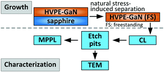
2. Experimental
Fig. 1 shows the growth and characterization processes in this study. A brief description is summarized in Table 1.
 |
| | Fig. 1 A flowchart of the growth and characterization processes. HVPE: hydride vapor phase epitaxy; CL: cathodoluminescence; TEM: transmission electron microscopy; and MPPL: multi-photon excitation photoluminescence. | |
Table 1 Characterization conditions and information obtained
| Characterization |
Conditions |
Information obtained |
| CL |
V
acc = 3 kV, Iems = 1 nA, Re = 93 nm, position-dependent spectra, panchromatic mapping |
Carrier recombination |
| Etch pit method |
Molten KOH + Na2O2, 510 °C, 6 min |
Dislocation position and type |
| TEM |
g
/3g weak beam, large-angle convergent-beam electron diffraction |
Burgers vector, dislocation line |
| MPPL |
Ex. λ = 700 nm, fs pulse, 358–394 nm BPF for detection |
Dislocation 3D visualization |
2.1 FS-GaN substrates prepared with HVPE
The HVPE growth was performed on a commercially available 2 inch c-plane GaN epiwafer as-grown on a sapphire substrate. The growth conditions were similar to those reported previously.3 After the growth of a thick layer (typically >700 μm), a cooling process at a rate of −20 °C min−1 was applied to achieve natural stress-induced separation of the GaN layer from the sapphire substrate and obtain the FS-GaN substrate with a high crystallinity as indicated from XRD measurements. The full-widths at half maximum (FWHMs) of the 0006 and 1![[1 with combining macron]](https://www.rsc.org/images/entities/char_0031_0304.gif) 05 ω-rocking curves were 33 and 25 arcsec, respectively. The TD density decreased with the HVPE growth thickness from a low 108 cm−2 at the initial growth stage to approximately 1 × 107 cm−2 for the last 100 μm. Atomic force microscopy (AFM) measurements showed that the as-grown surface was covered with atomic steps, which indicates a two-dimensional (2D) step-flow growth. The HVPE-grown layer was nominally undoped, and the impurity concentrations as measured from secondary ion mass spectrometry (SIMS) were [C] = 2 × 1016 cm−3, [O] = 3 × 1016 cm−3, and [Si] = 5 × 1015 cm−3.
05 ω-rocking curves were 33 and 25 arcsec, respectively. The TD density decreased with the HVPE growth thickness from a low 108 cm−2 at the initial growth stage to approximately 1 × 107 cm−2 for the last 100 μm. Atomic force microscopy (AFM) measurements showed that the as-grown surface was covered with atomic steps, which indicates a two-dimensional (2D) step-flow growth. The HVPE-grown layer was nominally undoped, and the impurity concentrations as measured from secondary ion mass spectrometry (SIMS) were [C] = 2 × 1016 cm−3, [O] = 3 × 1016 cm−3, and [Si] = 5 × 1015 cm−3.
2.2 Cathodoluminescence (CL) measurements
The characterization began with nondestructive cathodoluminescence (CL) measurements. The CL spectra and mapping were generated from the as-grown GaN surface at room temperature in an SEM (JSM-7800) equipped with a Gatan CL system. The accelerating voltage and beam probe current were 3 kV and 1 nA, respectively. The penetration depth of the electron beam was estimated at approximately 93 nm using the Kanaya–Okayama model.34 The position-dependent CL spectra were collected at each probing point while scanning the entire field-of-view. This allowed evaluating whether there were dislocation-related peak shifts in the CL spectra. The results show that all dislocations acted as NRR centers, which decreased the CL intensity without emitting light at other wavelengths. Therefore, panchromatic CL mappings were used because of their improved image quality.
2.3 Etch pit formation
Chemical etching was performed by dipping the GaN substrate into a 510 °C molten KOH solution with a Na2O2 additive for approximately 6 min. Na2O2 was used as a strong oxidizer to enhance the selective etching and form well-defined pits.35,36 Etch pits formed on the (0001) Ga-face revealed the positions and types of dislocations. The etched thickness in a dislocation-free area was around 300 nm due to isotropic etching along the c-axis. Therefore, the etch pit method probed a slightly deeper region than the CL measurements but did not affect the validity of the TD analysis.
2.4 TEM observations
A focused ion beam (FIB) was used to lift-out dislocation segments beneath the etch pits of interest. Cross-sectional TEM specimens (approximately 150 nm in thickness) were observed using a JEOL JEM-2010DM at 200 kV with a point resolution of 0.196 nm. The g/3g weak-beam dark-field (WBDF) observations37 evaluated whether the dislocations had a- and/or c-components using the g·b invisibility criterion,38 which was followed by an accurate determination of the Burgers vector including both its direction and magnitude using large-angle convergent-beam electron diffraction (LACBED) observations.39–42
2.5 Multi-photon excitation photoluminescence (MPPL)
Three-dimensional (3D) dislocation visualization was performed using a multi-photon excitation photoluminescence (MPPL, Nikon A1 MP+) system. The sample was excited using a Ti–sapphire femtosecond pulsed laser in a scanning mode similar to the CL measurements. The excitation wavelength was λex = 700 nm (Eex = 1.77 eV > Eg/2, 2PPL mode) and the near-band-edge (NBE) emission was collected to generate images using a photomultiplier tube through a 358–394 nm band-pass filter (BPF). As the energy of the incident photons was much lower than the GaN bandgap, strong multi-photon absorption occurred only in a highly localized volume near the focal point of the laser beam. This allowed imaging dislocations in a deeper region by moving the focal point further inside the material without suffering from serious absorption by the surface layer. The 3D image was then reconstructed using a series of MPPL image slices along the depth (Z-direction). It is noted that etch pits at the surface had little influence on the MPPL images of deeper regions.
3. Results and discussion
3.1 CL mapping and etch pits – NRR behavior of dislocations
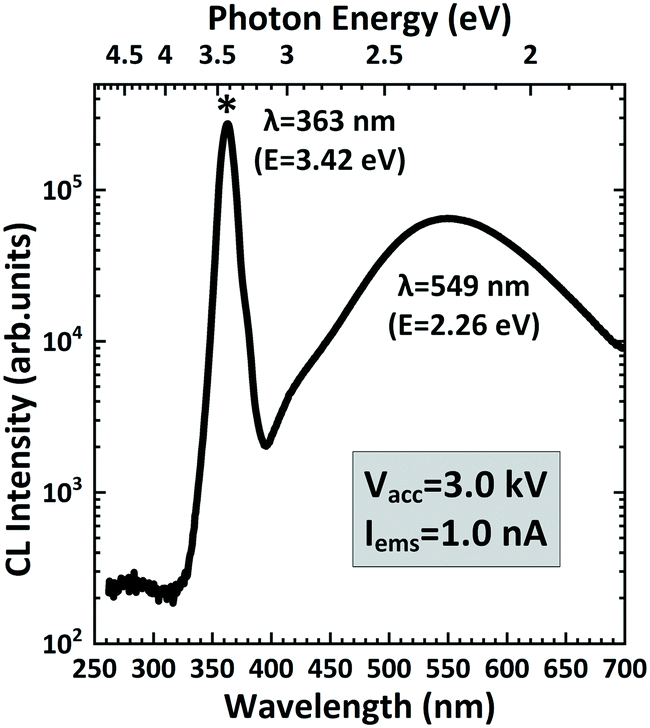
Fig. 2 shows a typical CL spectrum taken from a dislocation-free region. The accelerating voltage was set to 3 kV as a trade-off between the CL image quality and the need to suppress surface recombination.12,13,15,43 The spectrum has a strong NBE emission peak at λ = 363 nm (E = 3.42 eV) and a broad defect-related yellow band with a peak at λ = 549 nm (E = 2.26 eV). The position-dependent CL spectra indicate that all dislocations act as NRR centers, which reduces the intensity of both the NBE and yellow band peaks, though the extent of reduction depends on the dislocation types, as explained later.
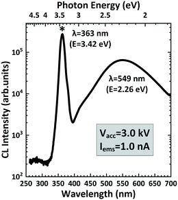 |
| | Fig. 2 A typical CL spectrum taken at an accelerating voltage (Vacc) of 3.0 kV with a probe current (Iems) of approximately 1.0 nA. | |
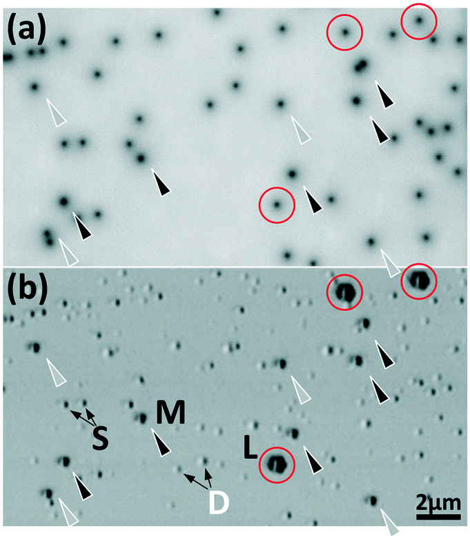
Fig. 3 shows the panchromatic CL and etch pit images taken from the same area. The TDs are revealed as hexagonal etch pits, which presumably formed at the surface outcrops of dislocations. These pits have several discrete size levels denoted as L (large), M (medium), and S (small) in Fig. 3(b). Each size level has a characteristic slope of the six {10n} facets, which results in different pit contrasts under an optical microscope (OM). Besides the hexagonal pits, small shallow dents without a pit core are observed, which are denoted as D in Fig. 3(b). These dents are caused by anisotropic chemical etching processes as initialized by some surface imperfections of the as-grown sample, and there are no dislocations under them, as confirmed by TEM observations (ESI† Fig. S1). There is no formed dent if the substrate surface is polished before chemical etching. Henceforth, the dents are excluded from the etch pits.
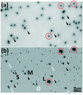 |
| | Fig. 3 (a) Panchromatic CL image and (b) optical image of etch pits taken from the same sample area. The red circles indicate large etch pits (L), while the black and gray triangular marks indicate middle etch pits (M) that correspond to CL dark spots with relatively strong and weak contrast, respectively. S: small etch pits; and D: dent. | |
Comparing the two images in Fig. 3 shows that all pits have a corresponding dark spot in the CL image, suggesting the NRR characteristics of a dislocation. Further investigations indicate a correlation between the pit size and the contrast of the dark spots. The dark spots with the strongest contrast always correspond to M-pits, as marked by black arrows in Fig. 3. It is noted that not all M-pits have the same strong contrast; some (marked as gray arrows in Fig. 3) show similar contrasts to those of the L- and S-pits. This indicates that there must be a certain property of the dislocations that determines both the pit size and dark spot contrast. Different spot contrasts within the same M-group suggest that there are at least two different dislocation types that are revealed as M-pits after chemical etching.
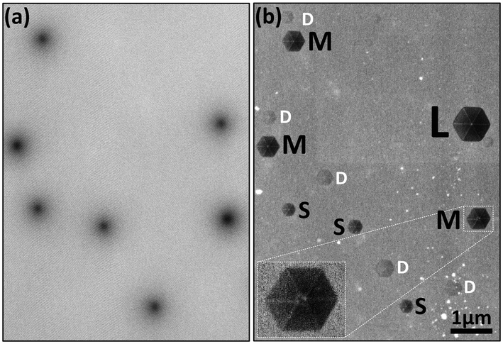
To compare the etch pits with the dark spots in more detail, SEM images were taken from an area containing all etch pit types (Fig. 4). It is unexpected that the M-pit corresponding to the darkest spot had a double-pit-core structure, indicating there may be a dislocation pair underneath. This type of pit is referred to as 2C-M-pit. In comparison, an M-pit that has only a single pit core is referred to as 1C-M-pit. The distance between the two cores is less than 100 nm, which is not recognizable under an OM. There was no double-core structure found for the S- and L- pits, and all S-pits had similarly weak CL contrasts, which is close to that of L-pits. Within the 1C-M-pit category, there is an apparent variation in contrast even though the pit shapes are seemingly identical.
 |
| | Fig. 4 (a) Panchromatic CL image and (b) secondary electron image taken from the same sample area containing representative etch pits from each size level. L: large; M: middle; S: small; D: dent. The inset in (b) shows an enlarged image of an M-pit with double pit cores (a 2C-M-pit). | |
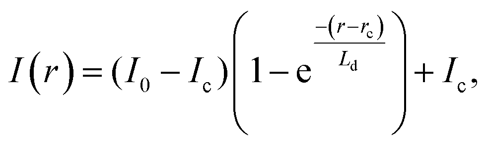
To quantitatively analyze the NRR behavior of dislocations and their correlations with pit size, we carried out fitting for 480 CL dark spots. We assumed the following. (1) The TDs are 1D carrier sinks parallel to the c-axis,13 which is valid because of the small penetration depth of the electron beam. (2) The NRR occurs in a cylinder region centered at the TD core.44 (3) The TD cores have a dimension (rc) approximately equal to the lattice constant a. (4) The carrier diffusion coefficient is isotropic in the {0001} plane. The 2D steady-state diffusion equations lead to a CL intensity profile, I(r), of the following form:
| |  | (1) |
where
r is the distance from the TD core,
I0 is the CL intensity at the dislocation-free position,
Ld is the carrier diffusion length, and
Ic =
I(
r)|
r=rc is the CL intensity at the TD core.
Ld and
Ic are used as fitting parameters, and their fitting results show strong dependence on the dislocation type as explained later. It is noted that the dislocation cores are not treated as NRR centers with an infinite recombination rate,
13 because the electrically active sites on the dislocation cores vary with their type. Therefore, the
Ic term is added to represent dislocation-type-dependent CL intensity at the cores.
44
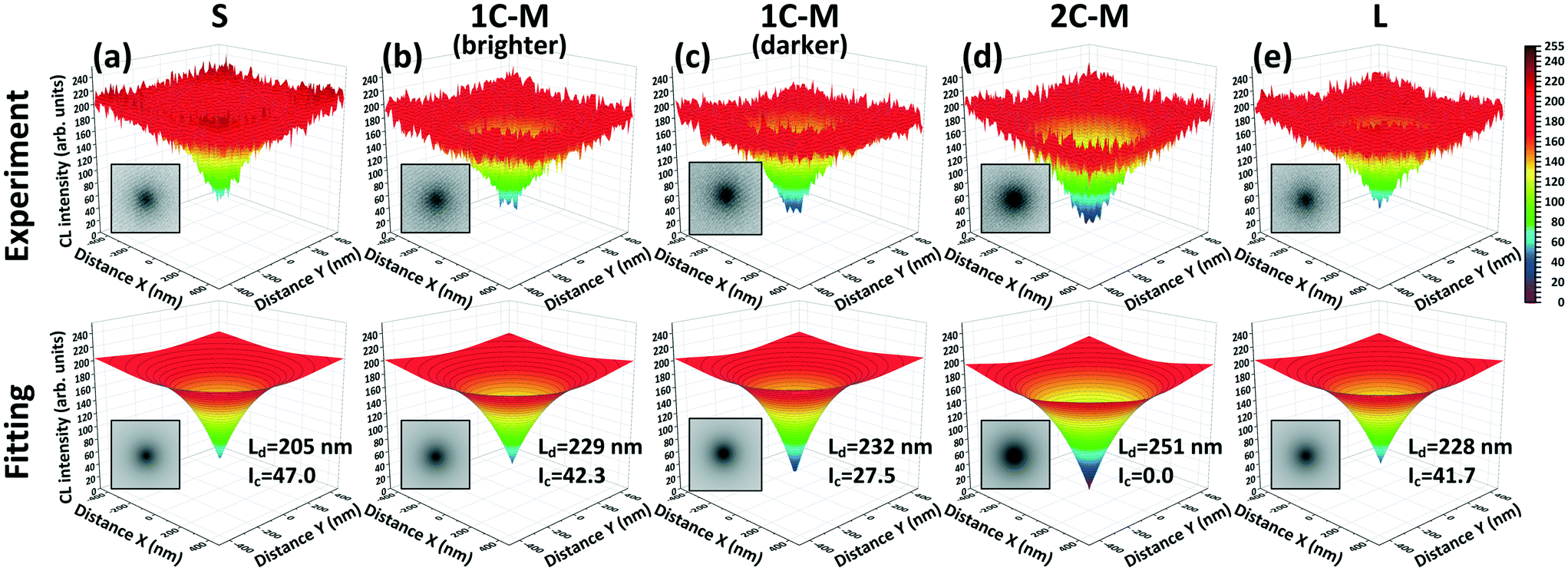
Fig. 5 shows the observation and fitting results for the representative dark spots corresponding to an S-pit, 1C-M-pits with 2 different contrast, a 2C-M-pit, and an L-pit. It is noted that we applied least-squares fitting in 2D rather than 1D because there is no need to designate the position of the dislocation core as long as the image used for fitting contains the entire area of the dark spot of interest. The core position is given by the fitting results. Therefore, 2D fitting greatly improves the accuracy compared with 1D fitting13,15,45 as the latter depends on where the cross-sectional profiles are drawn. From the fittings in Fig. 5, it is clear that the 2C-M-pit represents the strongest NRR center, which agrees with the direct observations from Fig. 3 and 4. The small Ic and large Ld indicate a higher recombination rate at the dislocation core and a wider range in which the carriers are attracted towards dislocations. A diffusion length of about 250 nm was reported by Rosner et al.,46 which is in close agreement with our findings, but these authors did not take into consideration the dislocation-type-dependence of diffusion length.
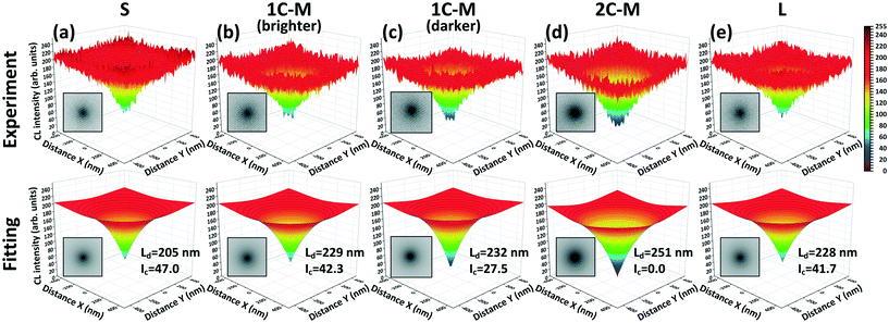 |
| | Fig. 5 Observation (upper row) and fitting (lower row) results for representative dark spots corresponding to (a) S-pit, (b) 1C-M-pit with a brighter contrast, (c) 1C-M-pit with a darker contrast, (d) 2C-M-pit, and (e) L-pit. Ld is the carrier diffusion length, and Ic is the CL intensity at the TD core. | |
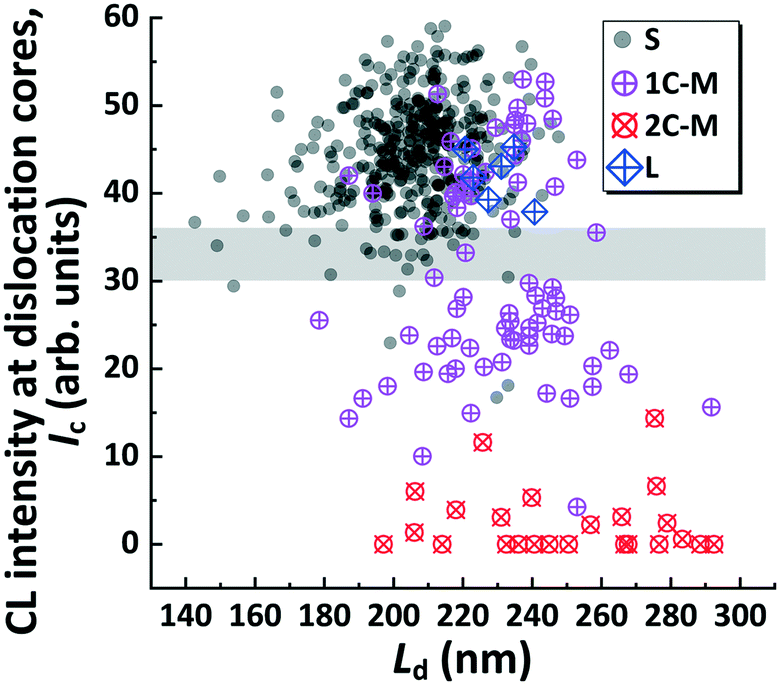
A distinct distribution is seen when increasing the number of fittings to 480 dislocations and correlating their Ic and Ld values with their pit sizes, as shown in Fig. 6. (The original CL images and the fitting results for more than 100 dark spots are given in the ESI† Fig. S2.) We found that the S-pits are concentrated in the upper-middle part of the graph with average values of Ic = 44.5 and Ld = 206.4 nm (Table 2). The L-pits, though very few, are also located in a limited area close to the swarm of S-pits, showing average values of Ic = 42.0 and Ld = 229.6 nm. The 2C-M-pits act as the strongest NRR centers among all dislocations and have average values of Ic = 2.5 and Ld = 248.8 nm. The most important observation from Fig. 6 is that there are two apparent sub-categories in the 1C-M-pits, which are roughly separated by a gap of Ic = 30–36 as indicated by the horizontal gray bar.
 |
| | Fig. 6
I
c and Ld of 480 dark spots obtained from the fitting and their correlation with pit sizes. | |
Table 2 A summary of Ic and Ld obtained by fitting 480 dark spots that correspond to dislocations with various pit sizes. Std. dev.: standard deviation
| Pit size |
Number |
Percentage |
I
c (Arb. units) |
L
d (nm) |
| Average |
Std. dev. |
Average |
Std. dev. |
| S |
374 |
78% |
44.5 |
6.3 |
206.4 |
16.9 |
| 1C-M (Ic > 36) |
31 |
6% |
43.9 |
4.8 |
227.9 |
15.6 |
| 1C-M (Ic < 30) |
45 |
9% |
22.3 |
5.5 |
231.8 |
22.0 |
| 2C-M |
24 |
5% |
2.5 |
3.8 |
248.8 |
28.0 |
| L |
6 |
1% |
42.0 |
2.7 |
229.6 |
6.8 |
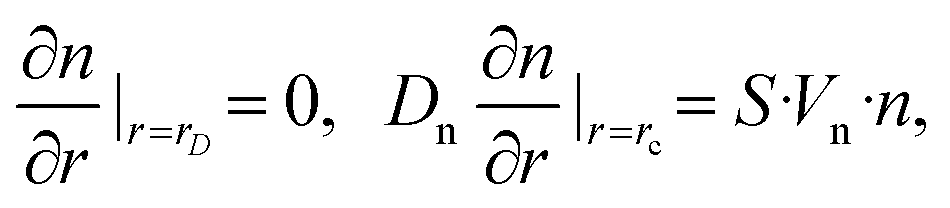
When considering the carrier diffusion around a dislocation, the solution to the steady-state diffusion equation for the two carrier types, n and p, should satisfy the following two sets of boundary conditions:44
| |  | (2) |
| |  | (3) |
where
rD is the radius of the cylinder considered for diffusion,
Dn and
Dp are the diffusion coefficients for electrons and holes, respectively,
S represents the fraction of electrically active sites at the dislocation cores, and
Vn and
Vp are the thermal velocities for electrons and holes, respectively.
44 From
eqn (2) and
(3), the only parameter that depends on the dislocation type is
S. It can be interpreted by considering that the different Burgers vectors lead to various dangling bond conditions and lattice distortions at the cores, which results in different
S values. A stronger NRR center is the result of a larger
S.
3.2 Etch pits and TEM – classification of dislocations via Burgers vectors
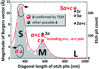
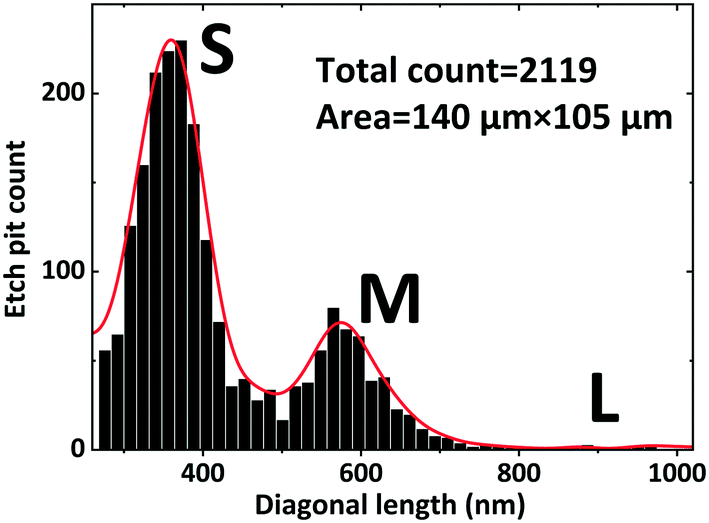
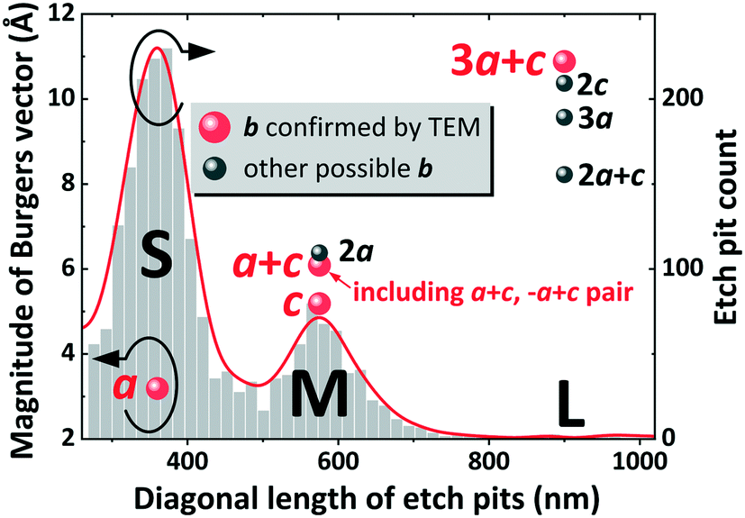
So far, we have correlated the NRR behavior with the pit size. We now turn to the structural properties of dislocations under each type of etch pit with a focus on the Burgers vector and line direction. Fig. 7 shows a histogram of the pit count as a function of size as measured by the diagonal length along the 〈110〉 direction (an example of automatically obtaining the pit sizes and coordinates from optical imagery is shown in the ESI† Fig. S3). The pit density is approximately 1.4 × 107 cm−2, which is close to the substrate average. The histogram indicates three size levels for the S-, M-, and L-pits, which is consistent with the early classifications from directly observing etch pit images (Fig. 3 and 4). The average size and percentage of the three pit types are summarized in Table 3. Compared with our previous study in which chemical etching was performed under similar conditions, we note the size ratio between the S-, M-, and L-pits as being very close to that obtained using several other commercial 2 inch HVPE substrates from different suppliers, though the exact percentage is different. This indicates that there is a structural property of dislocations that plays a dominant role in determining the pit size.
 |
| | Fig. 7 A histogram showing the pit count as a function of the pit size measured from the diagonal length along the 〈110〉 direction. | |
Table 3 Three size levels of etch pits and their percentages
| Pit size level |
Diagonal length |
Percentage |
| (nm) |
Normalized by S |
| S |
360 |
1.0 |
76% |
| M |
575 |
1.6 |
23% |
| L |
900 |
2.5 |
1% |
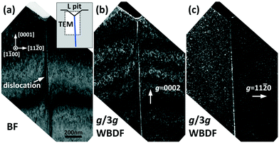
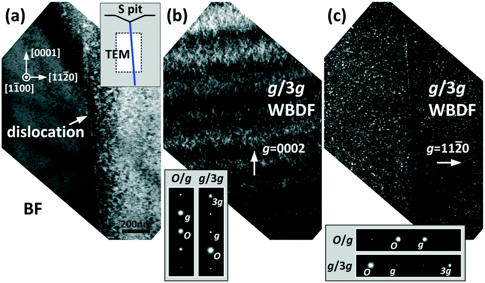
3.2.1 Dislocations under S-pits.
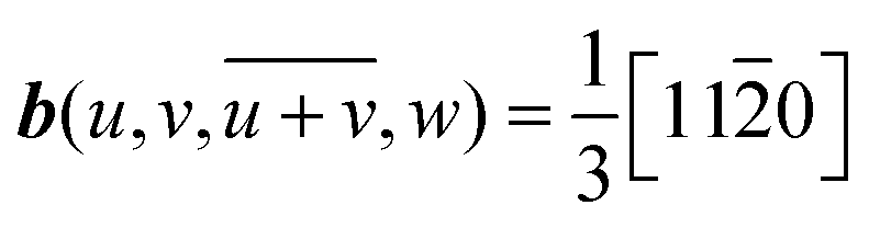
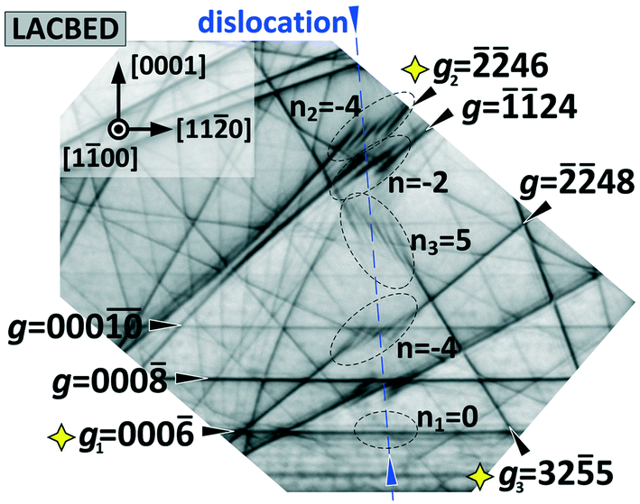
The TEM observations to determine the Burgers vectors began with a dislocation under an S-pit. Fig. 8(a)–(c) show the bright-field (BF) image and the g/3g WBDF images with g = 0002 and g = 110, respectively. The incident beam is along the [100] direction. The selected area diffraction patterns (SADPs) for each image are also shown, indicating the well-fulfilled g/3g conditions. The dislocation under investigation is out of contrast at g = 0002 but is on contrast at g = 110, indicating that it is a TED with an a-component Burgers vector. However, the magnitude and direction of b cannot be unambiguously determined at this point. Fig. 9 shows the LACBED pattern of the dislocation in which a convergent beam is used and the TEM foil is positioned out of the focal plane. Therefore, the dislocation line is not observed as clearly as that in the conventional mode. The dislocation position is indicated by a blue dashed line. When the dislocation intersects a Laue reflection line, the strain field around the dislocation causes the latter to split, causing nodes to appear. The number of nodes (n) satisfies the relationship g·b = n.39,47,48 Generating equations using at least 3 non-coplanar g values allows unambiguously solving the Burgers vector. In this case, the Burgers vector is determined to be 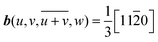 as deduced from,
| |  | (4) |
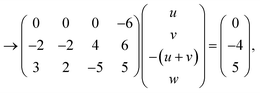
This is consistent with the g/3g WBDF observation. The WBDF and LACBED observations of several other dislocations under S-pits, both from this sample and from other HVPE substrates, confirm that the S-pits are always correlated with the 1a TEDs.
 |
| | Fig. 8 TEM images of the (a) bright-field (BF), (b) g/3g weak-beam dark-field (WBDF) with g = 0002, and (c) g/3g WBDF with g = 110. Selected area diffraction patterns (SADPs) for the WBDF are shown. The inset in (a) shows a schematic drawing showing the lift-out position with respect to the etch pit. | |
 |
| | Fig. 9 LACBED observation for the dislocation under the S-pit, which is the same dislocation as shown in Fig. 8. The blue dashed line is a guide to the dislocation position. The g values marked by yellow stars are used to create equations. | |
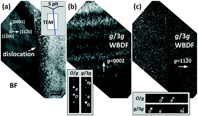
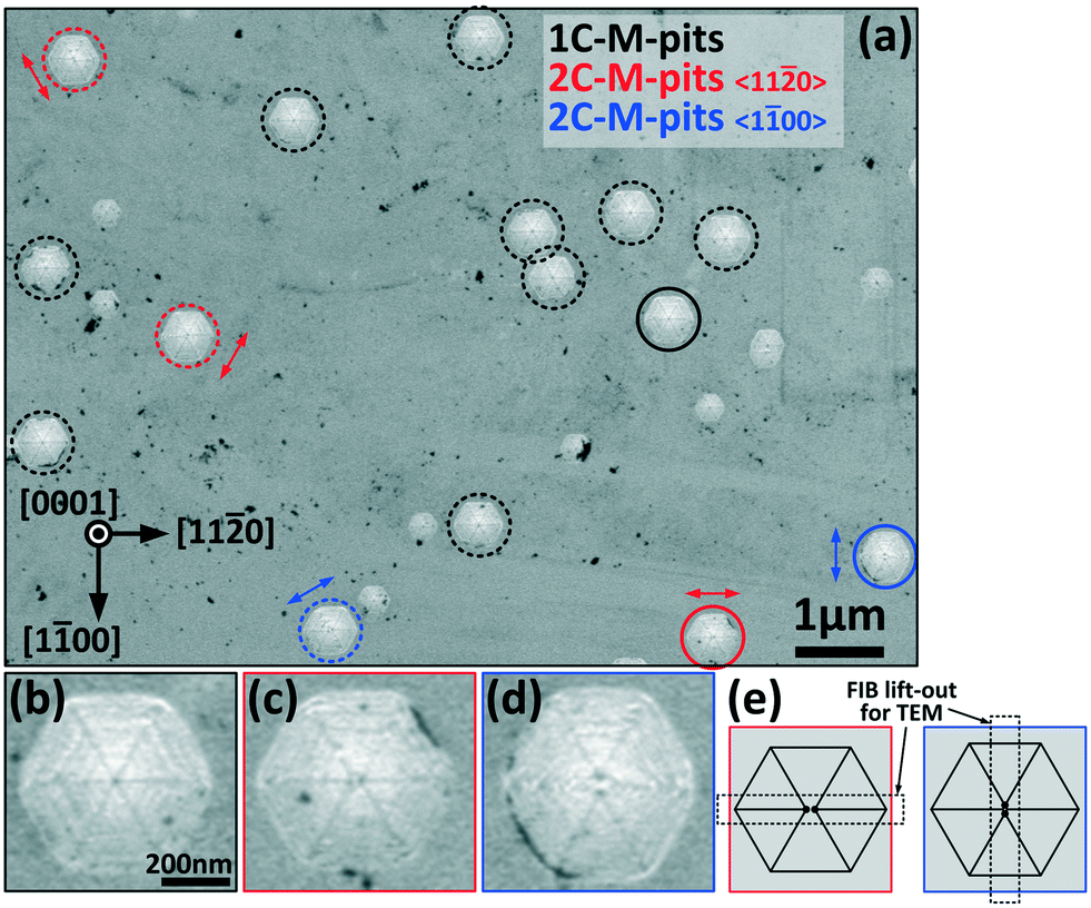
3.2.2 Dislocations under M-pits.
We now consider M-pits, which are the most complicated category among the three considered size levels. As discussed in section 3.1, M-pits can be grouped into two types based on their appearance: 1C-M-pit and 2C-M-pit. Furthermore, CL measurements (Fig. 6 and Table 2) indicate that (1) dislocations under 2C-M-pits are strong NRR centers, and (2) there are two sub-categories in 1C-M-pits that have weaker but different NRR rates. Fig. 10 shows an SEM image of an area containing several M-pits. The 1C-M-pits are marked by black circles and one example is enlarged in Fig. 10(b). For the 2C-M-pits, a close examination reveals that there are two different types, i.e., two different directions, in which the two cores separate from each other: the 〈110〉 direction or 〈100〉 direction [Fig. 10(c) and (d), respectively].
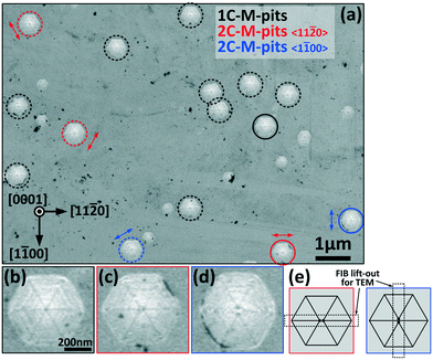 |
| | Fig. 10 (a) SEM image of an area containing several types of M-pits. Enlarged images of representative M-pits (marked with solid circles) with a (b) single-core, (c) double-core with a 〈110〉 separation, (d) double-core with a 〈100〉 separation, and (e) schematics of the 2C-M-pits and the directions of their FIB lift-out. The arrows indicate the direction of separation. The scale bar for (a) is 1 μm and that for (b), (c), and (d) is 200 nm. | |
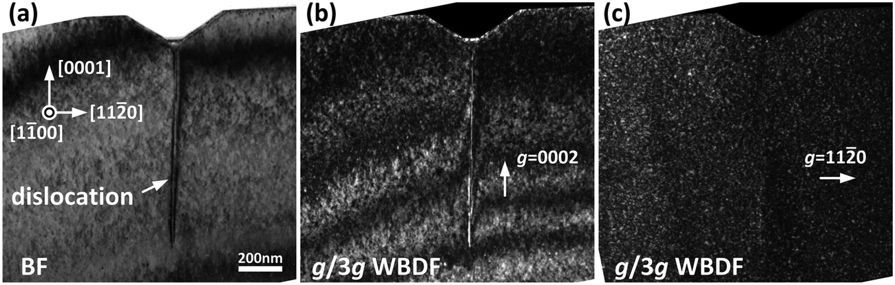
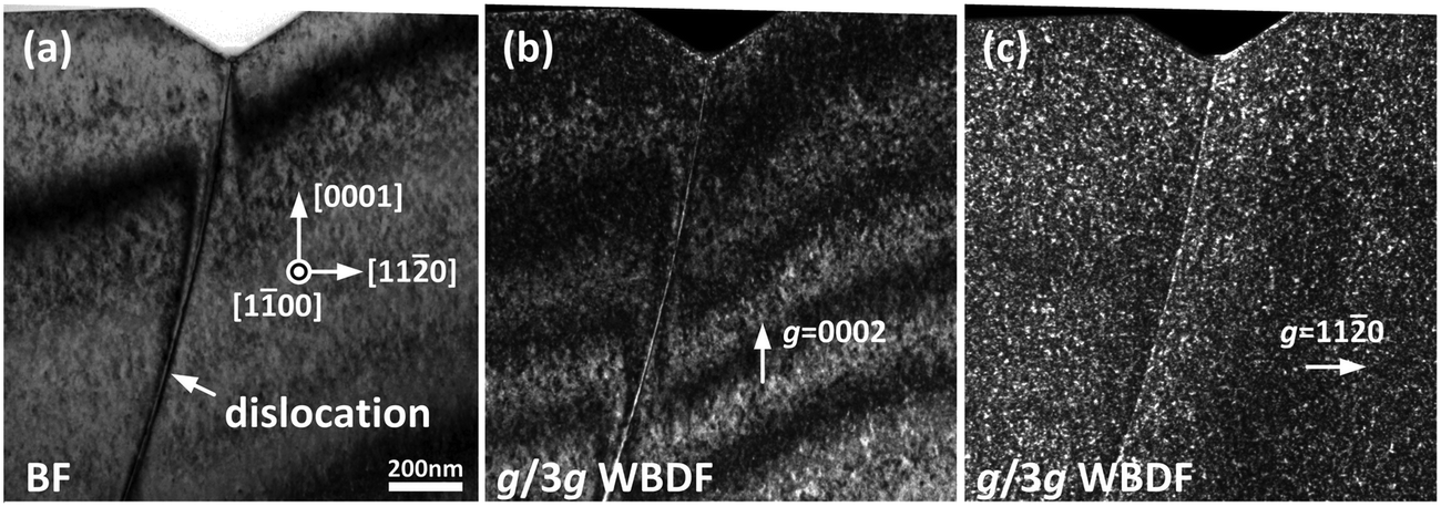
Firstly, we focus on 1C-M-pits. Fig. 11 and 12 show TEM images of dislocations under the 1C-M-pits with Ic = 43.7 (brighter 1C-M) and Ic = 20.7 (darker 1C-M), respectively. These dislocations are representatives as selected from the two sub-categories above and below the Ic = 30–36 gap (Fig. 6), respectively. Based on the g·b invisibility criterion, the g/3g WBDF images show that the brighter 1C-M-pit originates from a pure TSD without any a-component (Fig. 11), whereas the darker 1C-M-pit originates from a TMD having both a- and c-components (Fig. 12). The LACBED observations indicate that these are the 1c TSD and a + c TMD, respectively.
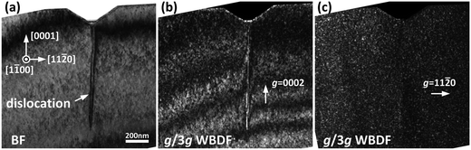 |
| | Fig. 11 TEM images of (a) BF, (b) g/3g WBDF with g = 0002, and (c) g/3g WBDF with g = 110 as observed from a typical “bright” 1C-M-pit with Ic = 43.7 and Ld = 225.1 nm. The results indicate that it is a 1c TSD. | |
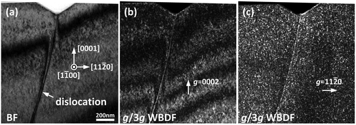 |
| | Fig. 12 TEM images of (a) BF, (b) g/3g WBDF with g=0002, and (c) g/3g WBDF with g = 110 as observed from a typical “dark” 1C-M-pit with Ic = 20.7 and Ld = 231.3 nm. The results indicate that it is an a + c TMD. | |
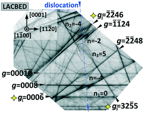
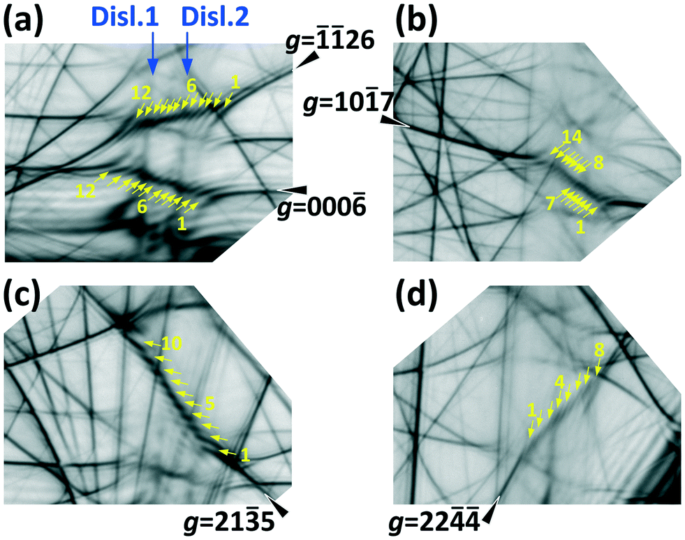
Secondly, 2C-M-pits are investigated. Fig. 13 shows TEM images of dislocations under a 2C-M-pit with a 〈110〉 separation. The WBDF images show two dislocation lines with a separation of approximately 42 nm. Their simultaneous visibility at g = 0002 and g = 110 indicates that they are both TMDs. The low magnification images [Fig. 13(d) and (e)] show that the two dislocations run perfectly along the c-axis and penetrate the entire 〈0001〉 thickness of the TEM foil. We further examined these dislocations using LACBED. Fig. 14 shows the LACBED patterns obtained for 5 non-coplanar g values. It is noted that as the two dislocations are spatially close (<100 nm), their strain fields overlap. The Burgers vector identified by LACBED, which relies on the strain-induced split of the Laue reflection lines, gives a combined b for the two dislocations.48 Creating equations using any 3 of the 5 g values shows that the combined b is [0002].
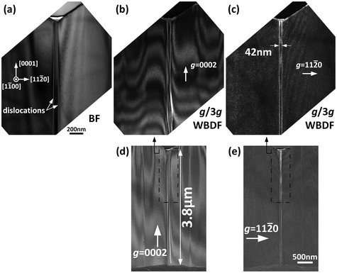 |
| | Fig. 13 TEM images of (a) BF, (b) g/3g WBDF with g = 0002, and (c) g/3g WBDF with g = 110 as observed from a pair of dislocations under a 2C-M-pit with the 〈110〉 separation. (d) and (e) show low-magnification images showing the entire 〈0001〉 thickness of the TEM foil. The results show that both dislocations are TMDs. The scale bar for (a)–(c) is 200 nm and that for (d) and (e) is 500 nm. | |
 |
| | Fig. 14 LACBED pattern as observed from the dislocations under a 2C-M-pit with the 〈110〉 separation, which are the same as shown in Fig. 13. Laue reflection lines using five different g vectors are shown in (a)–(d). | |
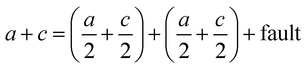
Comparing the LACBED results with those of g/3g WBDF leads to the important finding that the two dislocations under the 2C-M-pit are a (a + c) ~ (−a + c) TMD pair. They have opposite a-components, which cancel each other out, leaving a combined b of 2c without any a-component. The WBDF images show that the separation (∼42 nm) between two dislocations is well maintained over a long distance along the 〈0001〉 direction, indicating that the dislocation pair represents an energetically favorable and stable structure. Assuming that the strain energy of a dislocation is roughly proportional to the second power of its Burgers vector (E ∼ b2),49 we consider the following three scenarios for the TMD pair. (1) If the two TMDs with b1 = a + c and b2 = −a + c are far apart from each other, the total energy Etot follows Etot ∼ 2(a + c)2 = 2|a|2 + 2|c|2; (2) if the two TMDs completely react with each other to form a 2c TSD, Etot ∼ (2c)2 = 4|c|2; and (3) if the two TMDs are sufficiently close so that their in-plane strain fields cancel out but they each keep their independent c-components, Etot ∼ 2(c)2 = 2|c|2. Case (3) is energetically the most favorable, which was observed in the sample. The value of 42 nm is considered as a stable distance and corresponds to the lowest total strain energy.
It is noted that the above (a + c) ∼ (−a + c) TMD pair is composed of two perfect dislocations. This is distinct from the structure in which two identical ( ) partial dislocations that bound a prismatic fault are involved.25,26 We did not observe a contrast that would indicate that the region between the TMD pair is a fault. Moreover, the combined b of the pair is 2c rather than a + c.26 It is also noted that the above double-core structure is different from an open-core nanopipe as reported by some groups.20,33,50,51 The two dislocations show sharp and bright contrasts in the g/3g WBDF images, suggesting that they are dislocations rather than the sidewalls of a nanopipe. The LACBED results and the etch pit image also support this conclusion. TMD pairs with a similar distance (∼40 nm) of core separation were reported for InGaN,52 but the individual Burgers vector and line direction of these dislocations were not specified.
We now consider the other type of the 2C-M-pit. Fig. 15 shows TEM images of dislocations under a 2C-M-pit with a 〈100〉 separation. The dislocation pairs were not as perfectly contained in the TEM foil as was the previous case, presumably due to slight deviations of the dislocation line from the direction of FIB cutting. However, we still observed the short segments just beneath the etch pits and identified both dislocations as TMDs [Fig. 15(b) and (c)]. The separation distance is approximately 79 nm, which is much greater than the 〈110〉 separation case. We could not accurately determine the Burgers vectors for these dislocations using LACBED because they were too close to one of the foil surfaces and their strain field was not well preserved in the TEM foil. We estimate that the combined b has a c-component of −2c (the number of nodes is estimated to be 12) as shown in Fig. 15(d), but the a-component is uncertain based on the LACBED pattern. It is speculated that the 〈100〉 separation differs from the 〈110〉 separation due to a different relationship for the a-component of the two dislocations. That is, for the 〈110〉 separation, two dislocations have opposite a-components, but the two a-components for the 〈100〉 separation may form a 60° or 120° angle. Further investigation is needed to clarify the structures.
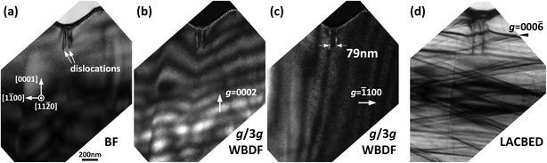 |
| | Fig. 15 TEM images of (a) BF, (b) g/3g WBDF with g = 0002, and (c) g/3g WBDF with g = 100 as observed from a pair of dislocations under a 2C-M-pit with the 〈100〉 separation. (d) The LACBED pattern obtained for g = 000![[6 with combining macron]](https://www.rsc.org/images/entities/char_0036_0304.gif) . The results show that both dislocations are TMDs. The scale bar for (a)–(c) is 200 nm. . The results show that both dislocations are TMDs. The scale bar for (a)–(c) is 200 nm. | |
3.2.3 Dislocations under L-pits.
Fig. 16 shows TEM images of dislocations under an L-pit, which is a TMD based on its visibility at two g values. LACBED (not shown) indicated that this is a 3a + c type TMD. This was confirmed in our previous studies35,36 that when KOH + Na2O2 is used as the etchant, the pit size is positively correlated with the magnitude of the Burgers vectors, which suggests that the strain field around a dislocation is the dominant factor that determines the pit size. This is considered as an important characteristic of the proposed etching method as produced with the Na2O2 additive.
 |
| | Fig. 16 TEM images of (a) BF, (b) g/3g WBDF with g = 0002, and (c) g/3g WBDF with g = 110 as observed from an L-pit. The results show that it is a TMD. | |
The distribution of pit size and its correlation with the Burgers vectors identified via TEM are summarized in Fig. 17. The dominant dislocation type is the 1a TED, which has the smallest Burgers vector and forms S-pits. The 1c TSDs and a + c TMDs (including the (a + c) ∼ (−a + c) TMD pairs) have larger Burgers vectors and are less common than the 1a TEDs, which form M-pits. The L-pits are attributed to dislocations with relatively large Burgers vectors. These are energetically unfavorable and may dissociate into multiple dislocations with smaller Burgers vectors. Therefore, these have much lower densities. While we did not capture some of the large Burgers vectors in this sample via TEM, including b = 2a, 2c, 3a, and 2a + c, our previous studies indicated that these Burgers vectors should lead to M- or L-pits, as shown in Fig. 17. Liliental-Weber53 reported that HVPE FS-GaN grown initially on sapphire had a comparable number of edge and screw dislocations, but the number of mixed dislocations was much higher. Lu et al.54 showed using the etch pit method and TEM analysis that half of the TDs in GaN thin films grown by metal–organic chemical vapor deposition (MOCVD) were TEDs and the other half were TSDs and TMDs with comparable densities. Albrecht et al.'s 400 μm-thick layers grown by HVPE on GaN substrates had percentages of 23%, 14%, and 63% for TEDs, TSDs, and TMDs, respectively.14 In the case of ammonothermal FS-GaN, Sintonen et al. reported percentages of 0%, 10%, and 90% for TEDs, TSDs, and TMDs, respectively, in a sample with a TD density of 3.5 × 104 cm−2,55 and 0%, 37%, and 63% in another sample with a TD density of 8.8 × 104 cm−2.6 Similar results for the ammonothermal FS-GaN were obtained in our previous study in which the Burgers vectors were determined using X-ray topography taken with seven g vectors.56 Compared to GaN thin films in early studies and FS-GaN grown by other methods, recent commercial HVPE substrates (TD density of ∼106 cm−2) from several suppliers typically show a dominant TED percentage of approximately 70–80%. The discrepancy in the percentage of each dislocation type in the literature suggests that dislocation structures depend strongly on the growth method, growth conditions, total dislocation density, layer thickness, and impurity species.
 |
| | Fig. 17 Distribution of pit size and its correlation with the Burgers vectors as identified by TEM. | |
Our results for the pit size and its correspondence with the Burgers vector conflict with the size ranking screw > mixed > edge in some publications where only KOH or a mixture of KOH and NaOH was used.14,16,19,57,58 The geometric features of etch pits in our study are also different from those formed with KOH54 or HCl gas.28 In these reports, the etch pits corresponding to TMDs have two-step facets, which appear as a combination of triangular and trapezoidal shapes when viewed along the cross-sectional direction.28
As the NRR behavior of each dislocation type is connected to the Burgers vector via the etch pit method and TEM observations, we summarize their correlations as follows. The strongest NRR center in our sample is the TMD pairs with a core separation of several tens of nanometers. These are composed of two TMDs with the same c-component but different a-components. The second strongest NRR center is the a + c TMD, whereas the other three types including the 1c TSD, 1a TED, and dislocations with a relatively large Burgers vector (revealed as L-pits) are similarly weak NRR centers. Among them, the TEDs are the weakest NRR centers (Table 2).
Meissner et al.16 studied an Fe-doped FS-GaN layer and Si-doped GaN films grown via HVPE using CL and the etch pit method. They confirmed a one-to-one correlation between the CL dark spots and the etch pits, but there was no direct relationship between the pit size and the contrast of the respective dark spot. The authors stated that any type of dislocation acts as an NRR center, but the different types of dislocations could not be attributed to the various dark spot contrasts.16 The first part of their conclusion is consistent with our results and those from ref. 11, but the second part is different from our findings. This discrepancy could be caused by differences in the impurity species and concentrations in their crystal from ours, which could make the Burgers vector less decisive. Hino et al.28 investigated Si-doped GaN epitaxial layers grown on a sapphire substrate via MOCVD. They used the decreased photoluminescence (PL) intensity as an indicator of NRR and used etch pits formed from HCl vapor-phase etching and TEM to determine the structural evaluation. The authors found that the PL intensity decreased with the total number of TSDs and TMDs but was insensitive to the TED density. Thus, they concluded that TSDs and TMDs were the dominant NRR centers in GaN epitaxial layers, whereas TEDs did not act as NRR centers. We note that the above conclusion was drawn based on the collective effect of dislocations on the radiative efficiency rather than observations of individual dislocations. Therefore, any direct connection between the Burgers vector and NRR behavior is complex. Albrecht et al.14 studied the contrast of CL dark spots and correlated them with dislocation types based on etch pits. The samples they used had similar growth methods, thicknesses, dislocation densities, and impurity concentrations to the sample from our study, but the authors found that the 1c TSDs are inactive as NRR centers in CL whereas TEDs and TMDs are active. Their results regarding TSDs disagree with our results and those in ref. 16 and 28. Yamamoto et al.12 used a TEM system with CL to simultaneously observe the NRR behavior and the Burgers vector of dislocations for a GaN/InGaN multi-quantum well structure. They found that the a + c TMDs were stronger NRR centers than the 1a TEDs, but the TSDs were not ranked because they were not present in the TEM foil. Their conclusion about TEDs and TMDs agrees with ours.
The NRR behavior and its correlation with the dislocation type have also been extensively studied for GaN in InGaN/GaN structures.59,60 For example, it was reported that all dislocation types are NRR centers in InGaN/GaN quantum wells (QWs), but TEDs directly act as NRR centers, whereas TSDs and TMDs indirectly affect the recombination through the geometrical factors of their surface pits.59,60 It is difficult to directly compare the NRR behavior for dislocations in FS-GaN with that in a device structure.
A model proposed by Hirsch et al.26 provides a possible explanation for why a + c TMDs are stronger NRR centers than the 1c TSDs in our observations (the two sub-categories belong to 1C-M-pits). The authors investigated the core structure of a + c TMDs using scanning TEM and confirmed the dissociation mechanism  . The total energy after dissociation was lower than that of the original a + c TMD. A stronger NRR is expected from the 2D fault bounded by partial dislocations compared with an undissociated 1c TSD, in addition to the fact that TMDs have a larger Burgers vector than TSDs. As the dissociation distance between partial dislocations is expected to be very small,26 we cannot judge whether the TMDs in our sample have any dissociation due to the limited resolution of the WBDF observations. Scanning TEM observations of TMDs viewed end-on will be conducted in future work.
3.3 Etch pits and MPPL – 3D visualization of dislocation lines
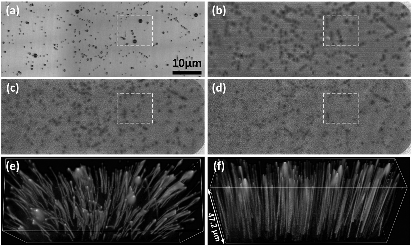
We now investigate the line direction of dislocations. Fig. 18(a) shows an etch pit image of an area selected for MPPL observations. All three pit size levels are seen in the image. A total of 201 MPPL images (Z-direction slices) were taken from Z = 0 (sample surface) to a deeper region at Z = 47.2 μm with a fixed ΔZ pitch. The refractive index of GaN (n = 2.36) was considered,61 and the selected Z value corresponds to actual depths in the substrate. Fig. 18(b)–(d) show the MPPL images at Z = 0, Z = 23.6, and Z = 47.2 μm, respectively. The dark spots observed at Z = 0 have positions that are consistent with the etch pits. The contrast of the dark spots is influenced by the presence of etch pits on the surface because the pit facets scatter incident light. Although this influence becomes negligible when Z > 5 μm, we do not discuss the spot contrast of MPPL and dislocation NRR behavior as we did for CL. Instead, we focus on the positions of dark spots and how they vary with depth. Comparing the dark spots marked with the white dashed frame in Fig. 18(b) with those in Fig. 18(c) and (d), both the number and position of the dark spots are different. Fig. 18(e) and (f) show a top-down view of the reconstructed 3D images of dislocations using the 201 MPPL images as viewed nearly along the c-axis and along the 〈10n〉 direction, respectively. The dislocation contrast is inverted for a better view.
 |
| | Fig. 18 (a) Etch pit image, and MPPL images taken from the same area at (b) Z = 0, (c) Z = 23.6 μm, and (d) Z = 47.2 μm. (e) and (f) show the 3D reconstructed dislocation images. The dislocation contrast is inverted for a better view. | |
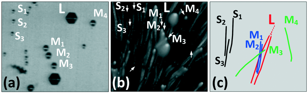
At the scale of several tens of micrometers, most of the dislocation lines are approximately parallel to the c-axis with some exceptions of notable tilting and curving. A closer examination (Fig. 19) reveals that the TEDs under S-pits (S1–S3) are nearly parallel to the c-axis with a tilting angle less than 5°. Dislocations under 2C-M-pits are perfectly along the c-axis, while dislocations with large tiltings are always related to the 1C-M-pits (M3, M4). Compared with the TEM observations described in section 3.2, we consider that the a + c TMDs might have large tiltings.26 For the L-pits, we found that there is a pair of dislocations that propagate under the etch pit (e.g., the one marked as “L”). Other examples of the dislocations under L-pits are shown in the 3D animation in the ESI.† In Fig. 19(a), it is clear that there is no etch pit near the L-pit besides M4; therefore, the two dislocations under the L-pits [Fig. 19(b)] are definitely associated with this L-pit. We speculate that L-pits, which correspond to dislocations with relatively large Burgers vectors, are the result of several dislocations with smaller Burgers vectors that merge. The TEM images in Fig. 16 show only a single dislocation line, suggesting that the merge point is deeper than the detection range of the TEM.
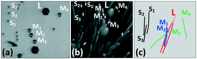 |
| | Fig. 19 (a) Etch pit image, (b) MPPL image, and (c) a schematic illustration of the dislocations marked by the white dashed frame in Fig. 18. | |
As the dislocation NRR behavior discussed here is based on the CL acquired from the top surface, dislocation tilting does not significantly affect our conclusions. We believe that the Burgers vector of a dislocation should play a more important role than the tilting in this study.10 However, it is noted that in real device structures, such as vertical GaN PN20 diodes or SBDs,21 the line direction of dislocations at deeper regions and the impurity accumulation around dislocations could significantly affect the optical and electrical properties. Finally, it is noted that not only foreign impurity species that accumulate around dislocations strongly affect the NRR behavior of dislocations, but the core structure of dislocations may also be important.26 Matsubara et al.62 showed using TEM that the dislocation cores may have several different atomic arrangements even though the Burgers vectors are the same. This means that even without the influence of impurities, the electronic states around the core could be different due to a locally varied stoichiometry.63 Further investigation is needed to classify these subjects.
Conclusions
We systematically investigated the NRR behavior of dislocations in an FS-GaN substrate grown via HVPE using CL. Its correlation with the structural properties of dislocations was evaluated using the etch pit method, TEM in the g/3g WBDF and LACBED modes, and MPPL. A statistical analysis based on one-to-one comparison of the CL dark spots with their corresponding etch pits was performed. The results show that all dislocation types act as NRR centers with an NRR rate at the dislocation cores that strongly depend on the pit size (S, 1C-M, 2C-M, and L). The etch pits were then used to connect the NRR behavior evaluated by CL to the Burgers vector of the dislocations as determined by TEM.
The findings are summarized in Table 4. It was found that dislocation pairs described as a 2C-M-pit are the strongest NRR centers among the considered dislocation types. These pairs are composed of an a + c and a −a + c TMD, or possibly other types of a + c TMDs. They run perfectly along the c-axis and have a stable distance of several tens of nanometers between the pair. These are followed by a + c TMDs (revealed as 1C-M-pits), TMDs with large Burgers vectors (revealed as L-pits), 1c TSDs (revealed as 1C-M-pits), and 1a TEDs (revealed as S-pits), in descending order of NRR rates. The 3D dislocation images visualized by MPPL reveal that most of the dislocations are nearly parallel to the c-axis, while the a + c TMDs are susceptible to large tilting. TMDs with a large Burgers vector may be the result of the reactions of several dislocations with smaller Burgers vectors.
Table 4 A summary of the results in this study
| Burgers vector (TEM) |
NRR (CL) |
Pit size (etching) |
Dislocation line (MPPL/TEM) |
Note |
| 1a |
Weak |
S |
Near <0001> |
Dominant type (∼76%) |
| 1c |
Weak |
1C-M |
Near <0001> |
|
|
a + c |
Intermedium |
1C-M |
Tilt from <0001> |
Possible dissociation |
|
a + c, −a + c pair |
Strong |
2C-M <110> |
Perfect <0001> |
Stable distance 42 nm |
|
a + c, a (60° or 120°) + c pair |
Strong |
2C-M <100> |
Perfect <0001> |
Inconclusive about a-component |
| 3a + c |
Weak |
L |
Near <0001> |
Possible dislocation reaction |
Authors' contributions
Y. Y. conceptualized the study, performed a part of the experiment, analysed the data and wrote the manuscript. Y. S. carried out the TEM observation. D. Y. prepared the TEM samples. K. S. carried out the chemical etching. Y. I. and M. S. performed the CL measurements. N. O. and K. T. prepared the FS-GaN. M. K., M. M. and T. E. provided discussion and advice on this study. Y. I. supervised this project. All authors have reviewed and approved the manuscript.
Data availability
Raw data were generated using the experimental equipment described in the main text. The data that supports the findings of this study are available within the article and the ESI.†
Conflicts of interest
There are no conflicts to declare.
Acknowledgements
This study was partially supported by “Knowledge Hub Aichi,” a Priority Research Project from the Aichi Prefectural Government III, Japan, JSPS KAKENHI, Japan, Grant No. 20K05176, and the New Energy and Industrial Technology Development Organization (NEDO), Japan.
Notes and references
- H. Amano, R. Collazo, C. de Santi, S. Einfeldt, M. Funato, J. Glaab, S. Hagedorn, A. Hirano, H. Hirayama, R. Ishii, Y. Kashima, Y. Kawakami, R. Kirste, M. Kneissl, R. W. Martin, F. Mehnke, M. Meneghini, A. Ougazzaden, P. J. Parbrook, S. Rajan, P. Reddy, F. Römer, J. Ruschel, B. Sarkar, F. Scholz, L. Schowalter, P. Shields, Z. Sitar, L. Sulmoni, T. Wang, T. Wernicke, M. Weyers, B. Witzigmann, Y.-R. Wu, T. Wunderer and Y. Zhang, J. Phys. D: Appl. Phys., 2020, 53, 503001, DOI:10.1088/1361-6463/aba64c.
- H. Amano, Y. Baines, E. Beam, M. Borga, T. Bouchet, P. R. Chalker, M. Charles, K. J. Chen, N. Chowdhury, R. Chu, C. De Santi, M. M. De Souza, S. Decoutere, L. Di Cioccio, B. Eckardt, T. Egawa, P. Fay, J. J. Freedsman, L. Guido, O. Häberlen, G. Haynes, T. Heckel, D. Hemakumara, P. Houston, J. Hu, M. Hua, Q. Huang, A. Huang, S. Jiang, H. Kawai, D. Kinzer, M. Kuball, A. Kumar, K. B. Lee, X. Li, D. Marcon, M. März, R. McCarthy, G. Meneghesso, M. Meneghini, E. Morvan, A. Nakajima, E. M. S. Narayanan, S. Oliver, T. Palacios, D. Piedra, M. Plissonnier, R. Reddy, M. Sun, I. Thayne, A. Torres, N. Trivellin, V. Unni, M. J. Uren, M. Van Hove, D. J. Wallis, J. Wang, J. Xie, S. Yagi, S. Yang, C. Youtsey, R. Yu, E. Zanoni, S. Zeltner and Y. Zhang, J. Phys. D: Appl. Phys., 2018, 51, 163001, DOI:10.1088/1361-6463/aaaf9d.
- K. Yamane, M. Ueno, H. Furuya, N. Okada and K. Tadatomo, J. Cryst. Growth, 2012, 358, 1, DOI:10.1016/j.jcrysgro.2012.07.038.
- H. Fujikura, T. Konno, T. Yoshida and F. Horikiri, Jpn. J. Appl. Phys., 2017, 56, 085503, DOI:10.7567/JJAP.56.085503.
- H. Fujikura, T. Konno, T. Suzuki, T. Kitamura, T. Fujimoto and T. Yoshida, Jpn. J. Appl. Phys., 2018, 57, 065502, DOI:10.7567/JJAP.57.065502.
- S. Sintonen, S. Suihkonen, H. Jussila, H. Lipsanen, T. O. Tuomi, E. Letts, S. Hoff and T. Hashimoto, J. Cryst. Growth, 2014, 406, 72, DOI:10.1016/j.jcrysgro.2014.08.022.
- D. Tomida, Q. Bao, M. Saito, R. Osanai, K. Shima, K. Kojima, T. Ishiguro and S. F. Chichibu, Appl. Phys. Express, 2020, 13, 055505, DOI:10.35848/1882-0786/ab8722.
- F. Kawamura, T. Iwahashi, K. Omae, M. Morishita, M. Yoshimura, Y. Mori and T. Sasaki, Jpn. J. Appl. Phys., 2003, 42, L4, DOI:10.1143/JJAP.42.L4.
- H. M. Ng, D. Doppalapudi, T. D. Moustakas, N. G. Weimann and L. F. Eastman, Appl. Phys. Lett., 1998, 73, 821, DOI:10.1063/1.122012.
- N. G. Weimann, L. F. Eastman, D. Doppalapudi, H. M. Ng and T. D. Moustakas, J. Appl. Phys., 1998, 83, 3656, DOI:10.1063/1.366585.
- T. Sugahara, H. Sato, M. Hao, Y. Naoi, S. Kurai, S. Tottori, K. Yamashita, K. Nishino, L. Romano and S. Sakai, Jpn. J. Appl. Phys., 1998, 37, L398, DOI:10.1143/JJAP.37.L398.
- N. Yamamoto, H. Itoh, V. Grillo, S. F. Chichibu, S. Keller, J. S. Speck, S. P. DenBaars, U. K. Mishra, S. Nakamura and G. Salviati, J. Appl. Phys., 2003, 94, 4315, DOI:10.1063/1.1598632.
- N. Pauc, M. R. Phillips, V. Aimez and D. Drouin, Appl. Phys. Lett., 2006, 89, 161905, DOI:10.1063/1.2357881.
- M. Albrecht, J. L. Weyher, B. Lucznik, I. Grzegory and S. Porowski, Appl. Phys. Lett., 2008, 92, 231909, DOI:10.1063/1.2928226.
- N. Ino and N. Yamamoto, Appl. Phys. Lett., 2008, 93, 232103, DOI:10.1063/1.3040310.
- E. Meissner, S. Schweigard, J. Friedrich, T. Paskova, K. Udwary, G. Leibiger and F. Habel, J. Cryst. Growth, 2012, 340, 78, DOI:10.1016/j.jcrysgro.2011.12.043.
- B. S. Simpkins, E. T. Yu, P. Waltereit and J. S. Speck, J. Appl. Phys., 2003, 94, 1448, DOI:10.1063/1.1586952.
- T. Kachi and T. Uesugi, Sens. Mater., 2013, 25, 219, DOI:10.18494/SAM.2013.881.
- S. Usami, Y. Ando, A. Tanaka, K. Nagamatsu, M. Deki, M. Kushimoto, S. Nitta, Y. Honda, H. Amano, Y. Sugawara, Y. Yao and Y. Ishikawa, Appl. Phys. Lett., 2018, 112, 182106, DOI:10.1063/1.5024704.
- S. Usami, A. Tanaka, H. Fukushima, Y. Ando, M. Deki, S. Nitta, Y. Honda and H. Amano, Jpn. J. Appl. Phys., 2019, 58, SCCB24, DOI:10.7567/1347-4065/ab1250.
- T. Hamachi, T. Tohei, M. Imanishi, Y. Mori and A. Sakai, Jpn. J. Appl. Phys., 2019, 58, SCCB23, DOI:10.7567/1347-4065/ab1392.
- T. Nakano, Y. Harashima, K. Chokawa, K. Shiraishi, A. Oshiyama, Y. Kangawa, S. Usami, N. Mayama, K. Toda, A. Tanaka, Y. Honda and H. Amano, Appl. Phys. Lett., 2020, 117, 012105, DOI:10.1063/5.0010664.
- J.-L. Farvacque, Mater. Sci. Eng., B, 1996, 42, 110, DOI:10.1016/s0921-5107(96)01691-1.
- Z. Z. Bandić, P. M. Bridger, E. C. Piquette and T. C. McGill, Solid-State Electron., 2000, 44, 221, DOI:10.1016/S0038-1101(99)00227-0.
- P. D. Nellist, P. B. Hirsch, S. Rhode, M. K. Horton, J. G. Lozano, A. Yasuhara, E. Okunishi, S. Zhang, S. L. Sahonta, M. J. Kappers, C. J. Humphreys and M. A. Moram, J. Phys.: Conf. Ser., 2014, 522, 012037, DOI:10.1088/1742-6596/522/1/012037.
- P. B. Hirsch, J. G. Lozano, S. Rhode, M. K. Horton, M. A. Moram, S. Zhang, M. J. Kappers, C. J. Humphreys, A. Yasuhara, E. Okunishi and P. D. Nellist, Philos. Mag., 2013, 93, 3925, DOI:10.1080/14786435.2013.797617.
- J. Elsner, R. Jones, P. K. Sitch, V. D. Porezag, M. Elstner, T. Frauenheim, M. I. Heggie, S. Öberg and P. R. Briddon, Phys. Rev. Lett., 1997, 79, 3672, DOI:10.1103/PhysRevLett.79.3672.
- T. Hino, S. Tomiya, T. Miyajima, K. Yanashima, S. Hashimoto and M. Ikeda, Appl. Phys. Lett., 2000, 76, 3421, DOI:10.1063/1.126666.
- Y. Xin, S. J. Pennycook, N. D. Browning, P. D. Nellist, S. Sivananthan, F. Omnès, B. Beaumont, J. P. Faurie and P. Gibart, Appl. Phys. Lett., 1998, 72, 2680, DOI:10.1063/1.121097.
- L. Sang, B. Ren, M. Sumiya, M. Liao, Y. Koide, A. Tanaka, Y. Cho, Y. Harada, T. Nabatame, T. Sekiguchi, S. Usami, Y. Honda and H. Amano, Appl. Phys. Lett., 2017, 111, 122102, DOI:10.1063/1.4994627.
- T. Hamachi, S. Takeuchi, T. Tohei, M. Imanishi, M. Imade, Y. Mori and A. Sakai, J. Appl. Phys., 2018, 123, 161417, DOI:10.1063/1.5011345.
- Y. Lei, H. Lu, D. Cao, D. Chen, R. Zhang and Y. Zheng, Solid-State Electron., 2013, 82, 63, DOI:10.1016/j.sse.2013.01.007.
- M. Moseley, A. Allerman, M. Crawford, J. J. Wierer, M. Smith and L. Biedermann, J. Appl. Phys., 2014, 116, 053104, DOI:10.1063/1.4891830.
- K. Kanaya and S. Okayama, J. Phys. D: Appl. Phys., 1972, 5, 43, DOI:10.1088/0022-3727/5/1/308.
- Y. Yao, Y. Ishikawa, Y. Sugawara, H. Saitoh, K. Danno, H. Suzuki, Y. Kawai and N. Shibata, Jpn. J. Appl. Phys., 2011, 50, 075502, DOI:10.1143/JJAP.50.075502.
- Y. Yao, Y. Ishikawa, Y. Sugawara, D. Yokoe, M. Sudo, N. Okada and K. Tadatomo, Superlattices Microstruct., 2016, 99, 83, DOI:10.1016/j.spmi.2016.05.002.
-
D. B. Williams and C. B. Carter, Transmission Electron Microscopy: A Textbook for Materials Science, Springer Science+Business Media, 2009, pp. 463–481 Search PubMed.
-
D. Hull and D. J. Bacon, Introduction to dislocations, Elsevier Ltd., Oxford, 5th edn, 2011, pp. 24–27 Search PubMed.
- D. Cherns, C. J. Kiely and A. R. Preston, Ultramicroscopy, 1988, 24, 355 CrossRef CAS.
-
D. B. Williams and C. B. Carter, Transmission Electron Microscopy: A Textbook for Materials Science, Springer Science+Business Media, 2009, pp. 323–345 Search PubMed.
- Y. Sugawara, M. Nakamori, Y. Yao, Y. Ishikawa, K. Danno, H. Suzuki, T. Bessho, S. Yamaguchi, K. Nishikawa and Y. Ikuhara, Appl. Phys. Express, 2012, 5, 081301, DOI:10.1143/APEX.5.081301.
- Y. Sugawara, Y. Ishikawa, A. Watanabe, M. Miyoshi and T. Egawa, AIP Adv., 2016, 6, 045020, DOI:10.1063/1.4948451.
- K. Kumakura, T. Makimoto, N. Kobayashi, T. Hashizume, T. Fukui and H. Hasegawa, Appl. Phys. Lett., 2005, 86, 052105, DOI:10.1063/1.1861116.
- S. Y. Karpov and Y. N. Makarov, Appl. Phys. Lett., 2002, 81, 4721, DOI:10.1063/1.1527225.
- W. Liu, J. F. Carlin, N. Grandjean, B. Deveaud and G. Jacopin, Appl. Phys. Lett., 2016, 109, 042101, DOI:10.1063/1.4959832.
- S. Rosner, E. Carr, M. Ludowise, G. Girolami and H. Erikson, Appl. Phys. Lett., 1997, 70, 420, DOI:10.1063/1.118322.
- D. Cherns and J. P. Morniroli, Ultramicroscopy, 1994, 53, 167, DOI:10.1016/0304-3991(94)90007-8.
- F. A. Ponce, D. Cherns, W. T. Young and J. W. Steeds, Appl. Phys. Lett., 1996, 69, 770, DOI:10.1063/1.117886.
-
J. P. Hirth and J. Lothe, Theory of dislocations, Krieger Publishing Co., Florida, 2nd edn, 1992, pp. 59–95 Search PubMed.
- A. Y. Polyakov, E. B. Yakimov, N. B. Smirnov, A. V. Govorkov, A. S. Usikov, H. Helava, Y. N. Makarov and I. Lee, J. Vac. Sci. Technol., B, 2014, 32, 051212, DOI:10.1116/1.4895658.
- J. W. P. Hsu, M. J. Manfra, R. J. Molnar, B. Heying and J. S. Speck, Appl. Phys. Lett., 2002, 81, 79, DOI:10.1063/1.1490147.
- F. C.-P. Massabuau, P. Chen, M. K. Horton, S. L. Rhode, C. X. Ren, T. J. O'Hanlon, A. Kovács, M. J. Kappers, C. J. Humphreys, R. E. Dunin-Borkowski and R. A. Oliver, J. Appl. Phys., 2017, 121, 013104, DOI:10.1063/1.4973278.
- Z. Liliental-Weber, Jpn. J. Appl. Phys., 2014, 53, 100205, DOI:10.7567/JJAP.53.100205.
- L. Lu, Z. Y. Gao, B. Shen, F. J. Xu, S. Huang, Z. L. Miao, Y. Hao, Z. J. Yang, G. Y. Zhang, X. P. Zhang, J. Xu and D. P. Yu, J. Appl. Phys., 2008, 104, 123525, DOI:10.1063/1.3042230.
- S. Sintonen, S. Suihkonen, H. Jussila, A. Danilewsky, R. Stankiewicz, T. O. Tuomi and H. Lipsanen, Appl. Phys. Express, 2014, 7, 091003, DOI:10.7567/APEX.7.091003.
- Y. Yao, Y. Ishikawa, Y. Sugawara, Y. Takahashi and K. Hirano, J. Electron. Mater., 2018, 47, 5007, DOI:10.1007/s11664-018-6252-3.
- J. L. Weyher, S. Lazar, L. Macht, Z. Liliental-Weber, R. J. Molnar, S. Müller, V. G. M. Sivel, G. Nowak and I. Grzegory, J. Cryst. Growth, 2007, 305, 384, DOI:10.1016/j.jcrysgro.2007.03.030.
- J. L. Weyher, Superlattices Microstruct., 2006, 40, 279, DOI:10.1016/j.spmi.2006.06.011.
- D. Cherns, S. J. Henley and F. A. Ponce, Appl. Phys. Lett., 2001, 78, 2691, DOI:10.1063/1.1369610.
- J. Abell and T. D. Moustakas, Appl. Phys. Lett., 2008, 92, 091901, DOI:10.1063/1.2889444.
- T. Tanikawa, K. Ohnishi, M. Kanoh, T. Mukai and T. Matsuoka, Appl. Phys. Express, 2018, 11, 031004, DOI:10.7567/APEX.11.031004.
- T. Matsubara, K. Sugimoto, S. Goubara, R. Inomoto, N. Okada and K. Tadatomo, J. Appl. Phys., 2017, 121, 185101, DOI:10.1063/1.4983254.
- J. E. Northrup, Appl. Phys. Lett., 2001, 78, 2288, DOI:10.1063/1.1361274.
Footnote |
| † Electronic supplementary information (ESI) available: See the ESI for information about TEM observation of a dent, fitting of CL dark spots, etch pit analysis, and an animation of 3D visualization of dislocations. See DOI: 10.1039/d0ce01344g |
|
| This journal is © The Royal Society of Chemistry 2020 |
Click here to see how this site uses Cookies. View our privacy policy here. 
 Open Access Article
 This Open Access Article is licensed under a
  *a,
Yoshihiro
Sugawara
*a,
Yoshihiro
Sugawara


 as deduced from,
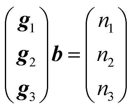


 ) partial dislocations that bound a prismatic fault are involved.25,26 We did not observe a contrast that would indicate that the region between the TMD pair is a fault. Moreover, the combined b of the pair is 2c rather than a + c.26 It is also noted that the above double-core structure is different from an open-core nanopipe as reported by some groups.20,33,50,51 The two dislocations show sharp and bright contrasts in the g/3g WBDF images, suggesting that they are dislocations rather than the sidewalls of a nanopipe. The LACBED results and the etch pit image also support this conclusion. TMD pairs with a similar distance (∼40 nm) of core separation were reported for InGaN,52 but the individual Burgers vector and line direction of these dislocations were not specified.
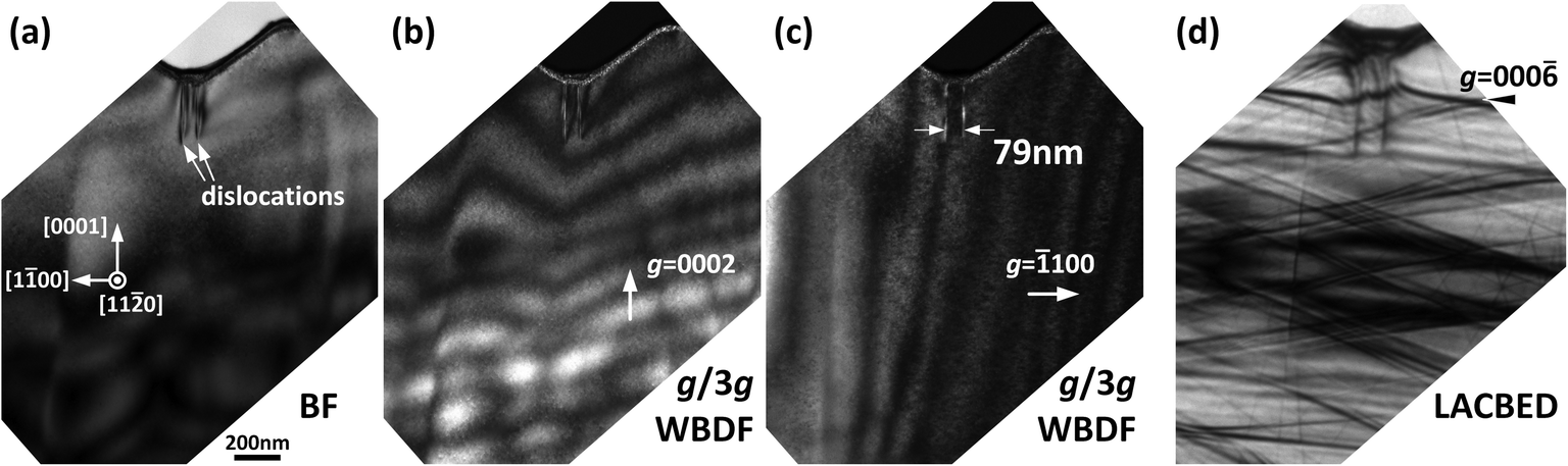
 . The total energy after dissociation was lower than that of the original a + c TMD. A stronger NRR is expected from the 2D fault bounded by partial dislocations compared with an undissociated 1c TSD, in addition to the fact that TMDs have a larger Burgers vector than TSDs. As the dissociation distance between partial dislocations is expected to be very small,26 we cannot judge whether the TMDs in our sample have any dissociation due to the limited resolution of the WBDF observations. Scanning TEM observations of TMDs viewed end-on will be conducted in future work.