DOI:
10.1039/D0CE01236J
(Paper)
CrystEngComm, 2020,
22, 8236-8242
Single crystal growth of GdB6 by the optical floating-zone technique
Received
24th August 2020
, Accepted 22nd October 2020
First published on 23rd October 2020
Abstract
A high-quality and large-sized GdB6 single crystal was successfully prepared by using the optical floating zone method to accurately control the temperature and composition of the molten zone. A GdB6 [100] single crystal 25 mm in length and 5 mm in diameter was obtained. The full width at half-maximum (FWHM) of the X-ray rocking curves was 0.227°, which indicated that the as-grown GdB6 single crystal had a high quality. The maximum thermionic emission current density of the GdB6 single crystal was 6.73 A cm−2 at U = 4000 V and T = 1873 K, and the average work function was 2.99 eV. Combining first-principles calculations and experiments, the work function was found to monotonically increase as the size of the GdB6 single crystal changed from nanostructure (1D) to bulk (3D).
Introduction
Gadolinium hexaboride (GdB6) single crystal has attracted considerable research interest due to its unique and plentiful physical properties such as magnetic transport, electronic emission, high optical absorption or transmittance coefficient and so on.1–10 GdB6, with a half-filled 4f electron structure and known as a member of the rare-earth hexaboride family, has a simple cubic CaB6-type structure with octahedra of B in the cube corners and Gd in the cube center,1 which is believed to be responsible for two magnetic transitions at low temperatures,2–5 high neutron absorption,6 strong light absorption in the near infrared region7 and low work function.8 In particular, the high brightness and metal-like conductivity (∼10−5 Ω cm) make the GdB6 single crystal a promising cathode material.9,10 Studies showed that the cold field electron emission capability of a GdB6 single nanowire was more than 5 times larger than that of a LaB6 nanowire under the same conditions.11–13
However, from the aspect of thermionic electron emission, GdB6 single crystals with a large size (>5 mm in the diameter) have been investigated insufficiently and controversially up to now. The work function of GdB6 single crystals with a large size is reported to widely range from 3.1 eV to 3.8 eV (ref. 14–17) while the work function of single-crystalline GdB6 nanowires is only 1.5 eV,11 which is considered to have the lowest work function among the rare earth hexaboride family. Therefore, further investigations of its thermionic emission properties including the work function are needed. It is well known that the thermionic emission properties of cathodes are sensitive to the quality of single crystals and the preparation method. Although the preparation of GdB6 single crystals has been reported since the 1980s, the GdB6 single crystals are always grown accompanied with GdB4 impurities. According to the phase diagram shown in Fig. 1, GdB6 melts incongruently by a peritectic reaction. Moreover, the composition range and melting temperatures of GdB4 and GdB6 are close to each other. Additionally, the volatility of Gd and B at high temperature may change the composition of the molten zone.14,18 All of the above show that GdB6 is a metastable phase and easily decomposes into GdB4 impurity during crystal growth, and this impurity can seriously weaken the quality of the as-grown single crystal. Even if a GdB6 single crystal is cut from the as-grown crystal, the impurities have already damaged the quality of the crystal.15 Another way to avoid the formation of GdB4 impurities is the addition of excess boron into a polycrystalline rod, which can effectively avoid GdB4 impurities, but excess boron can also weaken the thermionic emission properties of the GdB6 single crystal, with the work function of which being as high as 4.2 eV.17 Therefore, the preparation of high-purity GdB6 single crystals without GdB4 impurity becomes worthy and necessary.
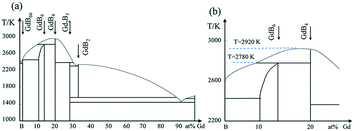 |
| | Fig. 1 (a) Phase diagram of the B–Gd binary system. (b) Schematic diagram in detail. | |
The floating zone melting technique is a widely employed method to prepare large-sized single crystals with a high melting point and extreme melt reactivity.19–22 Compared to conventional crystal growth methods such as the Bridgman and Czochralski methods, the primary advantages of this crucible-free method are it has no contamination or expansion/contraction problems.23 The vertical inductive zone melting technique has been the main method used to prepare large-sized GdB6 single crystals for decades.24 Although this method has high efficiency for purifying the impurities such as oxygen, iron, carbon and so on, impurities caused by melting incongruently are difficult to avoid during crystal growth and are always formed on the periphery of crystals due to the instability of the floating zone.25,26 Unlike the vertical inductive zone melting technique, optical floating zone with radiation heating has high stability of the melting zone. By employing an additional technique, the optical floating zone method can make impurities completely disappear for the growth of metastable single crystals.27–29 However, the details of preparing GdB6 single crystals without GdB4 impurities by the optical floating zone method have not been given so far.
Therefore, we present the successful growth of high-quality GdB6 single crystals without impurities by the optical floating-zone technique by strictly controlling the length of the molten zone and the lamp power in this work. The characteristics and thermionic emission properties of the as-grown single crystal were studied. The maximum emission current density of GdB6 is 6.73 A cm−2 measured at 1873 K under an applied voltage of 4000 V. The average work function is 2.99 eV. Combining with first-principles calculations, the wide difference in the work function of large-sized GdB6 single crystals and nanowires can be revealed, which is helpful to understand the difference in the work function of rare earth hexaborides with different sizes.
Experimental
Materials and methods
Commercial GdH2 (purity 99.9%, mean particle size 35 μm, Hunan Rare Metal Material Research Institute, Changsha, China) and B powders (purity 99.5%, mean particle size 20 μm, Jiangxi Ketai Advanced Materials Co., Ltd. Gaoan, China) were firstly mixed in a stainless steel jar, which was placed in a glovebox with an Ar atmosphere and O content lower than 10 ppm. The homogenization of the powder mixtures was carried out in a planetary high energy ball mill (QM-QX2) under the process parameters of rotation rate R = 350 r min−1 and time t = 3 h. The powder mixtures were then put into a hollow graphite die with an inner diameter of 20.4 mm in the glovebox. After prepressing, the die was covered with porous graphite felt to maintain thermal insulation and then placed into a spark plasma sintering furnace (SPS) (LABOX-350, Sinter Land Inc., Japan). Bulk polycrystalline GdB6 was synthesized at a sintering temperature T = 973–1773 K, heating rate R = 30–100 K min−1, axial pressure P = 1–12.6 kN and dwell time t = 5 min. After that, the furnace was then cooled to room temperature. During sintering, the temperature was monitored using an infrared thermometer.
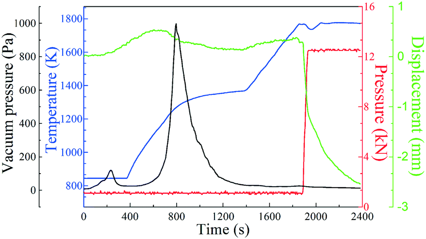
A GdB6 single crystal was grown by the optical floating zone melting method under an Ar atmosphere, and the furnace (FZ-T-20000-X-I-VPO-PC, Crystal Systems Inc, Japan) was equipped with 4 × 5 kW xenon lamps focused by four polished elliptical mirrors, as shown in Fig. 2. A polycrystalline GdB6 rod 6 mm in diameter and 40 mm in length was in the upper rotary shaft, and a [100] LaB6 single crystal with the same diameter was used as the seed crystal located on the lower rotary shaft. Thereafter, a quartz tube with a 40 mm internal diameter was loaded.
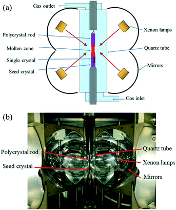 |
| | Fig. 2 (a) Schematic diagram and (b) photograph of the optical floating zone growth furnace. | |
The quality and structure of the GdB6 single crystals were characterized by inductively coupled plasma mass spectrometry (ICP-MS, X Series 2, Thermo Fisher, USA), high-resolution X-ray diffraction (XRD, X Pert Pro MPD, PANalytical B V, Holland) and X-ray Laue diffraction (JF-3, Liaodong, China). The microstructures and the component of the crystal were characterized using scanning electron microscopy (SEM, Sigma, Zeiss, Germany) with energy dispersive spectroscopy (EDS, X-MaxN, Oxford, England). Cu-Kα radiation was used in high-resolution X-ray diffraction and X-ray Laue diffraction.
Single crystal GdB6 samples were cut into 1 × 1 × 3 mm. After treatment with standard metallographic techniques, the specimen was cleaned with saturated NaOH solution and dilute nitric acid solution for 30 min, respectively. After drying, thermionic emission current tests were performed in a vacuum chamber with a pressure of 5 × 10⁻⁵ Pa. The GdB6 was heated at 1873 K for 3 h to clean the surface before measuring the current density. The variation of thermionic emission current with the applied voltage is recorded at a temperature ranging from 1673 K to 1873 K, which was monitored using a disappearing filament optical pyrometer (WGG2-201N, SAIL, Shanghai) within ±2% accuracy. The distance between the anode and cathode is 0.8 mm.
Computational methods
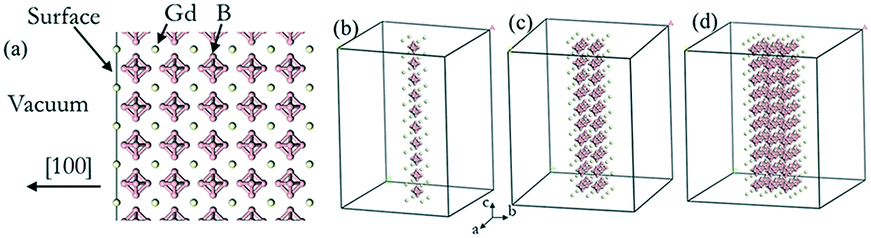
The calculations of the work function of GdB6 were performed based on density functional theory (DFT) implemented in the VASP code. Ultra-soft pseudopotentials were employed together with the generalized gradient approximation (GGA) in the Perdew–Burke–Ernzerhof (PBE) exchange–correlation and a 400 eV energy cut off was used in our calculations.30 An effective on-site Coulomb repulsion Ueff = 8.0 eV with the method of self-interaction correction (SIC) for the Gd-4f orbitals was applied. As shown in Fig. 3(a), 5 layer supercells with a 20 Å vacuum corresponding to the [100] lattice vectors were applied for the calculations of bulk GdB6. For the calculations of GdB6 nanowires, the structures were n × n × ∞ (n = 1, 2, and 3) quasi 1-D nanowires with a more than 24 Å vacuum along the a and b axes, as shown in Fig. 3(b–d). 1 × 16 × 16 and 1 × 1 × 16 k-points were adopted for the bulk and nanowire calculations, respectively. Geometry optimization was employed since the structural distortion on the surface was not ignorable.
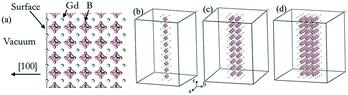 |
| | Fig. 3 (a) Gd terminations of the (100) surface of GdB6. (b)–(d) The structures of n × n × ∞ (n = 1, 2, and 3) quasi 1-D nanowires of GdB6. | |
Results and discussion
Polycrystalline sample preparation and single crystal growth
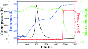
Fig. 4 shows the preparation process of polycrystalline GdB6 using SPS. The preparation of polycrystalline GdB6 can be divided into two stages: dehydrogenation and liquid-phase synthesis. In the first stage, GdH2 is decomposed into Gd metal and H2 at a sintering temperature T = 973–1373 K and axial pressure P = 1 kN. An obvious peak of the gas (blue line) is observed in Fig. 4. In the second stage, the Gd metal starts to melt and form polycrystalline GdB6 at T = 1773 K and P = 12.6 kN. The chemical reactions can be written as follows:| | | GdH2(s) = Gd(s) + H2(g) | (1) |
| | | Gd(l) + B(s) = GdB6(s) | (2) |
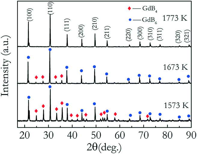
The XRD patterns of polycrystalline GdB6 rods prepared at different temperatures (Fig. 5) show that a suitable temperature is key, which can make the Gd metal completely melt and react with B powders. Otherwise, GdB4 impurities will form.
 |
| | Fig. 4 Preparation process of polycrystalline GdB6 by the SPS method. | |
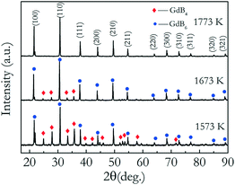 |
| | Fig. 5 XRD patterns of polycrystalline GdB6 at different sintering temperatures. | |
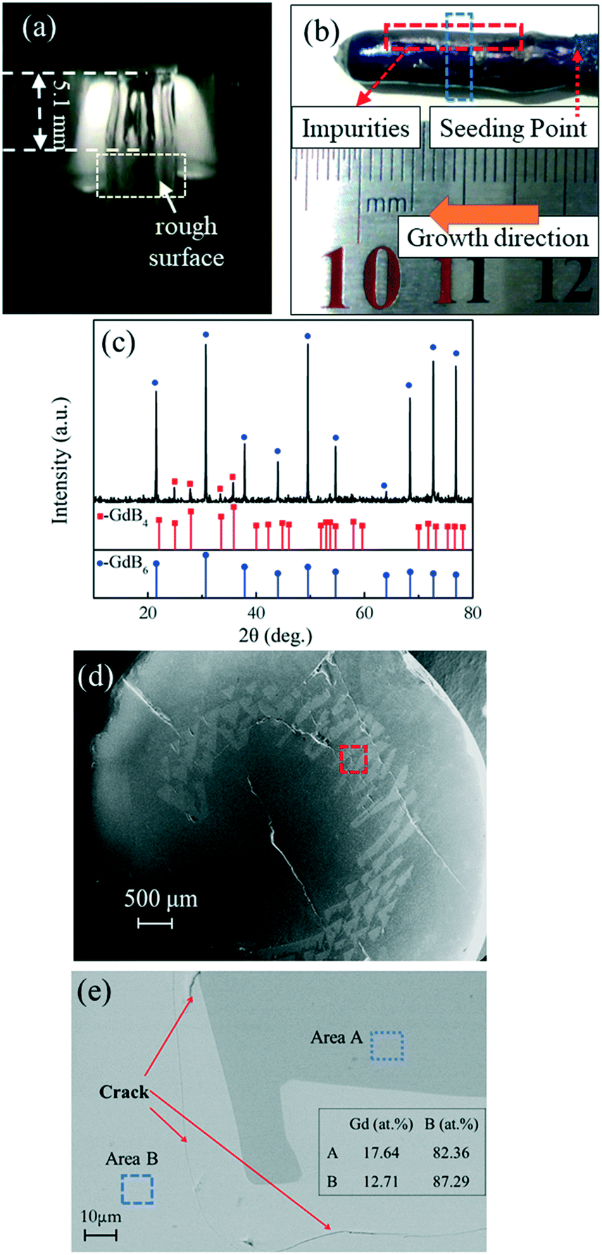
The biggest challenge in preparing a GdB6 single crystal by the optical floating-zone technique is how to avoid the formation of GdB4. Firstly, the preparation process of rare-earth hexaboride single crystals such as LaB6 and CeB6 is employed to grow the GdB6 single crystal, as presented in Table 1. It is prepared by a two-step process. A polycrystalline rod is firstly grown for purification with a growth rate of 20 mm h−1. For the second step, a growth rate of 8 mm h−1 is used to obtain the high-quality single crystal. The counter rotation rate between the feed and seed rods is 15 rpm. The growth atmosphere is Ar with high purity (≥99.999%). The total power of the lamps for stable crystal growth is 9.62 kW. However, it is found that the surface of the single crystal becomes rough during crystal growth because of irregular impurities making the surface look lacklustre (Fig. 6a). Silver-grey impurities are observed in the exterior surface and the core of the as-grown crystal, respectively, as shown in Fig. 6b, d and e. The grey impurities are demonstrated to be the GdB4 phase by analysing the XRD patterns of the powders of the crushed crystal (Fig. 6c). From Fig. 6e, the EDS results (presented in atomic ratio) further prove that the impurities are the GdB4 phase. The microcracks around the GdB4 phase have a serious influence on the quality of the as-grown crystal. GdB4 forms at the beginning and middle parts. When the crystal growth ends, B is enriched at the end of the crystal, and GdB4 disappears. A further attempt is to increase the rate of rotation from 15 rpm to 30 rpm, but GdB4 impurities are still obvious.
Table 1 The process parameters for the GdB6 single crystal grown by optical zone melting
|
|
Growth rate |
Rotation rate |
Atmosphere |
Length of molten zone |
Lamp power |
| GdB6 crystal with GdB4 impurities |
First step: 20 mm h−1; second step: 8 mm h−1 |
15 rpm counter rotation rate between the feed and seed rods |
Argon (≥99.999%) |
5.1 mm |
9.62 kW |
| GdB6 single crystal without GdB4 impurities |
4.5 mm |
8.24 kW |
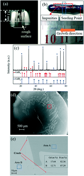 |
| | Fig. 6 (a) Photograph of the molten zone during the growth, (b) morphology, (c) XRD patterns of crushed powders, (d) secondary electron image from SEM and (e) backscattered electron image from SEM with EDS results (presented in atomic ratio) of the as-grown GdB6 crystal with impurities. The blue dotted lines in Fig. 6(b) indicate the part for the XRD and SEM measurements. The analysed area is indicated by red dotted lines in Fig. 6(d). The areas of EDS analysis are indicated by blue dotted lines in Fig. 6(e). | |
From Fig. 1, GdB6 will easily decompose into GdB4 and the liquid will be enriched with boron once the temperature of the melting zone is higher than 2780 K. In order to reduce the GdB4 phase as much as possible, suitable temperature and composition uniformity of the stable molten zone are necessary. To decrease the temperature of the molten zone and maintain the stabilization of the molten zone, strict control of the lamp power were carried out. Firstly, we carefully changed the position of the four lamps and reduced the spot size of the light source to as low as possible to shorten the length of the stable molten zone (Fig. 7a), which can decrease the diffusion path of the atoms and improve the composition uniformity of the molten zone. Meanwhile, the decrease in the spot size can increase the temperature of the molten zone since the light energy per unit area is higher. So, the light power can be further reduced to 8.24 kW under the premise that the molten zone is stable. The strict control of lamp power is very important to effectively limit the volatilization of the elements and ensure the stoichiometric composition of the compound. Studies showed that if the lamp power was increased to about 9 kW, GdB4 would form. Finally, the optimized growth conditions for the GdB6 single crystal are listed in Table 1.
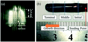 |
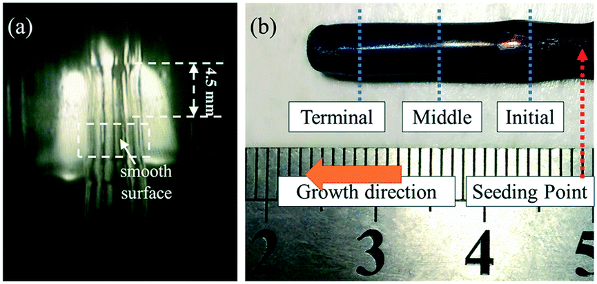
| | Fig. 7 (a) Photograph of the molten zone during the growth and (b) morphology of the as-grown GdB6 single crystal. The growth direction and the seeding point are presented. The blue dotted lines indicate the parts for the SEM and ICP measurements. | |
Characterization of the single crystal
As shown in Fig. 7, a smooth surface of the GdB6 single crystal is formed (Fig. 7a), and the as-grown GdB6 single crystal 25 mm in length and 5 mm in diameter is successfully prepared (Fig. 7b). The sample is purple blue and no impurity is observed on the surface.
The elemental content at different parts of the as-grown single crystal is shown in Table 2. The ratio of B/Gd = 4.93 at the initial part of the sample. After stable growth, the ratios of B/Gd are 5.77 and 5.82, respectively, which are very close to the theoretical value of B/Gd = 6, indicating that only a GdB6 single crystal (GdB5.77 and GdB5.82) forms. The SEM images of the transverse section of different parts of the as-grown GdB6 single crystal, corresponding to the ICP measurements, are presented in Fig. 8a–c. Some GdB4 impurities and cracks are observed in the core of the crystal at the beginning while at the middle and terminal parts, there are no impurity phases, cracks and defects. GdB4 impurities only form at the initial stage of crystal growth because of the unstable composition in the melting zone. When the melting zone becomes stable, the pure GdB6 single crystal is obtained.
Table 2 Content of gadolinium and boron measured by ICP-MS
| Element |
Initial part |
Middle part |
Terminal part |
| Gd |
70.02 μg mL−1 |
42.72 μg mL−1 |
60.42 μg mL−1 |
| B |
24.03 μg mL−1 |
16.81 μg mL−1 |
23.92 μg mL−1 |
| Ratio of B and Gd |
4.93 |
5.77 |
5.82 |
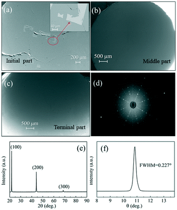 |
| | Fig. 8 (a)–(c) SEM images of the initial part, middle part and terminal part, (d) X-ray Laue diffraction photograph, (e) XRD patterns and (f) X-ray rocking curves of the GdB6 single crystal. | |
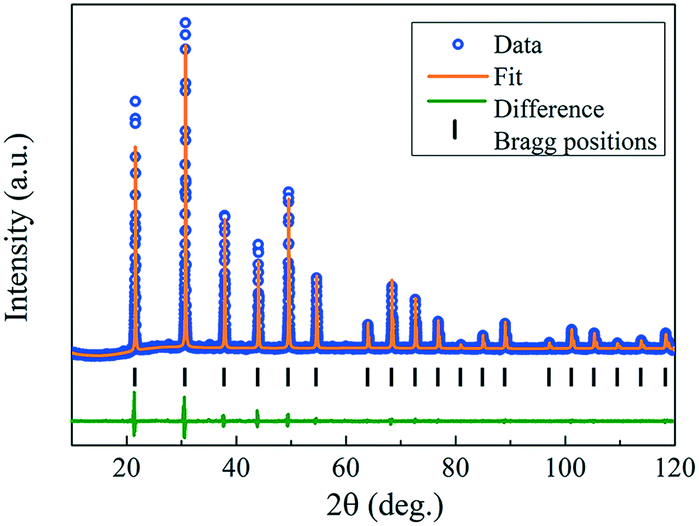
The crystal orientation of the GdB6 single crystal is characterized by X-ray Laue diffraction, as shown in Fig. 8b. The diffraction spot of the (100) crystal plane is in the center of the black circle, proving that the crystal orientation of the as-grown GdB6 single crystal is (100). The diffraction spots are independent, clear and have no splitting, which shows that the as-grown GdB6 has a good quality. The XRD pattern of the transverse section of the single crystal also shows that only the characteristic peaks of a GdB6 single crystal with (100), (200), and (300) are identified, and no other phase is detected (Fig. 8c). The full width at half-maximum (FWHM) of the X-ray rocking curves is usually used to evaluate the quality of the crystal, and a lower value of the FWHM represents a lower dislocation density of the as-grown crystal. A FWHM value of 0.227° for the GdB6 single crystal indicates that its dislocation density is very low (Fig. 8d). Rietveld refinement of the XRD data measured on the powders obtained from crushed single crystals was carried out using the GSAS-II program. As shown in Fig. 9, the lattice parameters obtained are a = b = c = 4.1096(4) Å and α = β = γ = 90° with the space group Pm![[3 with combining macron]](https://www.rsc.org/images/entities/char_0033_0304.gif) m (2θ range, 10–120°; GOF = 2.16; Rwp = 3.897%; RF = 3.69%; RF2 = 6.278%), which are in agreement with previous structural data.3,31,32
m (2θ range, 10–120°; GOF = 2.16; Rwp = 3.897%; RF = 3.69%; RF2 = 6.278%), which are in agreement with previous structural data.3,31,32
 |
| | Fig. 9 Rietveld refinement results of XRD data measured on the powders obtained from the crushed as-grown GdB6 single crystals. | |
Thermionic emission properties
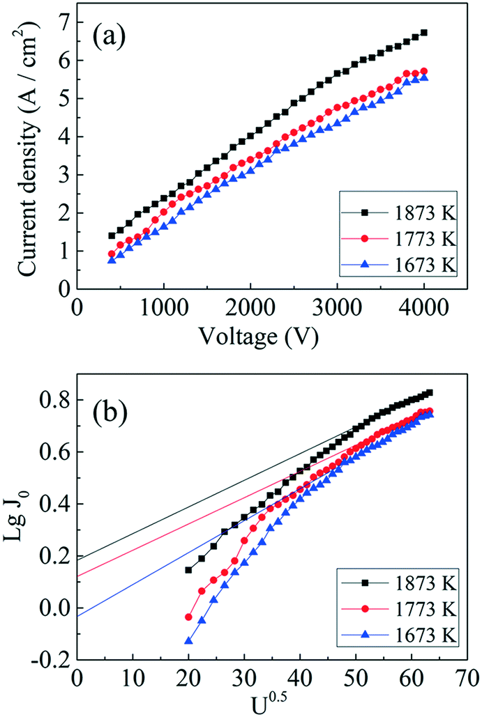
Fig. 10a shows the current density of the GdB6 single crystal tested at applied voltages U = 300 V up to 4000 V and various cathode temperatures from 1673 K to 1873 K. The largest current density is 6.73 A cm−2 at U = 4000 V and T = 1873 K. The cathode was cut from the middle part of the GdB6 single crystal.
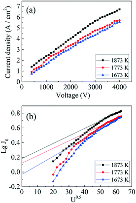 |
| | Fig. 10 (a) Thermionic emission properties and (b) Schottky curves of the GdB6 cathode at different temperatures. | |
The relationship between the effective work function Φe and thermionic emission current density can be described by the Richardson–Dushman equation:33
where
k is the Boltzmann constant,
k = 8.62 × 10
−5 eV K
−1,
A = 120.4 A cm
−2 K
−2, and
J0 is the zero-field current density and obtained from the Schottky equation:
34| | Lg![[thin space (1/6-em)]](https://www.rsc.org/images/entities/char_2009.gif) J = LgJ0 + 0.192U0.5T−1 J = LgJ0 + 0.192U0.5T−1 | (4) |
According to eqn (4), J0 can be obtained at U0.5 = 0, as shown in Fig. 10b. J0 is calculated to be 0.92 A cm−2 at 1673 K, 1.32 A cm−2 at 1773 K, and 1.52 A cm−2 at 1873 K, respectively, and the corresponding work functions of GdB6 are 2.84 eV at 1673 K, 2.98 eV at 1773 K, and 3.14 eV at 1873 K, respectively. The average work function of GdB6 is 2.99 eV, which is much lower than those from previous research studies,14–17 indicating that the pure GdB6 single crystals grown by the improved process have higher emission properties.
Theoretical calculation of the work function
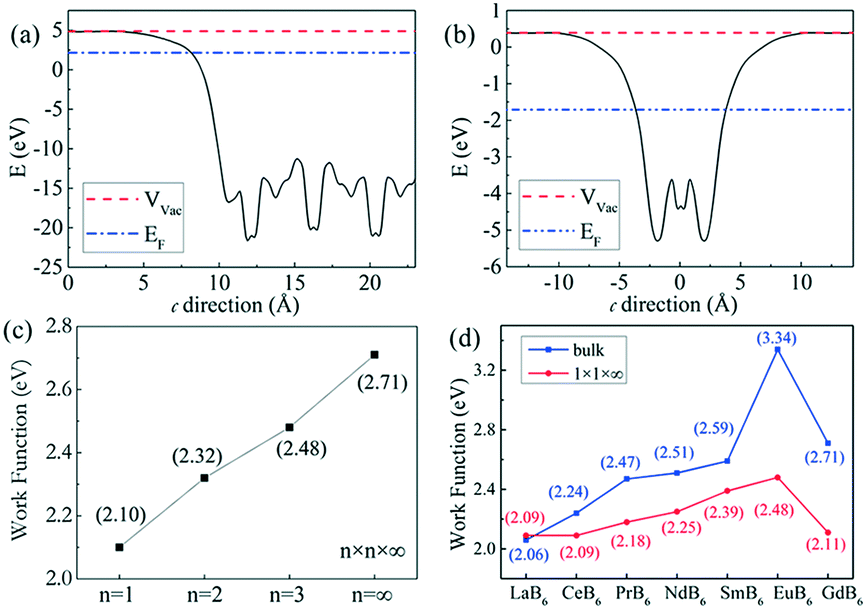
First-principles calculation is used to explain the wide difference between GdB6 single crystals with different sizes, and the work function can be written as:30where Vvac is the average potential in the vacuum of the cathode emission system, and EF is the Fermi energy level of the cathode emission system. The calculated electrostatic potentials of the (100) surface of the bulk and nanowire GdB6 along the c axis are shown in Fig. 11a and b. In the vacuum far away from the surface, the potential energy curves turn into flat straight lines rapidly, indicating the potential converging to the vacuum value. The work functions of bulk and nanowire GdB6 calculated by eqn (5) are 2.71 and 2.11 eV, respectively. GdB6 with a nanostructure does have a lower work function. To evaluate the influence of the size effect, the work function of nanowire GdB6 with n × n × ∞ (n = 1, 2, 3) is calculated, as shown in Fig. 11c. The work function monotonically increases as a function of n. When n tends to be infinite, the model is equivalent to that of the bulk structure, and the work function will gradually converge and approach the value of bulk GdB6.
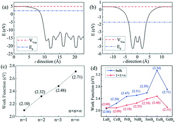 |
| | Fig. 11 Calculated electrostatic potential energy of the (100) surface of (a) bulk and (b) nanowire GdB6. Work function of bulk and n × n × ∞ (n = 1, 2, and 3) nanowires of (c) GdB6 and (d) rare earth hexaborides. | |
The calculated work function of 2.71 eV for the bulk GdB6 single crystal is lower than the experimental value of 2.99 eV because the GGA method may overestimate the spatial extension of conducting bands, leading to some differences between the calculated and experimental results.33 To make a comparison, we calculated the work function of other rare earth hexaborides, as shown in Fig. 11d. A relatively high work function compared to those of the rare earth hexaboride family belongs to the bulk GdB6 single crystal, while the nanostructure presents a lower work function, which is consistent with previous experimental studies.11–13
Conclusions
In summary, pure GdB6 single crystals with high quality are grown by the optical float zone method. GdB4 impurities can be effectively avoided by strictly controlling the lamp power. The single crystal with the (100) surface is confirmed to have high quality by X-ray diffraction and X-ray Laue diffraction. The thermionic emission experiment presents the largest current density of 6.73 A cm−2 and the average work function of GdB6 is 2.99 eV. The first-principles calculations show that the work function of the single crystal is obviously affected by the size effect, and the work function of the GdB6 single crystal is relatively high compared to those of the rare earth hexaboride family.
Conflicts of interest
There are no conflicts of interest to declare.
Acknowledgements
This work is supported by the National Natural Science Foundation of China (No. 51501051), the Joint Foundation of China's Ministry of Education in the Equipment Pre-Research (No. 6141A02022251) and the Fundamental Research Funds for the Central Universities (No. JZ2019HGTB0081).
References
- S. Xu, F. Jia, Y. Yang, L. Qiao, S. Hu, D. J. Singh and W. Ren, Interplay of Electronic, Phys. Rev. B, 2019, 100, 104408 CrossRef CAS.
- H. Hacker, J. Y. Shimada and K. S. Chung, Phys. Status Solidi A, 1971, 4, 459–465 CrossRef CAS.
- S. E. Luca, M. Amara, R. M. Galéra, F. Givord, S. Granovsky, O. Isnard and B. Beneu, Phys. B, 2004, 50, 39–42 CrossRef.
- M. Amara, S. E. Luca, R.-M. Galéra, F. Givord, C. Detlefs and S. Kunii, Phys. Rev. B: Condens. Matter Mater. Phys., 2005, 72, 064447 CrossRef.
- M. Anisimov, V. Glushkov, A. Bogach, S. Demishev, N. Samarin, A. Samarin, N. Shitsevalova, A. Levchenko, V. Filipov, S. Gábani, K. Flachbart and N. Sluchanko, Acta Phys. Pol., A, 2017, 131, 973–975 CrossRef CAS.
- K. Kuwahara, S. Sugiyama, K. Iwasa, M. Kohgi, M. Nakamura, Y. Inamura, M. Arai and S. Kunii, Appl. Phys. A: Mater. Sci. Process., 2002, 74, 302–304 CrossRef.
- L. Xiao, Y. Su, J. Ran, Y. Liu, W. Qiu, J. Wu, F. Lu, F. Shao, D. Tang and P. Peng, J. Appl. Phys., 2016, 119, 164903 CrossRef.
- X. H. Ji, Q. Y. Zhang, J. Q. Xu and Y. M. Zhao, Prog. Solid State Chem., 2011, 39, 51–69 CrossRef CAS.
- S. R. Suryawanshi, N. Kanhe, V. L. Mathe, D. M. Phase, D. J. Late and M. A. More, ChemistrySelect, 2017, 2, 562–566 CrossRef CAS.
- E. S. Zhukova, B. P. Gorshunov, G. A. Komandin, L. N. Alyabyeva, A. V. Muratov, Yu. A. Aleshchenko, M. A. Anisimov, N. Yu. Shitsevalova, S. E. Polovets, V. B. Filipov, V. V. Voronov and N. E. Sluchanko, Phys. Rev. B, 2019, 100, 104302 CrossRef CAS.
- H. Zhang, Q. Zhang, G. Zhao, J. Tang, O. Zhou and L. C. Qin, J. Am. Chem. Soc., 2005, 127, 13120 CrossRef CAS.
- S. R. Suryawanshi, A. K. Singh, M. Deo, D. J. Late, S. Sinha and M. A. More, CrystEngComm, 2015, 17, 3936–3944 RSC.
- K. K. Yadav, M. Sreekanth, Ankush, S. Ghosh and M. Jha, CrystEngComm, 2020, 22, 5473–5480 RSC.
- E. K. Storms and B. A. Mueller, J. Appl. Phys., 1981, 52, 2966–2970 CrossRef CAS.
- K. Ostrovskii, A. A. Taran, A. V. Kovalev, V. F. Tkachenko, E. M. Dudnik and A. A. Matvienko, Powder Metall. Met. Ceram., 1990, 29, 237–240 CrossRef.
- V. I. Lazorenko, N. I. Siman, A. I. Dmitriev and V. B. Muratov, Powder Metall. Met. Ceram., 1989, 28, 555–559 CrossRef.
- T. Tanaka, R. Nishitani, C. Oshima, E. Bannai and S. Kawai, J. Appl. Phys., 1980, 51, 3877–3883 CrossRef CAS.
- E. K. Storms, J. Appl. Phys., 1981, 52, 2961–2965 CrossRef CAS.
- S. G. Ebbinghaus, H. Krause and F. Syrowatka, Cryst. Growth Des., 2013, 13, 2990–2994 CrossRef CAS.
- Y. Wang, X. Yang, S. Ning, J. Zhao, B. Xu and J. Zhang, Vacuum, 2019, 165, 157–162 CrossRef CAS.
- S. Y. Ning, T. Iitaka, D. D. Xu, Z. Li, Y. Wang, X. Y. Yang and J. X. Zhang, Phys. Status Solidi A, 2019, 216, 1800706 CrossRef.
- Md. M. Hossain, S. Watauchi, M. Nagaoa and I. Tanaka, CrystEngComm, 2014, 16, 4619–4623 RSC.
- Y. B. Paderno, V. I. Lazorenko, N. I. Buryak, A. V. Kovalev, A. A. Matvienko and A. P. Galasun, Powder Metall. Met. Ceram., 1983, 22, 50–53 CrossRef.
- E. F. Westrum, J. T. S. Andrews, B. H. Justice and D. A. Johnson, J. Chem. Thermodyn., 2002, 34, 239–250 CrossRef CAS.
- K. Takahashi and S. Kunii, J. Solid State Chem., 1997, 133, 198–200 CrossRef CAS.
- I. Mazilu, M. Frontzek, W. Löser, G. Behr, A. Teresiak and L. Schultz, J. Cryst. Growth, 2005, 275, 103–107 CrossRef.
- S. M. Koohpayeh, D. Fort, A. Bradshaw and J. S. Abell, J. Cryst. Growth, 2009, 311, 2513–2518 CrossRef CAS.
- Q.-Y. Liu, Z.-Y. Liu, X.-B. Zhou, Z.-G. Liu, M.-X. Huo, X.-J. Wang and Y. Sui, Cryst. Growth Des., 2019, 19, 730–736 CrossRef CAS.
- Y.-C. Lai, G.-J. Shu, W.-T. Chen, C.-H. Du and F.-C. Chou, J. Cryst. Growth, 2015, 413, 100–104 CrossRef CAS.
- M. A. Uijttewaal, G. A. de Wijs and R. A. de Groot, J. Phys. Chem. B, 2006, 110, 18459–18465 CrossRef CAS.
- K. Sugiyama, Y. Koyoshi, S. Kunii, T. Kasuya and M. Date, J. Phys. Soc. Jpn., 1988, 57, 1762–1770 CrossRef CAS.
- Y. Takahashi, M. Fujimoto, M. Tsuchiko and K.-I. Ohshima, J. Appl. Crystallogr., 2001, 34, 208–209 CrossRef CAS.
- S. Y. Ning, T. Iitaka, X. Y. Yang, Y. Wang, J. J. Zhao, Z. Li and J. X. Zhang, J. Alloys Compd., 2018, 760, 1–5 CrossRef CAS.
- Y. Wang, J. X. Zhang, X. Y. Yang, Z. W. Zhu, J. J. Zhao, B. Xu and Z. Li, J. Alloys Compd., 2018, 769, 706–712 CrossRef CAS.
|
| This journal is © The Royal Society of Chemistry 2020 |
Click here to see how this site uses Cookies. View our privacy policy here. 
 *ab,
Yan
Wang
ab,
Zhongwen
Zhu
ab and
Jiuxing
Zhang
*ab
*ab,
Yan
Wang
ab,
Zhongwen
Zhu
ab and
Jiuxing
Zhang
*ab