
 Open Access Article
 This Open Access Article is licensed under a
 Creative Commons Attribution 3.0 Unported Licence
Effect of temperature and exfoliation time on the properties of chemically exfoliated MoS2 nanosheets†
Iwona
Janica
 abc,
Daniel
Iglesias
c,
Stefano
Ippolito
c,
Artur
Ciesielski
*bc and
Paolo
Samorì
*c
abc,
Daniel
Iglesias
c,
Stefano
Ippolito
c,
Artur
Ciesielski
*bc and
Paolo
Samorì
*c
aFaculty of Chemistry, Adam Mickiewicz University in Poznań, Uniwersytetu Poznańskiego 8, 61-614 Poznań, Poland
bCentre for Advanced Technologies, Adam Mickiewicz University, Uniwersytetu Poznańskiego 10, 61-614 Poznań, Poland
cUniversité de Strasbourg, CNRS, ISIS, 8 allée Gaspard Monge, 67000 Strasbourg, France. E-mail: ciesielski@unistra.fr; samori@unistra.fr
First published on 20th November 2020
Abstract
A systematic investigation of the experimental conditions for the chemical exfoliation of MoS2 using n-butyllithium as intercalating agent has been carried out to unravel the effect of reaction time and temperature for maximizing the percentage of monolayer thick-flakes and achieve a control over the content of metallic 1T vs. semiconductive 2H phases, thereby tuning the electrical properties of ultrathin MoS2 few-layer thick films.
During the last 15 years two-dimensional (2D) materials have attracted great attention due to their exceptional electronic, mechanical, thermal and optical properties.1,2 Graphene represents the prototypical and most studied 2D material,3,4 yet the lack of a band gap jeopardizes its application in (opto)electronics.5 As a result, the interest in other layered 2D materials (2DMs) has progressively increased.1 Among them, 2D transition metal dichalcogenides (TMDs), which are composed of a layer of metal atoms (e.g. Mo, W or Re) sandwiched between two layers of chalcogenide atoms (e.g. S, Se, Te) arranged in 2D sheets, represent one of the most intriguing class of 2DMs. In particular, molybdenum disulphide (MoS2)6,7 holds unique properties which makes it a promising scaffold for applications in catalysis,8,9 sensing,10 drug delivery11,12 and (opto)electronic devices,13,14 which can be further modified using various organic compounds.15,16 Despite its many advantageous features and over a decade of intense research, there is still a lack of efficient techniques for MoS2 production in large quantities and good quality, which is required for a successful integration of such material in real-life applications.
The chosen production method and experimental conditions defines the number of layers, lateral size and crystallinity of ultrathin MoS2 flakes and consequently their various physical and chemical properties. Three strategies are promising for the mass production of one- and few-layer thick MoS2 nanosheets: (1) chemical vapor deposition (CVD) starting from molybdenum and sulfur precursors which are deposited onto appropriate substrates,17 (2) liquid-phase exfoliation of bulk MoS2 assisted by ultrasounds18,19 or shear forces,20 and (3) chemical exfoliation of MoS2 with alkali metals compounds, generally containing Li ions that intercalate the bulk material.7–9,11,13,14,21,22 Bottom-up CVD appears an ideal method to obtain large-area and high-quality ultrathin MoS2 films that can be potentially scaled-up and used in electronics, yet the synthesized material is typically deposited onto metallic surfaces and requires to be transferred onto other substrates (e.g. SiO2) for further studies and applications. Another disadvantage of CVD technique is the need of employing high temperatures as well as inert atmosphere, thus the production costs are relatively higher than solution-based methods.1 Therefore, top-down exfoliation approaches, such as sonication-assisted exfoliation of bulk MoS2 in organic solvents or water/surfactant solutions, represent a better choice when high quantity of 2D flakes are required. Nevertheless, a drawback of this exfoliation approach concerns the production of defective materials with rather small lateral sizes and low content of single layer nanosheets. Noteworthy, the performance of solution-processed materials generally falls several orders of magnitude lower that the equivalent devices based on CVD nanosheets.14
The chemical exfoliation process using lithium compounds, pioneered by Joensen et al.,23 leads to almost completely exfoliated materials, in terms of both yield and flake thickness (mostly 1–5 layers).24 This method is based on the intercalation of bulk MoS2 with lithium ions derived mainly from organolithium compounds, such as n-butyllithium (n-BuLi), that occasionally can be assisted by electrochemical process14 and subsequent sonication in aqueous solution of the intercalated product (LixMoS2), leading to stable colloidal dispersions of negatively charged chemically exfoliated MoS2 (ce-MoS2) nanosheets.25 This process also causes a conversion of the original semiconducting 2H phase (trigonal prismatic coordination) of MoS2 structure to the metallic 1T phase (octahedral coordination), that can be disadvantageous for electronic applications. However, since the 1T phase is 107 more conductive than 2H phase and displays additional reaction sites,26 it can surpass 2H phase for some applications such as catalysis9 or as an electrode for supercapacitors.26 Even though ce-MoS2 using n-BuLi as intercalating agent has been explored for many years, it suffers from the lack of systematic studies (Table S2 in ESI† shows a compilation of several described procedures). Hitherto, the intercalation reactions have been typically conducted for 2 days, although experiments carried out for 8 h,25 1 day21,27 or 3 days13 have also been reported. The temperature at which the chemical exfoliation has been performed varied from room temperature (RT)8 up to 100 °C.28 Different weight ratios of MoS2 and the intercalation agent have been employed, albeit n-BuLi is usually used in ∼2–3 equivalent excess per MoS2 formula unit. Noteworthy, establishing optimal protocols for the chemical exfoliation of MoS2 using n-BuLi as intercalating agent would enable to maximize the percentage of monolayer thick-flakes and their concentration as well as to control the ratio between the 2H and 1T phases, thereby making it possible not only to tune the properties of the exfoliated material, but also its reactivity, being key for its controlled functionalization.
In this work, we have investigated the effect of the reaction time (1–3 days) and temperature (RT and 55 °C) on the quality of produced ce-MoS2 using n-BuLi as an intercalating agent. In-depth multiscale microscopic, spectroscopic and electrical characterizations have been performed in order to study the chemical composition, the content of metallic 1T phase as well as the morphology and conductivity of the films prepared from the obtained ce-MoS2, with the ultimate goal of establishing the optimal conditions for an efficient chemical exfoliation process. Moreover, the transition from 1T to 2H phase achieved upon vacuum annealing made it possible to study of the electrical characteristics by fabricating field-effect transistor (FET) devices.
A detailed preparation of ce-MoS2 is described in the ESI.† Briefly, the mixture of MoS2 powder and n-BuLi solution in hexane (2.5 eq.) was stirred for 1, 2 or 3 days at RT as well as at elevated temperature. After the filtration, the collected solid was dispersed in water, sonicated for 1 h and then centrifugated. In the final step, the dispersion was dialyzed in order to remove residual of lithium compounds. Subsequently, specified amount of each solution was filtrated and the collected solid was dried and weighted in order to determine the concentration. The calculated concentration of the resulting dispersion was similar in all cases, i.e. ∼0.5 mg mL−1, however the solution obtained in 1 day reaction at RT exhibited the lowest value, i.e. ∼0.3 mg mL−1 (Fig. 1a). The thermogravimetric analyses revealed a noticeable decrease in weight during thermal annealing of the samples prepared at RT in 1 day (Fig. S1, ESI†) when compared to other samples. The analysis of the zeta potential provided similar results for all the tested reaction conditions showing no particular trend (Fig. S2, ESI†).
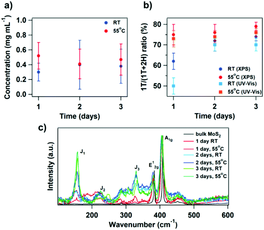 | ||
| Fig. 1 (a) Concentration of MoS2 dispersions after dialysis obtained as a result of experiment at room (blue) and elevated temperature (red), with the standard mean deviation expressed in the form of error bars; (b) 1T/1T + 2H ratio calculated based on high-resolution Mo3d XPS spectra (ESI† Fig. S1, blue and red) as well as UV-Vis spectra (ESI† Fig. S4 and eqn (S1), light blue and orange); (c) comparison of Raman spectrum obtained for bulk MoS2 (black) and exfoliated materials after reaction in various experimental conditions. | ||
The content of 1T vs. 2H phases represents one of the most important characteristics explored in the qualitative analysis of the exfoliated MoS2 nanosheets. The 1T/2H ratio was evaluated by XPS, UV-Vis and Raman spectroscopy. For the XPS and Raman characterization, the samples were prepared by a vacuum filtration and dry-transfer method (see ESI†). The content of each crystalline phase obtained at different reaction time and temperature is displayed in Fig. 1b. The 1T/2H ratio was calculated based on the area of 2H-MoS2 doublet at binding energies values ∼229.1 eV and ∼232.3 eV as well as the additional peaks shifted toward lower binding energies by ∼0.8 eV in relative to the 2H-MoS2 peaks doublets, which are assigned to 1T-MoS2 in the high-resolution XPS spectra the Mo3d region (Fig. S3, ESI†).14,21 The lowest content of 1T phase is observed in the material produced in 1 day reaction at RT with a value of ∼60%, while the highest content is close to 80% for the material generated in a 3 days lasting reaction at 55 °C. Noteworthy, the content of metallic phase for the remaining exfoliated MoS2 is similar and ranges between ∼70% and ∼80%. On the other hand, ce-MoS2 produced at 55 °C exhibits increased amount of 1T phase compared to samples prepared at same reaction duration at RT. These results are in good agreement with the phase analysis carried out by monitoring the S2p peak in high resolution XPS spectra (Fig. S4, ESI†). Moreover, the presence of MoO2 and MoO3, which is inherent to this chemical exfoliation method, appeared not to be influenced neither by temperature nor by the reaction time. In addition, as suggested by Knirsch et al.,21 the 1T/2H ratio can be also determined from UV-Vis spectra (eqn (S1) and Fig. S5, ESI†). Fig. 1b shows that the material produced in 1 day lasting reaction at RT possesses the lowest content of 1T phase, in agreement with XPS result. However, such absolute value is lower (∼50%) in the case of UV-Vis whereas the other results obtained with the latter technique are in good quantitative agreement with values determined from XPS measurements.
Further characterization of the exfoliated MoS2 was conducted by Raman spectroscopy. The Raman spectra displayed in Fig. 1c, can be used to track differences between the MoS2 bulk powder and ce-MoS2. Reference sample excited with green laser (λ = 532 nm) displayed two intense peaks at ∼383 cm−1 and ∼408 cm−1 that are attributed to E12g in-plane and A1g out-of-plane modes, respectively.29 Similar Raman spectrum is observed for samples obtained in a 1 day reaction at RT. However, the main E12g and A1g peaks are broaden and slightly shifted (∼380 cm−1 and ∼405 cm−1, respectively). On the other hand, three additional peaks at ∼156 cm−1, ∼227 cm−1 and ∼330 cm−1 are visible in the spectra of other exfoliated materials corresponding to J1, J2 and J3 modes, respectively, which are absent in bulk reference MoS2.14 The intensities of these peaks vary depending on the reaction conditions and are most pronounced in the samples resulting from a 3 days reaction at RT, 3 days at 55 °C as well as 2 days at 55 °C. The presence of these peaks (J1–J3) suggests that metallic 1T-MoS2 phase exists in the exfoliated materials.14,29 Moreover, the E12g and A1g peaks are broaden as well as shifted.
All these results showed significative differences between 1 day lasting reaction at RT and the other samples. To investigate the morphology as well as the statistical distribution of lateral size and thickness of ce-MoS2 atomic force microscopy (AFM) and scanning electron microscopy (STEM) imaging were carried out (Fig. S7 and S8, ESI†). The AFM analysis of spin-coated ce-MoS2 dispersions displayed the presence of nanoflakes with an average lateral size of ∼200 nm and thickness in the range of 3–5 nm. SEM imaging (Fig. 2) of films prepared by dry-transfer method revealed the presence of thick crystal-like flakes in films of ce-MoS2 (1 day, RT) demonstrating that the experimental condition employed for the exfoliation are insufficient for achieving ultrathin flakes (Fig. 2a). Conversely, uniform and homogenous films composed of well exfoliated ce-MoS2 nanosheets have been observed for materials prepared with reactions lasting 1 day at 55 °C and 2–3 days (both at RT and 55 °C) (Fig. 2b–f).
 | ||
| Fig. 2 SEM images and the conductivity (σ) of MoS2 films obtained after the exfoliation: (a) 1 day, RT; (b) 1 day, 55 °C; (c) 2 days, RT; (d) 2 days, 55 °C; (e) 3 days, RT; (f) 3 days, 55 °C. | ||
We extended out studies to the electrical characterization of as-prepared films. The sheet resistance was measured by four-point-probe set-up and the conductivity was calculated using eqn (S2) and (S3) (ESI†). Metals are good electrical conductors, thus materials with higher content of metallic 1T-MoS2 phase should display higher conductivities. The material produced in 1 day reaction at RT, being characterized by the smallest amount of 1T-MoS2 phase, exhibits the lowest conductivity, amounting to ∼102 S m−1. Conversely, all the MoS2 displayed very similar conductivities (insets in Fig. 2). On the other hand, the material produced in 1 day reaction at 55 °C was drop-casted onto prepatterned gold interdigitated electrodes on SiO2/Si substrates, to fabricate a bottom-contact/bottom-gate transistor (Fig. S10, ESI†). The output and transfer curves revealed no modulation with the applied gate voltage, indicating a predominance of the metallic phase in the electrical characteristics. The coverage of the electrodes by drop-casting was not very efficient, which made the analysis of the transport properties very challenging. To overcome this problem, ce-MoS2 (1 day, 55 °C) was deposited on SiO2/Si by dry-transfer process and the gold electrodes were evaporated on top (yielding a top-contact/bottom gate configuration). This method allowed the fabrication of continuous films with controlled thickness (Fig. S10, ESI†). The device was vacuum annealed at increasing temperatures from 50 to 300 °C. We observed a dramatic drop in the conductivity upon annealing at 50–200 °C, before reaching a plateau at 250 °C (Fig. 3a). This is due to the phase transition from 1T to 2H phase. Since it is well known that dielectrically-gated (solid-state) transistors based on TMDs show poor electrical performance (i.e. switching current < 10),18 top-contact/top-gate device were fabricated by exploiting EMIM-TFSI ionic liquid as liquid dielectric and a Pt wire as gate electrode. Noteworthy, the samples annealed at 300 °C exhibited semiconducting properties, in agreement with nearly completed phase transition from 1T to 2H-MoS2. Moreover, the devices displayed unipolar n-type behaviour characterized by a field-effect mobility (μFE) of 10−2 cm2 V−1 s−1 and ION/IOFF ratio of ∼10. The electrical performance is affected by the initial high degree of disorder associated to the 2H/1T nanoscale polymorphism as well as thermal evolution/expansion of defects generated during the intercalation/exfoliation process. The formation of 2H/1T boundaries following the rearrangement of 1T domains into 2H domains might represent the major limiting factor to high-performance devices.14 Nevertheless, the fabricated devices display performances close to the state-of-the-art for solution-processed TMDs,30 highlighting the importance of the research and the room for improvement.
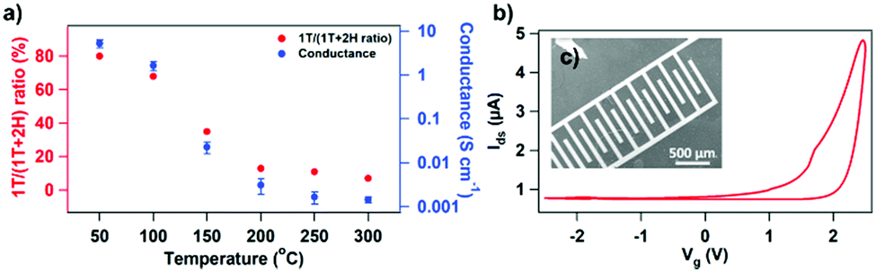 | ||
| Fig. 3 (a) Changing in the 1T/(1T + 2H) ratio (red) based on Mo3d spectra (Fig. S11, ESI†) and conductance (blue) with temperature; (b) transfer curve of ionic liquid gated FET device after annealing at 300 °C; (c) SEM image of the gold interdigitated electrodes evaporated on ce-MoS2 film. All analysis and measurements were performed on sample (1 day, 55 °C). | ||
In summary, we have performed a comparative study to unveil the effect of reaction time and temperature on the chemical exfoliation of MoS2 using n-BuLi as the intercalating agent. In-depth characterizations revealed that the lowest content of metallic 1T phase (∼50%) was obtained for reaction lasting for 1 day at RT. Our findings show that those commonly employed conditions are insufficient to allow the efficient exfoliation of monolayer thick MoS2. On the contrary, ce-MoS2 obtained in the reaction conducted at elevated temperature and/or for prolongated time was characterized by higher content of 1T phase (up to ∼80%). The high processability of such ce-MoS2 dispersions can be exploited for the preparation, upon thermal annealing conversion, of homogeneous 2H phase based semiconducting films for field-effect transistors. This study is of importance as it defines ad hoc experimental conditions to achieve an efficient chemical exfoliation of ultrathin MoS2 nanoflakes, paving the way for their further functionalization as promising strategy to optimize the properties for applications in (opto)electronics, catalysis or chemical sensing.
This work was financed by the Polish National Science Center (Grant No. 2019/35/B/ST5/01568) and by grant no. POWR.03.02.00-00-I023/17 co-financed by the EU through the European Social Fund under the Operational Program Knowledge Education Development. The activity in Strasbourg was supported by the EC through the ERC project SUPRA2DMAT (GA-833707) and the Graphene Flagship Core 3 project (GA-881603) as well as the Labex projects CSC (ANR-10LABX-0026 CSC) and NIE (ANR-11-LABX-0058 NIE) within the Investissement d’Avenir program ANR-10-IDEX-0002-02 and the International Center for Frontier Research in Chemistry.
Conflicts of interest
There are no conflicts to declare.Notes and references
- C. Tan, X. Cao, X.-J. Wu, Q. He, J. Yang, X. Zhang, J. Chen, W. Zhao, S. Han, G.-H. Nam, M. Sindoro and H. Zhang, Chem. Rev., 2017, 117, 6225–6331 CrossRef CAS.
- S. Witomska, T. Leydecker, A. Ciesielski and P. Samorì, Adv. Funct. Mater., 2019, 29, 1901126 CrossRef.
- K. S. Novoselov, A. K. Geim, S. V. Morozov, D. Jiang, Y. Zhang, S. V. Dubonos, I. V. Grigorieva and A. A. Firsov, Science, 2004, 306, 666–669 CrossRef CAS.
- A. H. Castro Neto, F. Guinea, N. M. R. Peres, K. S. Novoselov and A. K. Geim, Rev. Mod. Phys., 2009, 81, 109–162 CrossRef CAS.
- A. K. Geim and K. S. Novoselov, Nat. Mater., 2007, 6, 183 CrossRef CAS.
- M. Chhowalla, H. S. Shin, G. Eda, L.-J. Li, K. P. Loh and H. Zhang, Nat. Chem., 2013, 5, 263–275 CrossRef.
- G. Eda, T. Fujita, H. Yamaguchi, D. Voiry, M. Chen and M. Chhowalla, ACS Nano, 2012, 6, 7311–7317 CrossRef CAS.
- J. I. Paredes, J. M. Munuera, S. Villar-Rodil, L. Guardia, M. Ayán-Varela, A. Pagán, S. D. Aznar-Cervantes, J. L. Cenis, A. Martínez-Alonso and J. M. D. Tascón, ACS Appl. Mater. Interfaces, 2016, 8, 27974–27986 CrossRef CAS.
- R. Peng, L. Liang, Z. D. Hood, A. Boulesbaa, A. Puretzky, A. V. Ievlev, J. Come, O. S. Ovchinnikova, H. Wang, C. Ma, M. Chi, B. G. Sumpter and Z. Wu, ACS Catal., 2016, 6, 6723–6729 CrossRef CAS.
- J. Zhao, N. Li, H. Yu, Z. Wei, M. Liao, P. Chen, S. Wang, D. Shi, Q. Sun and G. Zhang, Adv. Mater., 2017, 29, 1702076 CrossRef.
- T. Liu, C. Wang, W. Cui, H. Gong, C. Liang, X. Shi, Z. Li, B. Sun and Z. Liu, Nanoscale, 2014, 6, 11219–11225 RSC.
- T. Liu, C. Wang, X. Gu, H. Gong, L. Cheng, X. Shi, L. Feng, B. Sun and Z. Liu, Adv. Mater., 2014, 26, 3433–3440 CrossRef CAS.
- A. L. Santhosha, P. K. Nayak, K. Pollok, F. Langenhorst and P. Adelhelm, J. Phys. Chem. C, 2019, 123, 12126–12134 CrossRef CAS.
- M. El Garah, S. Bertolazzi, S. Ippolito, M. Eredia, I. Janica, G. Melinte, O. Ersen, G. Marletta, A. Ciesielski and P. Samorì, FlatChem, 2018, 9, 33–39 CrossRef CAS.
- M. Vera-Hidalgo, E. Giovanelli, C. Navío and E. M. Pérez, J. Am. Chem. Soc., 2019, 141, 3767–3771 CrossRef CAS.
- A. Stergiou and N. Tagmatarchis, Chem. – Eur. J., 2018, 24, 18246–18257 CrossRef CAS.
- S.-Y. Kim, J. Kwak, C. V. Ciobanu and S.-Y. Kwon, Adv. Mater., 2019, 31, 1804939 CrossRef.
- G. Cunningham, M. Lotya, C. S. Cucinotta, S. Sanvito, S. D. Bergin, R. Menzel, M. S. P. Shaffer and J. N. Coleman, ACS Nano, 2012, 6, 3468–3480 CrossRef CAS.
- J. N. Coleman, M. Lotya, A. O’Neill, S. D. Bergin, P. J. King, U. Khan, K. Young, A. Gaucher, S. De, R. J. Smith, I. V. Shvets, S. K. Arora, G. Stanton, H.-Y. Kim, K. Lee, G. T. Kim, G. S. Duesberg, T. Hallam, J. J. Boland, J. J. Wang, J. F. Donegan, J. C. Grunlan, G. Moriarty, A. Shmeliov, R. J. Nicholls, J. M. Perkins, E. M. Grieveson, K. Theuwissen, D. W. McComb, P. D. Nellist and V. Nicolosi, Science, 2011, 331, 568–571 CrossRef CAS.
- S. Biccai, S. Barwich, D. Boland, A. Harvey, D. Hanlon, N. McEvoy and J. N. Coleman, 2D Mater., 2018, 6, 015008 CrossRef.
- K. C. Knirsch, N. C. Berner, H. C. Nerl, C. S. Cucinotta, Z. Gholamvand, N. McEvoy, Z. Wang, I. Abramovic, P. Vecera, M. Halik, S. Sanvito, G. S. Duesberg, V. Nicolosi, F. Hauke, A. Hirsch, J. N. Coleman and C. Backes, ACS Nano, 2015, 9, 6018–6030 CrossRef CAS.
- R. Zeng, Z. Li, L. Li, Y. Li, J. Huang, Y. Xiao, K. Yuan and Y. Chen, ACS Sustainable Chem. Eng., 2019, 7, 11540–11549 CrossRef CAS.
- P. Joensen, R. F. Frindt and S. R. Morrison, Mater. Res. Bull., 1986, 21, 457–461 CrossRef CAS.
- M. Samadi, N. Sarikhani, M. Zirak, H. Zhang, H.-L. Zhang and A. Z. Moshfegh, Nanoscale Horiz., 2018, 3, 90–204 RSC.
- Y. Liang, H. D. Yoo, Y. Li, J. Shuai, H. A. Calderon, F. C. Robles Hernandez, L. C. Grabow and Y. Yao, Nano Lett., 2015, 15, 2194–2202 CrossRef CAS.
- M. Acerce, D. Voiry and M. Chhowalla, Nat. Nanotechnol., 2015, 10, 313–318 CrossRef CAS.
- D. Iglesias, S. Ippolito, A. Ciesielski and P. Samorì, Chem. Commun., 2020, 56, 6878–6881 RSC.
- K. Pramoda, U. Gupta, M. Chhetri, A. Bandyopadhyay, S. K. Pati and C. N. R. Rao, ACS Appl. Mater. Interfaces, 2017, 9, 10664–10672 CrossRef CAS.
- L. Yuwen, H. Yu, X. Yang, J. Zhou, Q. Zhang, Y. Zhang, Z. Luo, S. Su and L. Wang, Chem. Commun., 2016, 52, 529–532 RSC.
- A. G. Kelly, T. Hallam, C. Backes, A. Harvey, A. S. Esmaeily, I. Godwin, J. Coelho, V. Nicolosi, J. Lauth, A. Kulkarni, S. Kinge, L. D. A. Siebbeles, G. S. Duesberg and J. N. Coleman, Science, 2017, 356, 69–73 CrossRef CAS.
Footnote |
| † Electronic supplementary information (ESI) available. See DOI: 10.1039/d0cc06792j |
| This journal is © The Royal Society of Chemistry 2020 |