
 Open Access Article
 This Open Access Article is licensed under a Creative Commons Attribution-Non Commercial 3.0 Unported Licence
Semi-transparent quaternary oxynitride photoanodes on GaN underlayers†
Zili
Ma
 ab,
Karolina
Piętak
cd,
Jędrzej
Piątek
b,
Justin
Reed DeMoulpied
e,
Anna
Rokicińska
f,
Piotr
Kuśtrowski
f,
Richard
Dronskowski
ag,
Sebastian
Zlotnik
ch,
Robert H.
Coridan
*e and
Adam
Slabon
*b
ab,
Karolina
Piętak
cd,
Jędrzej
Piątek
b,
Justin
Reed DeMoulpied
e,
Anna
Rokicińska
f,
Piotr
Kuśtrowski
f,
Richard
Dronskowski
ag,
Sebastian
Zlotnik
ch,
Robert H.
Coridan
*e and
Adam
Slabon
*b
aInstitute of Inorganic Chemistry, RWTH Aachen University, 52056 Aachen, Germany
bDepartment of Materials and Environmental Chemistry, Stockholm University, 10691 Stockholm, Sweden. E-mail: adam.slabon@mmk.su.se
cŁukasiewicz Research Network, Institute of Electronic Materials Technology, Wolczynska 133, 01-919 Warsaw, Poland
dWarsaw University of Technology, Faculty of Chemistry, Noakowskiego 3, 00-664 Warsaw, Poland
eDepartment of Chemistry and Biochemistry and the Materials Science and Engineering Program, University of Arkansas, Fayetteville, Arkansas 72701, USA. E-mail: rcoridan@uark.edu
fFaculty of Chemistry, Jagiellonian University, Gronostajowa 2, 30-387 Krakow, Poland
gHoffmann Institute of Advanced Materials, Shenzhen Polytechnic, 7098 Liuxian Boulevard, Nanshan District, Shenzhen, China
hInstitute of Applied Physics, Military University of Technology, 2 Kaliskiego Str., 00-908 Warsaw, Poland
First published on 29th September 2020
Abstract
Conformal atomic layer deposition (ALD) technique is employed to make semi-transparent TaOxNy, providing the possibility to build semi-transparent oxy(nitride) heterojunction photoanodes on conductive substrates. A generalized approach was developed to manufacture semi-transparent quaternary metal oxynitrides on conductive substrates beyond semi-transparent binary Ta3N5 photoanodes aiming for wireless tandem photoelectrochemical (PEC) cells.
A sustainable solution for storing the solar energy in principle can be achieved by PEC technology, which is based on splitting of earth-abundant water into the renewable energy carrier hydrogen and oxygen.1 Connecting the photoanode and the photocathode in a stacked configuration enables the devices to maximize sunlight harvesting by using narrow band gap semiconductors in tandem.2 Thus, the photovoltage generated in each photoabsorber can be summed to drive water splitting at high efficiency. In the tandem geometry, the photoanode as first photoelectrode absorbs photons of higher energy while the photocathode absorbs the transmitted photons to drive water reduction.3 Fig. S1 (ESI†) depicts a wireless tandem PEC cell configuration, in which the solar photons not absorbed by the semi-transparent photoelectrode at the front side will pass through the intermediate transparent conductive substrate (TCS). Subsequently, the remaining photons can be harvested by the second photoelectrode with a smaller band gap energy (Eg).4
Additionally, the other advantages of the wireless PEC tandem cell are the (i) flexibility in materials selection, (ii) low resistance losses and (iii) high proton conductivity,5,6 which target for high solar-to-hydrogen (STH) conversion efficiency.7 Furthermore, the wireless configuration is more suitable for industrial manufacturing in comparison to the wired tandem configuration in which the photoabsorbers are connected via an external circuit.8 With respect to the TCS materials required for a PEC tandem cell, the most commonly used substrates are transparent conductive oxides (TCOs) such as fluorine/indium doped tin oxide (FTO/ITO) and aluminum doped zinc oxide (AZO).9 These TCS materials, however, cannot be applied to materials that require synthetic conditions including ammonia at elevated temperatures (>873 K). As such, common TCS materials are limited in their implantation for nitrogen-containing photoelectrode materials.10,11
For commercialization of PEC technology, it is widely accepted that the STH efficiency needs to be greater than 10%.12 Among the often studied metal oxide-based photoanodes such as TiO2, WO3, ZnFe2O4, BiVO4, the most representative one is the latter,13 exhibiting the highest STH conversion efficiency of 3.7% in a bias-free tandem cell for PEC water splitting.7 To achieve higher STH efficiency, the front photoanode in wireless tandem PEC cells has to be semi-transparent. Thus, it must absorb photons with energy larger than its band gap and transmit the remaining photons to the photocathode behind it, avoiding scattering or parasitic absorption of the transmitted light.
Metal nitrides, oxynitrides and N-doped oxides exhibit narrower band gaps than the best-performing oxidic photoanode candidates. An example is Ta3N5 with a bandgap of 2.1 eV and that can be obtained by ammonolysis of Ta2O5. This synthetic approach makes it challenging to produce semi-transparent metal (oxy)nitrides on FTO, because the transparent SnOx becomes metallic Sn under the nitridation conditions.14 It should be noted that fabrication of semi-transparent photoanodes by means of electrophoretic deposition of powder samples displays significant worse mechanical stability under operating conditions. Recently, the groups of Hamann10,14 and Domen15–17 have demonstrated alternative methods to fabricate semi-transparent Ta3N5 photoanodes. Although semitransparent films of Ta3N5 can reach 6.3 mA cm−2 at 1.23 V vs. reversible hydrogen electrode (RHE),17 the material suffers from a high onset potential of 0.3–0.8 V vs. RHE,14,18,19 which then must be generated by the tandem photocathode for overall water splitting to occur.20
The quaternary metal oxynitrides ATa(O,N)3 display a photocurrent onset at smaller applied potentials and, for several compounds, can potentially exhibit a higher theoretical STH efficiency than the binary Ta3N5.21,22 This is due to the narrower band gaps of quaternary metal oxynitrides, depending on the chemical composition and being tunable within the range of 1.7 and 2.4 eV.22–24 This renders semi-transparent quaternary metal oxynitrides generally as very promising photoanode candidates for PEC tandem cells, which could outperform Ta3N5-based devices. So far, semi-transparent quaternary metal oxynitride films have been mainly fabricated by means of reactive radiofrequency (RF) magnetron sputtering25–28 or pulsed laser deposition (PLD)29,30 on MgO or Nb:SrTiO3 substrate. In case of the RF approach, the oxynitride sputtering targets have to be made first with multi-step processes, and harsh conditions (usually up to 1073 K for film deposition) are required, too.27 The development of photoelectrode materials with more narrow band gaps than Ta3N5 and hematite is mainly motivated by the higher theoretical light absorption capacity.11 Recently, Domen et al. have demonstrated a core–shell heterojunction photoanode of Ta3N5-nanorods/BaTaO2N, generating a stable photocurrent owing to efficient generation and extraction of charge carriers.31 For the reproducible fabrication of thin films exhibiting controllable thickness on the atomic scale and conformal features, Atomic Layer Deposition (ALD) is a promising technique for the deposition of oxidic precursor layers for subsequent nitridation.32
In this communication, we demonstrate the synthesis of semi-transparent quaternary photoanodes on the examples of SrTaO2N and LaTiO2N. First, ALD was explored to obtain semi-transparent TaOxNy thin films on conductive n-type GaN substrate. GaN was selected as the substrate, because it can maintain chemical stability at high temperature in NH3 without degradation15 and under ambient conditions.33 Low pressure metalorganic vapor phase epitaxy reactor (MOVPE) was employed to grow unintentionally-doped GaN epitaxial film on double-sided polished Al2O3 (sapphire) substrates (see ESI†).
The ALD cycle procedure for Ta2O5 deposition is illustrated in Fig. 1 (see ESI†). Nitridation at 1148 K for 2 h converted the Ta2O5 to TaOxNy, i.e. N-doped Ta2O5, which was confirmed by X-ray photoelectron spectroscopy (XPS) (Fig. S2, see ESI† for experimental details). It has been reported that ammonolysis of Ta2O5 at higher temperatures may yield the binary Ta3N5.34 The transmittance of the prepared thin film was evaluated by means of Ultraviolet-visible spectroscopy (UV-vis) as a function of the wavelength (Fig. 2a). After depositing Ta2O5 onto Al2O3/GaN substrate, the transmittance only decreased slightly because of thin Ta2O5 layer and its wide band gap. After nitridation, the transmittance of the resulting Al2O3/GaN/TaOxNy thin film decreased to around 70% at wavelengths above 600 nm.
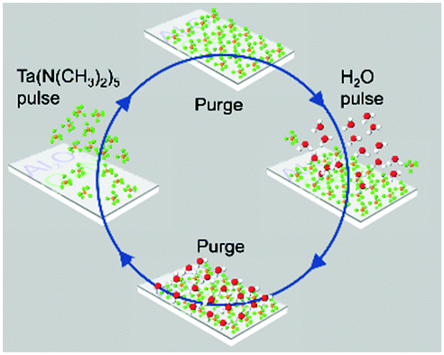 | ||
| Fig. 1 Scheme of ALD procedure for Ta2O5 on substrate. | ||
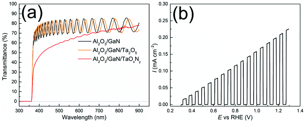 | ||
| Fig. 2 (a) UV-vis transmittance spectra. (b) LSV of corresponding Al2O3/GaN/TaOxNy photoanode measured in 0.1 M NaOH under chopped AM 1.5G illumination (1 sun, 100 mW cm−2). | ||
The light-absorbing thin film TaOxNy on the Al2O3/GaN substrate was composed of grains with approximately size of 100 nm due to sintering at high temperature substrate as observed by scanning electron microscopy (SEM) (Fig. S3 in the ESI†). The grains are distributed uniformly throughout the substrate as observed at the SEM micrograph (Fig. S4, ESI†). The Al2O3/GaN/TaOxNy photoanode, which was prepared by MOVPE and ALD, generated a photocurrent of 0.21 mA cm−2 at 1.23 V vs. RHE in 0.1 M NaOH under AM 1.5G illumination (1 sun) as shown in the linear sweep voltammetry curve (LSV, Fig. 2b). The photocurrent is lower than other reported semi-transparent Ta3N5 film because of smaller thickness and smaller amount of N incorporation.15–17 The photocurrent maintained stable during chronoamperometry (CA) (Fig. S5, ESI†).
Given the suitability of the deposited GaN layer for electron transport of nitridic light absorbers, we elucidated the possibility to fabricate quaternary metal oxynitrides on the transparent substrate Al2O3/GaN. Fig. 3 shows the preparative procedure of semi-transparent quaternary oxynitride thin films (see ESI† for details). A spin-coating step followed to deposit a sol–gel film on the substrate from a precursor solution containing La and Ti with molar ratio of 1![[thin space (1/6-em)]](https://www.rsc.org/images/entities/char_2009.gif) :1. Afterwards, the substrate was annealed at 773 K for 1 h in air to remove organics from the sol–gel to form the La and Ti oxide precursor. The oxide was converted to LaTiO2N by nitridation under flowing NH3 and H2 at 1148 K for 2 h at a ramping rate of 10 K min−1.
:1. Afterwards, the substrate was annealed at 773 K for 1 h in air to remove organics from the sol–gel to form the La and Ti oxide precursor. The oxide was converted to LaTiO2N by nitridation under flowing NH3 and H2 at 1148 K for 2 h at a ramping rate of 10 K min−1.
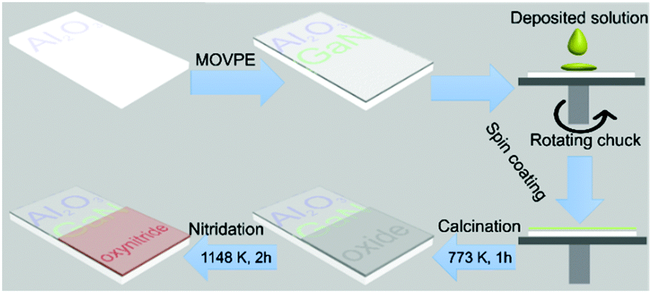 | ||
| Fig. 3 Schematic illustration of the fabrication procedure for semi-transparent quaternary metal oxynitride thin film photoanode on transparent conductive GaN/Al2O3 substrate. | ||
X-ray diffraction (XRD) patterns presented in Fig. 4a reveal that the grown LaTiO2N thin film on Al2O3/GaN substrate is of single-phase purity. The LaTiO2N patterns fully match the simulated powder patterns (ICSD 239555).35 The UV-vis spectrum (Fig. 4b) also shows an absorption edge at approximately 600 nm, consistent with the LaTiO2N band gap of 2.0–2.1 eV.36 The transmittance decreased from 80% on the Al2O3/GaN substrate to roughly 60% on the Al2O3/GaN/LaTiO2N substrate for wavelengths above 600 nm. The high transparency (see inset of Fig. 4b) of LaTiO2N is above the threshold for constructing a tandem PEC cell by integration with a photocathode of smaller band gap. The damping-like feature of the spectrum is due to the interference fringes of multiple layers, i.e. Al2O3, GaN and LaTiO2N.15 The SEM micrograph in Fig. 4c shows the morphology of the prepared LaTiO2N film in the form of a microstructure comprised of nanoparticulate agglomerations that were several hundred nanometers in diameter. A similar morphology is usually obtained for other ceramic thin films prepared by chemical solution deposition (CSD).37 The SEM at low magnification (see Fig. S6, ESI†) demonstrates that the film is uniform and crack-free, the thickness is around 230 nm from the cross-sectional SEM (Fig. S7, ESI†). We also synthesized SrTaO2N in order to verify the generality of the CSD-based synthesis for semi-transparent quaternary oxynitride photoanodes. Its XRD pattern (Fig. 4a) confirms the formation of single phase SrTaO2N crystallizing with the tetragonally-distorted perovskite structure in space group I4/mcm (ICSD 95373).38 The prepared SrTaO2N thin film also exhibited high transparency (see inset of Fig. 4b). UV-vis measurements showed transmittance of approximately 70% for wavelengths above 550 nm, which corresponds to the absorption edge of SrTaO2N.39 The surface of SrTaO2N (SEM, Fig. S8, ESI†) is smoother than for LaTiO2N. However, the thin film thickness is difficult to determine due to strong charging during SEM analysis. These results prove that the CSD-based process can indeed be used for other semi-transparent quaternary oxynitride thin films on transparent Al2O3/GaN substrate.
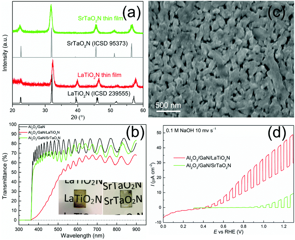 | ||
| Fig. 4 (a) XRD patterns of LaTiO2N and SrTaO2N film on Al2O3/GaN substrate and simulated patterns (ICSD 239555 and 95373). (b) UV-vis transmittance spectra of LaTiO2N and SrTaO2N film on Al2O3/GaN substrate and the substrate before oxynitride formation. The inset depicts a photographic image of the films. (c) SEM micrograph of LaTiO2N film on Al2O3/GaN substrate. (d) LSV curves of LaTiO2N and SrTaO2N films measured in 0.1 M NaOH under chopped AM 1.5G simulated solar light (100 mW cm−2). | ||
The critical feature of such prepared electrodes is the transport of electrons through the GaN pathway over the external circuit to the counter-electrode. The PEC water oxidation performances of the prepared LaTiO2N and SrTaO2N films were assessed in 0.1 M NaOH electrolyte (pH 13) under simulated sunlight (1 sun, AM 1.5G). Fig. 4d displays the LSV curves measured at a scan rate of 10 mV s−1 under chopped illumination. The LaTiO2N thin film developed a net photocurrent of approximately 20 μA cm−2 at 1.23 V vs. RHE. The photocurrent is comparable with the LaTiO2N film deposited on MgO/TiN and Nb:SrTiO3 substrates via PLD and RF sputtering reported by Lippert29 and Domen,26 respectively. The dark-current contribution stems from photocorrosion of the oxynitride surface, which is a common phenomenon for unprotected metal oxynitrides and can be suppressed with protective layers.40,41 The pristine semi-transparent SrTaO2N photoanode, having a slightly larger band gap than LaTiO2N, generated a photocurrent of app. 7 μA cm−2 at 1.23 V vs. RHE. Both LaTiO2N and SrTaO2N films show photoresponse at app. 0 V vs. RHE, indicating relative negative onset potentials (see enlarged view in Fig. S9, ESI†).
In conclusion, we have successfully fabricated semi-transparent quaternary oxynitride LaTiO2N and SrTaO2N thin films on transparent conductive Al2O3/GaN substrate. PEC measurements confirmed their potential for use as the top photoanode in a PEC water-splitting cell, and the band gaps suggest that they may have higher theoretical STH than Ta3N5-based photoanodes. The CSD-based process can be adopted as a general method towards the manufacture of semi-transparent quaternary oxynitride thin films on large scale. Additionally, the conductive Al2O3/GaN substrate have been coated with TaOxNy by means of ALD to yield semi-transparent thin films. Nonetheless, the photocurrent of the quaternary oxynitride thin film is far lower in comparison to their maximum theoretical values. This requires future synthetic strategies for nanostructuring below 100 nm of the light absorbing metal oxynitride layer and its subsequent semi-transparent catalysts.
A. S. thanks Vinnova (project: C1Bio 2019-03174) for financial support. R. H. C. and J. R. D. are supported by the U.S. DOE, Office of Science, Office of Basic Energy Sciences (no. DE-SC-0020301). Z. M. thanks the China Scholarship Council for a PhD scholarship. We thank Wenyan Wang for the access to UV-vis facilities. XPS measurements were done with equipment purchased with the financial support of the EU Regional Development Fund (no. POIG.02.01.00-12-023/08).
Conflicts of interest
There are no conflicts to declare.Notes and references
- S. A. Monny, Z. Wang, T. Lin, P. Chen, B. Luo and L. Wang, Chem. Commun., 2020, 56, 9376–9379 RSC.
- J. H. Kim, H. Kaneko, T. Minegishi, J. Kubota, K. Domen and J. S. Lee, ChemSusChem, 2016, 9, 61–66 CrossRef CAS.
- Q. Zeng, J. Bai, J. Li, B. Zhou and Y. Sun, Nano Energy, 2017, 41, 225–232 CrossRef CAS.
- M. S. Prévot and K. Sivula, J. Phys. Chem. C, 2013, 117, 17879–17893 CrossRef.
- K. Walczak, Y. Chen, C. Karp, J. W. Beeman, M. Shaner, J. Spurgeon, I. D. Sharp, X. Amashukeli, W. West, J. Jin, N. S. Lewis and C. Xiang, ChemSusChem, 2015, 8, 544–551 CrossRef CAS.
- T. Sekimoto, H. Hashiba, S. Shinagawa, Y. Uetake, M. Deguchi, S. Yotsuhashi and K. Ohkawa, Jpn. J. Appl. Phys., 2016, 55, 088004 CrossRef.
- Y. Chen, X. Feng, Y. Liu, X. Guan, C. Burda and L. Guo, ACS Energy Lett., 2020, 5, 844–866 CrossRef CAS.
- K. Zhang, M. Ma, P. Li, D. H. Wang and J. H. Park, Adv. Energy Mater., 2016, 6, 1600602 CrossRef.
- Y. Fang, D. Commandeur, W. C. Lee and Q. Chen, Nanoscale Adv., 2020, 2, 626–632 RSC.
- H. Hajibabaei, O. Zandi and T. W. Hamann, Chem. Sci., 2016, 7, 6760–6767 RSC.
- K. Sivula and R. van de Krol, Nat. Rev. Mater., 2016, 1, 15010 CrossRef CAS.
- R. J. Detz, J. N. H. Reek and B. C. C. van der Zwaan, Energy Environ. Sci., 2018, 11, 1653–1669 RSC.
- C. R. Lhermitte, A. Polo, L. Yao, F. A. Boudoire, N. Guijarro and K. Sivula, ChemSusChem, 2020, 13, 3645–3653 CrossRef CAS.
- H. Hajibabaei, D. J. Little, A. Pandey, D. Wang, Z. Mi and T. W. Hamann, ACS Appl. Mater. Interfaces, 2019, 11, 15457–15466 CrossRef CAS.
- T. Higashi, H. Nishiyama, Y. Suzuki, Y. Sasaki, T. Hisatomi, M. Katayama, T. Minegishi, K. Seki, T. Yamada and K. Domen, Angew. Chem., Int. Ed., 2019, 58, 2300–2304 CrossRef CAS.
- T. Higashi, H. Nishiyama, Y. Otsuka, Y. Kawase, Y. Sasaki, M. Nakabayashi, M. Katayama, T. Minegishi, N. Shibata, K. Takanabe, T. Yamada and K. Domen, ChemSusChem, 2020, 13, 1974–1978 CrossRef CAS.
- D. Akagi, Y. Kageshima, Y. Hashizume, S. Aoi, Y. Sasaki, H. Kaneko, T. Higashi, T. Hisatomi, M. Katayama, T. Minegishi, S. Noda and K. Domen, ChemPhotoChem, 2019, 3, 521–524 CrossRef CAS.
- J. Seo, T. Takata, M. Nakabayashi, T. Hisatomi, N. Shibata, T. Minegishi and K. Domen, J. Am. Chem. Soc., 2015, 137, 12780–12783 CrossRef CAS.
- Y. He, J. E. Thorne, C. H. Wu, P. Ma, C. Du, Q. Dong, J. Guo and D. Wang, Chem, 2016, 1, 640–655 CAS.
- C. Xiang, A. Z. Weber, S. Ardo, A. Berger, Y. Chen, R. Coridan, K. T. Fountaine, S. Haussener, S. Hu, R. Liu, N. S. Lewis, M. A. Modestino, M. M. Shaner, M. R. Singh, J. C. Stevens, K. Sun and K. Walczak, Angew. Chem., Int. Ed., 2016, 55, 12974–12988 CrossRef CAS.
- Z. Ma, A. Jaworski, J. George, A. Rokicinska, T. Thersleff, T. M. Budnyak, G. Hautier, A. J. Pell, R. Dronskowski, P. Kuśtrowski and A. Slabon, J. Phys. Chem. C, 2020, 124, 152–160 CrossRef CAS.
- J. Seo, H. Nishiyama, T. Yamada and K. Domen, Angew. Chem., Int. Ed., 2018, 57, 8396–8415 CrossRef CAS.
- A. P. Black, H. Suzuki, M. Higashi, C. Frontera, C. Ritter, C. De, A. Sundaresan, R. Abe and A. Fuertes, Chem. Commun., 2018, 54, 1525–1528 RSC.
- A. Fuertes, Mater. Horizons, 2015, 2, 453–461 RSC.
- T. Wakasugi, Y. Hirose, S. Nakao, Y. Sugisawa, D. Sekiba and T. Hasegawa, ACS Omega, 2020, 5, 13396–13402 CrossRef CAS.
- C. Le Paven-Thivet, A. Ishikawa, A. Ziani, L. Le Gendre, M. Yoshida, J. Kubota, F. Tessier and K. Domen, J. Phys. Chem. C, 2009, 113, 6156–6162 CrossRef CAS.
- C. Le Paven, A. Ziani, F. Marlec, L. Le Gendre, F. Tessier, M. Haydoura, R. Benzerga, F. Cheviré, K. Takanabe and A. Sharaiha, J. Eur. Ceram. Soc., 2020, 1–8 Search PubMed.
- C. Le Paven-Thivet, L. Le Gendre, J. Le Castrec, F. Cheviré, F. Tessier and J. Pinel, Prog. Solid State Chem., 2007, 35, 299–308 CrossRef CAS.
- C. Lawley, M. Nachtegaal, J. Stahn, V. Roddatis, M. Döbeli, T. J. Schmidt, D. Pergolesi and T. Lippert, Nat. Commun., 2020, 11, 1728 CrossRef CAS.
- F. Haydous, M. Döbeli, W. Si, F. Waag, F. Li, E. Pomjakushina, A. Wokaun, B. Gökce, D. Pergolesi and T. Lippert, ACS Appl. Energy Mater., 2019, 2, 754–763 CrossRef CAS.
- Y. Pihosh, V. Nandal, T. Minegishi, M. Katayama, T. Yamada, K. Seki, M. Sugiyama and K. Domen, ACS Energy Lett., 2020, 5, 2492–2497 CrossRef CAS.
- P. J. Reed, H. Mehrabi, Z. G. Schichtl and R. H. Coridan, ACS Appl. Mater. Interfaces, 2018, 10, 43691–43698 CrossRef CAS.
- H.-D. Xiao, H.-L. Ma, C.-S. Xue, H.-Z. Zhuang, J. Ma, F.-J. Zong and W.-R. Hu, Mater. Lett., 2005, 59, 4041–4043 CrossRef CAS.
- B. A. Pinaud, A. Vailionis and T. F. Jaramillo, Chem. Mater., 2014, 26, 1576–1582 CrossRef CAS.
- D. Habu, Y. Masubuchi, S. Torii, T. Kamiyama and S. Kikkawa, J. Solid State Chem., 2016, 237, 254–257 CrossRef CAS.
- K. Kawashima, M. Hojamberdiev, H. Wagata, K. Yubuta, J. J. M. Vequizo, A. Yamakata, S. Oishi, K. Domen and K. Teshima, J. Phys. Chem. C, 2015, 119, 15896–15904 CrossRef CAS.
- A. V. Prasadarao, U. Selvaraj and S. Komarnenici, J. Mater. Res., 1995, 10, 704–707 CrossRef CAS.
- S. J. Clarke, K. A. Hardstone, C. W. Michie and M. J. Rosseinsky, Chem. Mater., 2002, 14, 2664–2669 CrossRef CAS.
- A. Iborra-Torres, A. N. Kulak, R. G. Palgrave and G. Hyett, ACS Appl. Mater. Interfaces, 2020, 12, 33603–33612 CrossRef CAS.
- C. M. Leroy, A. E. Maegli, K. Sivula, T. Hisatomi, N. Xanthopoulos, E. H. Otal, S. Yoon, A. Weidenkaff, R. Sanjines and M. Grätzel, Chem. Commun., 2012, 48, 820–822 RSC.
- Z. Ma, T. Thersleff, A. L. Görne, N. Cordes, Y. Liu, S. Jakobi, A. Rokicinska, Z. G. Schichtl, R. H. Coridan, P. Kustrowski, W. Schnick, R. Dronskowski and A. Slabon, ACS Appl. Mater. Interfaces, 2019, 11, 19077–19086 CrossRef CAS.
Footnote |
| † Electronic supplementary information (ESI) available. See DOI: 10.1039/d0cc04894a |
| This journal is © The Royal Society of Chemistry 2020 |