
Reconstructed transparent conductive layers of fluorine doped tin oxide for greatly weakened hysteresis and improved efficiency of perovskite solar cells†
Jinbo
Wu‡
ab,
Chao
Zhen‡
a,
Tingting
Wu
ab,
Chunxu
Jia
ab,
Mustafa
Haider
ac,
Gang
Liu
 *ab and
Hui-Ming
Cheng
ad
*ab and
Hui-Ming
Cheng
ad
aShenyang National Laboratory for Materials Science, Institute of Metal Research, Chinese Academy of Sciences, 72 Wenhua Road, Shenyang 110016, China. E-mail: gangliu@imr.ac.cn
bSchool of Materials Science and Engineering, University of Science and Technology of China, 72 Wenhua Road, Shenyang 110016, China
cUniversity of Chinese Academy of Sciences, 19(A) Yuquan Road, Beijing, 100049, China
dLow-Dimensional Material and Device Laboratory, Tsinghua-Berkeley Shenzhen Institute, Tsinghua University, 1001 Xueyuan Road, Shenzhen 518055, China
First published on 4th December 2019
Abstract
Reconstructed transparent conductive films of fluorine doped tin oxide on glass substrates synthesized by electrochemical reduction followed by thermal oxidation were demonstrated to be effective in collecting photogenerated electrons in planar perovskite solar cells. Compared to the cells fabricated with the pristine film, the cell based on the reconstructed film shows an improved power conversion efficiency under forward scan from 9% to 15.1% and greatly weakened hysteresis behavior.
Metal halide perovskites have emerged as a promising candidate of photovoltaic materials due to the low cost, simple fabrication and charming optoelectronic properties possessed in this family of materials, such as large light-absorption coefficients, high carrier mobilities and long carrier diffusion lengths.1–5 These unique intrinsic properties enable the perovskite active layer thickness of around 500 nm in perovskite solar cells (PSCs) to be smaller than the photocarrier effective diffusion lengths (>1 μm), suggesting that photogenerated carriers can effectively reach the interfaces contacting with electron- and hole-selective layers (ESL and HSL) before recombinations.3,6 Consequently, the ESL and HSL themselves are crucial in determining the device performance, and they are required to have high efficiencies in selectively collecting photoelectrons and photoholes, respectively.7,8
Highly efficient PSCs have been frequently achieved by using TiO2 as the ESL component9,10 However, the device stability has been remarkably abated by the trapped charges and the photocatalytic effect of TiO2.11 SnO2 as the ESL component in planar PSCs has attracted much attention in the past few years due to its high electron mobility, low density of surface defects, appropriate band edge alignments and weak photocatalytic activity.12,13 Although efficient planar PSCs based on the SnO2 ESLs have been achieved,14–17 an extra SnO2 precursor is always needed to prepare SnO2 ESLs, increasing process complexity and fabrication costs.
Since the achieved PCE of PSCs has met the commercial requirement to date, increasing effort has been focused on the operational area and long-term durability of cells to promote the commercialization.18–20 Simplifying the PSC structure by reducing the use of HSL, ESL and metal electrodes is an alternative approach to accelerate the commercialization process.21,22 Although the ESL-free PSCs show efficiencies comparable with the regular structure devices,22–25 they show a much stronger hysteresis behavior than the regular structure ones.
Inspired by the fact that the matrix material of the most typical transparent conductive oxide (TCO) layers supported on glass substrates as the bottom electrodes of regular PSCs is doped SnO2 (i.e., FTO, fluorine doped SnO2),11,26 we propose to produce an integrated substrate of SnO2-FTO for building efficient and weak hysteresis planar PSCs. Compared to other transition metal oxides like TiO2, one remarkable feature of SnO2 is the easy loss of anion atoms when exposed to reductive conditions. Since FTO is prepared by introducing F elements into the oxygen lattices of SnO2 crystals, SnO2 might be obtained by removing F dopants from FTO. To conformally form an ultrathin SnO2 layer on the surface of FTO, we present an electrochemical reduction process to rationally remove F from the surface of the FTO layer, followed by a thermal oxidation process to recover F vacancy related defects by oxygen atoms (Fig. 1). Finally, we obtained the FTO substrate covered with an ultrathin SnO2 top-layer. The device based on the pristine FTO substrate delivers an efficiency of ∼14% under reverse scan, similar to the previous literature report,22,23 but it shows a strong hysteresis loop and its efficiency under forward scan is only 9%. In contrast, the device with the modified FTO substrate (O-R-FTO) can give an improved efficiency of 15.7% and it shows a much weak hysteresis behavior with a forward scan efficiency of 15.1%.
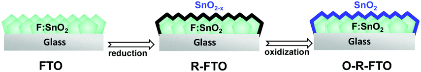 | ||
| Fig. 1 Schematic of the formation of an ultrathin SnO2 layer on the FTO substrate surface. | ||
The electrochemical process proceeding at the solid/electrolyte interface provides an effective strategy to selectively remove F element from the FTO surface. Metal oxides are easily reduced to metal sub-oxides via an electrochemical reduction process.27,28 Here, FTO was electrochemically reduced in a three-electrode system, in which a Pt foil was used as the counter electrode, a saturated calomel electrode (SCE) as the reference electrode, and Na2SO3 aqueous solution (1 M) as the electrolyte. The cyclic voltammetry curve was recorded to analyze the possible surface reactions of FTO at different potentials (Fig. 2a). A reductive peak of −1.56 V appearing at the initial phase of the hydrogen evolution reaction (HER) corresponds to the reduction process from SnO2 to SnO2−x. Further reduction at a more negative bias leads to a sharp current increase, accompanying the colour change of FTO from transparent to black. This phenomenon can be explained as a result of the strong HER process and a further reduction of SnO2 into Sn. Two oxidation peaks at −1.3 V and −0.6 V appearing in the following reverse anode scan correspond to the re-oxidation of the newly formed Sn back to SnO and SnO2, respectively.
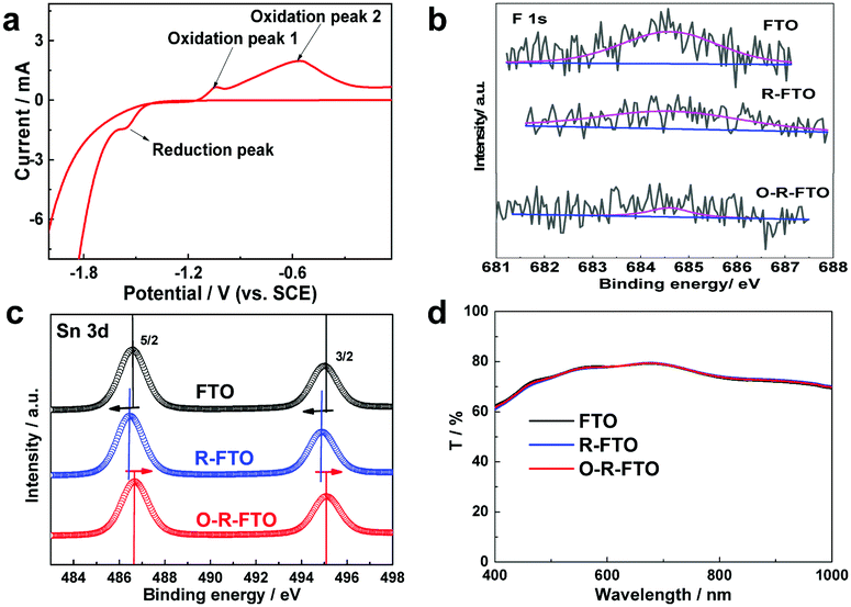 | ||
| Fig. 2 (a) The cyclic voltammetry curves recorded on the FTO substrate in the three electrode electrochemical system; XPS (b) F 1s and (c) Sn 3d spectra of the pristine FTO, R-FTO and O-R-FTO surfaces. (d) Transmittance spectra of the pristine FTO, R-FTO and O-R-FTO supported on glass substrates. | ||
On the basis of the above results, the potential of −1.56 V (vs. SCE) was applied to electrochemically reduce FTO in order to remove surface F dopants from FTO. Generally, metal-halide bonds are more easily broken down during the electrochemical reduction process as compared to metal–oxygen bonds due to their stronger ionic bonding character. So, it was proposed that surface FTO (F:SnO2) can be reduced to SnO2−x under mild reduction conditions, and the following thermal oxidation of SnO2−x in air can lead to the formation of SnO2 by healing anionic vacancy defects. To verify this proposal, FTO was reduced electrochemically at −1.56 V for 150 s, and then heated at 470 °C for 60 min. Heating at above 450 °C for over 30 min is always necessary to improve the crystallinity of the newly formed SnO2 top layer and also the quality of its interface with the FTO mother substrate. Comparison of X-ray diffraction (XRD) patterns and scanning electron microscopy (SEM) images of the pristine FTO, electrochemically reduced FTO (R-FTO) and re-oxidized R-FTO (O-R-FTO) (Fig. S1 and S2, ESI†) suggests the well retained crystal structures and surface morphologies of the FTO layer after the electrochemical reduction and thermal oxidation. Surface components of three FTO layers were investigated by X-ray photoelectron spectroscopy (XPS). The greatly weakened XPS F 1s signal after the electrochemical reduction (Fig. 2b) suggests the heavy loss of fluorine from the FTO surface as anticipated. Further oxidation leads to the full removal of surface fluorine. Meanwhile, the binding energy of Sn 3d3/2 and Sn 3d5/2 shifts towards lower energy (Fig. 2c), which means that the valence state of Sn ions is reduced as a result of the formation of anionic vacancies. After heating treatment, the F 1s signal is further weakened to be negligible for O-R-FTO due to the evaporation of F species. The binding energy of Sn 3d3/2 and Sn 3d5/2 shifts back to high energy because of the removal of the anionic vacancies during the thermal treatment. Transmittance is an important parameter of TCO substrates for building efficient PSCs. The FTO, R-FTO and O-R-FTO show similar transmittance in the whole visible light range (Fig. 2d).
Perovskite films were spin-coated on the FTO and O-R-FTO substrates using identical procedures, and the details have been described in the supplementary information. The XRD patterns of perovskite layers deposited on the FTO and O-R-FTO substrates are nearly the same (Fig. 3a), indicating the formation of the perovskite crystal structure with similar crystallinity and grain sizes. The perovskite films have very similar absorption spectra that show a band gap of 1.56 eV (Fig. 3b).29 SEM images (Fig. 3c, d and Fig. S3, ESI†) show a similar morphology of smooth and dense films with the crystal grain size of hundreds of nanometers on three different FTO substrates. All these results consistently demonstrate the formation of very similar perovskite films with comparable properties on the FTO and O-R-FTO substrates.
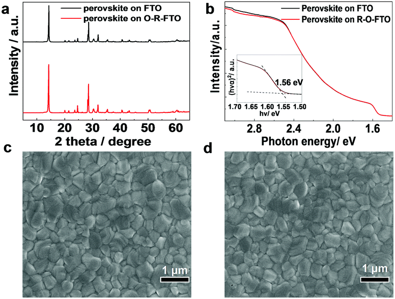 | ||
| Fig. 3 (a) XRD patterns and (b) absorption spectra of perovskite films coated on the FTO and O-R-FTO substrates; (c and d) SEM images of the perovskite films on the FTO and O-R-FTO substrates, respectively. | ||
Perovskite solar cells were assembled by sequentially spin-coating Spiro-OMeTAD HSL and thermal-evaporating an Au counter electrode on the perovskite films coated on the FTO and O-R-FTO substrates with the architecture of FTO (or O-R-FTO)/perovskite/Spiro-OMeTAD/Au. Electrochemical reduction duration is a crucial parameter of modifying the FTO substrate.
The ideal case is forming a uniform thin layer of SnO2−x that can be transformed into SnO2 in the following thermal treatment. The short reduction duration may result in the partial exposure of the pristine FTO surface, which increases the photo-carrier recombination paths at the FTO/perovskite film interface. The long reduction duration may result in a thick SnO2 layer at the FTO surface, which causes an increase in the series resistance of the devices. To find the optimal electrochemical reduction duration, perovskite solar cells were fabricated based on O-R-FTO substrates with different durations of the electrochemical reduction at −1.56 V (Fig. 4a and Fig. S4, ESI†). Solar cells fabricated with O-R-FTO substrates with screened reduction durations of 120 s, 150 s and 180 s show champion efficiencies of 15.3%, 15.7% and 14.7%, respectively (Fig. 4a). The electrochemical reduction duration used in this study is therefore 150 s. Due to the same crystal structure and overlapping compositions of Sn and O between the SnO2 layer and the FTO mother substrate, their interface cannot be recognized from the cross-section SEM images (Fig. S5, ESI†). To evaluate the thickness of the newly formed SnO2 layer, the depth dependent XPS spectra of F 1s upon Ar+ sputtering (1 Å s−1) were recorded. The intensity of the F species signal was negligible before the 30 s sputtering. The signal is obvious after the 50 s sputtering (Fig. S6, ESI†), indicating a thickness of 3–5 nm SnO2 top layer. To clarify the superiority of O-R-FTO as the TCO substrate for building PSCs, the devices respectively based on FTO and O-R-FTO substrates were assembled and tested under solar simulator illumination with a power density of 95 mW cm−2. Fig. 4b compares the J–V curves of the solar cells with the FTO and O-R-FTO substrates. Although the cell with the FTO substrate delivers an efficiency of around 14% under reverse scan (similar to the previous literature report),22,23 it shows a strong hysteresis loop and its efficiency under forward scan is only 9.0%. In contrast, the cell with an O-R-FTO substrate exhibits an efficiency of 15.7% and shows a much weaker hysteresis behavior with a forward scan efficiency of 15.1%. Photovoltaic parameters of the cells with the FTO and O-R-FTO substrates are listed in Table S1 (ESI†). The PSC of the FTO substrate based cell shows a short current density (Jsc) of 18.82 mA cm−2, open-circuit voltage (Voc) of 0.97 V, and fill factor (FF) of 0.73 under reverse scan. The PSC of the O-R-FTO substrate based cell exhibits a Jsc of 21.13 mA cm−2, Voc of 1.04 V, and FF of 0.675 under reverse scan. To statistically validate the performance enhancement enabled by the FTO modification, tens of cells with the FTO and O-R-FTO substrates were compared. The cells with the O-R-FTO substrates give an average efficiency of 14.3% and a champion efficiency of 15.7%, which are higher than the average efficiency (13.1%) and the champion efficiency (14%) yielded by the cells with the FTO substrates (Fig. 4c). The incident photon-to-electron conversion efficiency (IPCE) measurement was carried out on the champion cells (Fig. 4d). The IPCE values of the cell with the O-R-FTO substrate are around 10% higher than that of the cell with the FTO substrate in the whole visible light range. The integrated photocurrent densities calculated from the IPCE spectra are 21.05 mA cm−2 for the O-R-FTO based cell and 18.88 mA cm−2 for the FTO based cell according to the standard solar spectrum, which are in accordance with current density values recorded from J–V curves. Additionally, the O-R-FTO based cell shows better stability at maximum power point than the FTO based cell (Fig. S7, ESI†).
 | ||
| Fig. 4 (a) J–V curves of PSCs based on O-R-FTO substrates with different electrochemical reduction durations (120 s, 150 s and 180 s) at −1.56 V; (b) J–V curves of the champion devices based on the FTO and O-R-FTO substrates; (c) PCE distribution histogram, (d) IPCE spectra and their corresponding integrated current density curves of PSCs on the FTO and O-R-FTO substrates. | ||
To elucidate the performance improvement mechanism, the electron extracting ability of the FTO and O-R-FTO substrates was evaluated by using photoluminescence (PL) spectroscopy. Steady state PL spectra recorded on the perovskite films coated on glass, FTO and O-R-FTO substrates were compared in Fig. 5a. Perovskite films on these three substrates show a similar PL peak position at 1.56 eV, corresponding to the band-to-band radiative recombination in perovskite. The highest PL intensity of the perovskite film supported on the glass substrate case is attributed to the confinement of the photo-carriers. The PL is greatly quenched for the films supported on the FTO and O-R-FTO cases, which means that the photo-electrons can be effectively collected by the FTO and O-R-FTO substrates as ESL. Since the Fermi levels of both FTO and the conduction band minimum (CBM) of SnO2 are located below the CBM of the perovskite, the photo-electrons generated in the perovskite films can effectively transfer to FTO and O-R-FTO.15,23,29 Although the photo-electrons can effectively transfer to FTO (Fig. S8, ESI†), the photo-holes in the perovskite film can also transfer to FTO, resulting in the recombination at the perovskite/FTO interface. This interface recombination causes the decrease of Jsc and Voc. It is noteworthy that the PL quenching efficiency is the highest for the O-R-FTO case. The reason is that the O-R-FTO surface covered by an extremely thin SnO2 film can effectively extract electrons and block holes simultaneously.15 This suggests that the O-R-FTO film can act as a better TCO substrate than pristine FTO in PSCs. These steady state PL results are in accordance with the performance improvement characteristics of the cells. The time-resolved PL spectra recorded from the perovskite films on the pristine FTO and O-R-FTO substrates (Fig. 5b) further support this conclusion. A bi-exponent decay model is generally adopted to analyze photo-carrier dynamics in perovskite films contacting with ESLs (or HSLs) as shown in Table S2 (ESI).†![[thin space (1/6-em)]](https://www.rsc.org/images/entities/char_2009.gif) 30,31 The short decay time τ1 corresponds to the transfer process across interfaces, while the long decay time τ2 is related to the bulk recombination process in the perovskite. The stimulation results give τ1, 1.86 ns and τ2, 93.71 ns for the O-R-FTO substrate case, which are smaller than that (τ1, 1.92 ns and τ2, 136.25 ns) for the FTO case. This suggests that the O-R-FTO substrate can extract electrons more efficiently than the pristine FTO substrate.
30,31 The short decay time τ1 corresponds to the transfer process across interfaces, while the long decay time τ2 is related to the bulk recombination process in the perovskite. The stimulation results give τ1, 1.86 ns and τ2, 93.71 ns for the O-R-FTO substrate case, which are smaller than that (τ1, 1.92 ns and τ2, 136.25 ns) for the FTO case. This suggests that the O-R-FTO substrate can extract electrons more efficiently than the pristine FTO substrate.
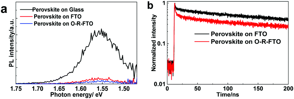 | ||
| Fig. 5 (a) Steady state photoluminescence spectra of three perovskite films supported on the glass, pristine FTO and O-R-FTO substrates; (b) time resolved photoluminescence spectra of the perovskite films supported on the pristine FTO and O-R-FTO substrates. | ||
In summary, transparent conductive films of FTO supported on glass substrates were reconstructed by electrochemical reduction, followed by thermal oxidation in air. Compared to the pristine FTO film, the surface layer of the reconstructed O-R-FTO films consists of fluorine-free SnO2. PSCs built with the O-R-FTO substrates deliver a champion efficiency of 15.7% under reverse scan and 15.1% under forward scan, giving a negligible hysteresis behavior. In contrast, PSCs based on the pristine FTO substrates show a champion efficiency of 14.0% under reverse scan and 9.0% under forward scan, giving a strong hysteresis. The superior performance of the cells based on the O-R-FTO substrates was attributed to the increased ability of selectively collecting photo-electrons by the O-R-FTO with an ultrathin SnO2 layer. The developed strategies of modifying traditional FTO substrates to increase the ability of collecting photo-electrons may provide an alternative route to further simplify the device fabrication procedures and reduce its production costs.
The authors thank the National Natural Science Foundation of China (No. 51825204), and the Key Research Program of Frontier Sciences CAS (QYZDB-SSW-JSC039) for the financial support.
Conflicts of interest
There are no conflicts to declare.Notes and references
- A. Abate, J.-P. Correa-Baena, M. Saliba, M. S. Su'ait and F. Bella, Chem. – Eur. J., 2018, 24, 3083–3100 CrossRef CAS PubMed.
- W. J. Yin, T. Shi and Y. Yan, Adv. Mater., 2014, 26, 4653–4658 CrossRef CAS.
- D. Shi, V. Adinolfi, R. Comin, M. Yuan, E. Alarousu, A. Buin, Y. Chen, S. Hoogland, A. Rothenberger, K. Katsiev, Y. Losovyj, X. Zhang, P. A. Dowben, O. F. Mohammed, E. H. Sargent and O. M. Bakr, Science, 2015, 347, 519–522 CrossRef CAS.
- S. D. Stranks, G. E. Eperon, G. Grancini, C. Menelaou, M. J. P. Alcocer, T. Leijtens, L. M. Herz, A. Petrozza and H. J. Snaith, Science, 2013, 342, 341–344 CrossRef CAS.
- G. Xing, N. Mathews, S. Sun, S. S. Lim, Y. M. Lam, M. Grätzel, S. Mhaisalkar and T. C. Sum, Science, 2013, 342, 344–347 CrossRef CAS.
- M. M. Lee, J. Teuscher, T. Miyasaka, T. N. Murakami and H. J. Snaith, Science, 2012, 338, 643–647 CrossRef CAS.
- G. Yang, H. Tao, P. Qin, W. Ke and G. Fang, J. Mater. Chem. A, 2016, 4, 3970–3990 RSC.
- L. Calio, S. Kazim, M. Grätzel and S. Ahmad, Angew. Chem., Int. Ed., 2016, 55, 14522–14545 CrossRef CAS.
- H. Zhou, Q. Chen, G. Li, S. Luo, T.-B. Song, H.-S. Duan, Z. Hong, J. You, Y. Liu and Y. Yang, Science, 2014, 345, 542–546 CrossRef CAS.
- H. Tan, A. Jain, O. Voznyy, X. Lan, F. P. G. de Arquer, J. Z. Fan, R. Quintero-Bermudez, M. Yuan, B. Zhang, Y. Zhao, F. Fan, P. Li, L. N. Quan, Y. Zhao, Z.-H. Lu, Z. Yang, S. Hoogland and E. H. Sargent, Science, 2017, 355, 722–726 CrossRef CAS.
- T. Leijtens, G. E. Eperon, S. Pathak, A. Abate, M. M. Lee and H. J. Snaith, Nat. Commun., 2013, 4, 2885 CrossRef.
- A. J. Nozik and R. Memming, J. Phys. Chem., 1996, 100, 13061–13078 CrossRef CAS.
- Q. Jiang, X. Zhang and J. You, Small, 2018, 14, 1801154 CrossRef.
- J. P. Correa Baena, L. Steier, W. Tress, M. Saliba, S. Neutzner, T. Matsui, F. Giordano, T. J. Jacobsson, A. R. Srimath Kandada, S. M. Zakeeruddin, A. Petrozza, A. Abate, M. K. Nazeeruddin, M. Grätzel and A. Hagfeldt, Energy Environ. Sci., 2015, 8, 2928–2934 RSC.
- Q. Jiang, L. Zhang, H. Wang, X. Yang, J. Meng, H. Liu, Z. Yin, J. Wu, X. Zhang and J. You, Nat. Energy, 2016, 2, 16177 CrossRef.
- T. T. Wu, C. Zhen, J. B. Wu, C. X. Jia, M. Haider, L. Z. Wang, G. Liu and H. M. Cheng, Sci. Bull., 2019, 64, 547–552 CrossRef CAS.
- E. H. Anaraki, A. Kermanpur, L. Steier, K. Domanski, T. Matsui, W. Tress, M. Saliba, A. Abate, M. Grätzel, A. Hagfeldt and J.-P. Correa-Baena, Energy Environ. Sci., 2016, 9, 3128–3134 RSC.
- F. Huang, M. Li, P. Siffalovic, G. Cao and J. Tian, Energy Environ. Sci., 2019, 12, 518–549 RSC.
- Q. Hu, H. Wu, J. Sun, D. Yan, Y. Gao and J. Yang, Nanoscale, 2016, 8, 5350–5357 RSC.
- H. Back, G. Kim, J. Kim, J. Kong, T. K. Kim, H. Kang, H. Kim, J. Lee, S. Lee and K. Lee, Energy Environ. Sci., 2016, 9, 1258–1263 RSC.
- A. Mei, X. Li, L. Liu, Z. Ku, T. Liu, Y. Rong, M. Xu, M. Hu, J. Chen, Y. Yang, M. Grätzel and H. Han, Science, 2014, 345, 295–298 CrossRef CAS.
- D. Liu, J. Yang and T. L. Kelly, J. Am. Chem. Soc., 2014, 136, 17116–17122 CrossRef CAS.
- W. Ke, G. Fang, J. Wan, H. Tao, Q. Liu, L. Xiong, P. Qin, J. Wang, H. Lei, G. Yang, M. Qin, X. Zhao and Y. Yan, Nat. Commun., 2015, 6, 6700 CrossRef CAS.
- H. Yu, J. Ryu, J. W. Lee, J. Roh, K. Lee, J. Yun, J. Lee, Y. K. Kim, D. Hwang, J. Kang, S. K. Kim and J. Jang, ACS Appl. Mater. Interfaces, 2017, 9, 8113–8120 CrossRef CAS.
- H. Yu, J. W. Lee, J. Yun, K. Lee, J. Ryu, J. Lee, D. Hwang, S. K. Kim and J. Jang, Adv. Energy Mater., 2017, 7, 1700749 CrossRef.
- X. Dong, X. Fang, M. Lv, B. Lin, S. Zhang, J. Ding and N. Yuan, J. Mater. Chem. A, 2015, 3, 5360–5367 RSC.
- Z. Peng, S. A. Freunberger, Y. Chen and P. G. Bruce, Science, 2012, 337, 563–566 CrossRef CAS.
- J. M. Macak, C. Zollfrank, B. J. Rodriguez, H. Tsuchiya, M. Alexe, P. Creil and P. Schmuki, Adv. Mater., 2009, 21, 3121–3125 CrossRef CAS.
- V. Tallapally, T. A. Nakagawara, D. O. Demchenko, U. Ozguer and I. U. Arachchige, Nanoscale, 2018, 10, 20296–20305 RSC.
- M. Haider, C. Zhen, T. T. Wu, J. B. Wu, C. X. Jia, G. Liu and H. M. Cheng, Chem. Commun., 2019, 55, 5343–5346 RSC.
- M. Haider, C. Zhen, T. T. Wu, G. Liu and H. M. Cheng, J. Mater. Sci. Technol., 2018, 34, 1474–1480 CrossRef.
Footnotes |
| † Electronic supplementary information (ESI) available. See DOI: 10.1039/c9cc08102j |
| ‡ The two authors contributed equally. |
| This journal is © The Royal Society of Chemistry 2020 |