
 Open Access Article
 This Open Access Article is licensed under a Creative Commons Attribution-Non Commercial 3.0 Unported Licence
Are plasmonic optical biosensors ready for use in point-of-need applications?
Juanjuan
Liu
,
Mahsa
Jalali
,
Sara
Mahshid
and
Sebastian
Wachsmann-Hogiu
 *
*
Department of Bioengineering, McGill University, Montreal, Quebec, Canada. E-mail: Sebastian.wachsmannhogiu@mcgill.ca
First published on 12th December 2019
Abstract
Plasmonics has drawn significant attention in the area of biosensors for decades due to the unique optical properties of plasmonic resonant nanostructures. While the sensitivity and specificity of molecular detection relies significantly on the resonance conditions, significant attention has been dedicated to the design, fabrication, and optimization of plasmonic substrates. The adequate choice of materials, structures, and functionality goes hand in hand with a fundamental understanding of plasmonics to enable the development of practical biosensors that can be deployed in real life situations. Here we provide a brief review of plasmonic biosensors detailing most recent developments and applications. Besides metals, novel plasmonic materials such as graphene are highlighted. Sensors based on Surface Plasmon Resonance (SPR), Localized Surface Plasmon Resonance (LSPR), and Surface Enhanced Raman Spectroscopy (SERS) are presented and classified based on their materials and structure. In addition, most recent applications to environment monitoring, health diagnosis, and food safety are presented. Potential problems related to the implementation in such applications are discussed and an outlook is presented.
1. Introduction
Biosensors show great potential in many areas such as medical diagnosis, food safety, and environmental monitoring.1–3 When it comes to the detection of analytes such as disease biomarkers or contaminants, it is important to develop accurate biosensors that have high sensitivity and specificity. In general, biosensors utilize a bioreceptor as recognition element (a molecule capable of specifically binding to the analyte) and a transducer (an interface such as electrodes or nanoparticles) to convert analyte binding events into a readable signal. Analytical biosensors can provide accurate concentrations of the analyte due their linear relationship between the concentration and intensity of the detected signal. As a result, by means of a figure of merit, they provide an intuitive way to compare the sensitivity between different biosensors.4 Based on the detected signal, biosensors can be classified as optical (such as plasmonic biosensors), electrochemical, piezoelectric, or magnetic biosensors.5 Among these biosensors, optical biosensors are one of the most commonly used techniques for analytical biosensing due to their high sensitivity and specificity, potential for multiplexing, low noise background, and small volume sample.4There are several review articles discussing the plasmonic biosensors which emphasize on different aspects of this field including the materials, fabrication method, and functionalization. For example, J. R. Mejía-Salazar et al. reviews the advances in plasmonic biosensing using new materials with unique properties focused on the manufacturing of portable devices.6 Longhua Tang et al., on the other hand, specifically reviews the advances colorimetric biosensors for molecular diagnosis.7 Other aspects such as chemical functionalization,8 and operating principles9 of plasmonics-based biosensors have also been reviewed in recent years. More recently, review articles on the topics of comprehensive understanding and discussion on expectations for the near future development of SERS,10 plasmonic biosensors for point-of-care diagnosis applications,11 and carbon-based materials for SPR biosensors,12 were published. Here, we highlighted the potential of plasmonic biosensors in point-of-need applications with respect to the following aspects: (a) the fundamental principles and mechanisms that allow development of plasmonic biosensors, with emphasis on metallic structures and graphene (b) the materials and structures used to transduce the analyte binding events into an optical signal, (c) the applications to real life situations, and (d) their future potential and limitations.
2. Fundamentals of plasmonic materials
Plasmonics studies the interaction of light with metals or metallic nanostructures. Other materials such as graphene also exhibit plasmonic resonance due to the availability of conductive electrons. Plasmonics combines techniques from photonics and electronics at the nanoscale to perform optical measurements of spectra and refractive index changes (via reflection angles) that are related to the chemical structure, or binding events, and can help extract valuable information about the presence, concentration, or identity of molecules of interest.13,14 The study of plasmonics relies on localized or propagating surface plasmons (SPs), which are collective (coherent) oscillations of electrons in the metal, and are generated by the coupling of the incident oscillating electric field of the electromagnetic wave with the electrons at the metal-dielectric interface.15The optical response of plasmonic materials can be described via the dielectric function (or complex permittivity), ε(ω), where ω is the angular frequency of the light. For plasmonic materials, the real part of the dielectric function is negative. Several phenomena can be observed when light interacts with plasmonic materials, such as the generation of surface plasmons (SPs) and surface plasmon polaritons (SPPs). SPs are collective oscillations of electrons generated at the interface between two materials where the sign of the dielectric function changes, such as in the case of metal-dielectric interfaces, where the dielectric is the positive-permittivity material and the metal is a negative-permittivity material. This charge oscillations generate an electromagnetic wave inside and outside the plasmonic material which is either localized (in the cased of closed structures such as very small metallic particles) or delocalized (in the case of planar interfaces such as thin metallic films). The collective charge oscillation and the associated electromagnetic fields are called localized surface plasmons (in the first case) or surface plasmon polaritons (in the second case). The dispersion relation of different plasmonic materials including gold and silver can be investigated via Maxwell's equations. At visible wavelengths, the electromagnetic energy concentrates into subwavelength volumes at the surface of the metal and overcomes the diffraction limit constraint of classical optics.16 The fundamentals of SPs and SPPs and their ability to guide and confine light into the ultra-small subwavelength scale has been extensively reviewed over the past two decades in the context of nanophotonics research.17–19 In addition, these phenomena play a significant role in the design and function of plasmonic sensors, leading to two main techniques of plasmonic sensing: Surface Plasmon Resonance (SPR)-based and Localized surface Plasmon Resonance (LSPR)-based biosensing. Both SPR and LSPR are sensitive to the change in the dielectric environment.20 The specific detection methods will be discussed in later section.
For the metallic materials, the Drude model is commonly used to characterize the dielectric function:
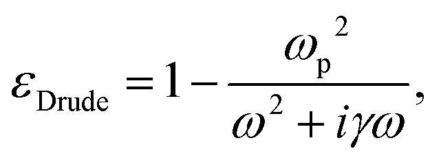
The interaction between a metallic nanoparticle and the incident light can lead to an increased photonic LDOS in the vicinity of the structures, leading to changes in the optical properties of nearby molecules such as the spontaneous emission rate.22 Thus, these interactions can be effectively used in the enhancement and manipulation of light interaction with emitters, opening a variety of applications in biosensing.18,23 In addition, the resonant frequency of the surface plasmons is adjustable based on the size, geometry, dielectric environment, material composition (see Fig. 1a and b) and separation distance of the metallic structures and will lead to opportunities in designing specific structures for specific applications.24
 | ||
| Fig. 1 The fundamental optoelectrical properties of metallic nanostructures and graphene. Schematic illustration of a localized surface plasmon resonance (a). Plasmon tuning ranges of the common plasmonic metallic materials, Au, Ag, and Al (b). Extinction spectra of a gold monomer, and gold hepatmers with different interparticle gap separations (c). Schematic of an ion-gel-gated graphene monolayer on a fused silica substrate covered by ion-gel and voltage biased by the top gate (d). Fermi level variation of single-layer graphene modulated with electrical field (e). (a) is adapted from ref. 46 with permission from The Royal Society of Chemistry, Copyright (2016). (b) is adapted from ref. 47 with permission from American Chemical Society, Copyright (2014). (c) is adapted from ref. 25 with permission from American Chemical Society, Copyright (2010). (d) and (e) are adapted from ref. 40 and 39 with permission from Springer Nature, Nature Photonics, Copyright (2018) and American Chemical Society, Copyright (2011), respectively. | ||
Transition from single plasmonic particle to multiple particles arranged in complex geometries leads to strong interactions of plasmons in metallic nanostructures assemblies that can help with the optimization of plasmon resonance frequencies for applications in the field of plasmonic sensors. For example, in the case of pillars, as illustrated in Fig. 1c, the optical response of the pillars is determined by the near-field interaction between neighboring elements. In the gold monomer, common dipolar plasmon resonances are observed, while in the heptamers with small enough interparticle gap distance, the transition from isolated to collective modes is observed. In addition, a pronounced Fano resonance dip is observed that can be characterized by destructive interference of oscillating plasmons of the central metallic structure and the ring-like hexamer surrounding it. The existence of the Fano resonance in metallic nanopillars aids tuning the plasmon resonances for enhanced biosensing.25
In order to understand the interaction of the incident electromagnetic field with the plasmonic nanostructure pillars in close proximity, first, we demonstrate the strong electric field induced by the field of the light in the confined surface of the nanoparticle/disc. Consider an incident laser beam with specific electric field E0 shining on the surface of a round-shaped metallic nanoparticle/disc in an array. The metallic nanostructure first concentrates the light to an extremely small (subwavelength) volume, which gives rise to a strong electric field confinement at the surface of the single metallic disc, Esurface, which is greatly enhanced compared to the initial electric field of the beam, E0.18 The electric field at the surface of single metallic nanoparticle/disc is derived using the following eqn (1), and strongly depends on damping by absorptive processes within the metal nanostructure, such as electron–phonon oscillations and electron surface scattering, which can be described by the imaginary part of the dielectric function.
 | (1) |
 | (2) |
By bringing two metal nanoparticle/disc in proximity of each other, the nearfield of one can interact with the other one. In a way that the electric field felt by each nanoparticle/disc is equal to E0 + Enf instead of E0. As a result of this interaction the two, neighboring nanoparticle/disc will be coupled. This coupling of oscillations is called plasmon coupling and is polarization-dependent which can be manifested in shifts of wavelength in absorption spectra.26,27 Consider a polarized incident light with direction parallel to the inter-particle/disc axis shine on nanoparticle/disc pillar, the plasmon resonance will be red-shifted relative to the resonance of individual nanoparticle/disc. Lowering the gap-size between the particles/discs will results in larger red-shift. This polarization dependence of the plasmon coupling in nanostructure pillars is analogues to the absorption spectra shifts in organic molecules upon oligomerization.25
While metals such as Au and Ag have been extensively studied as plasmonic materials and have been reviewed elsewhere,28–30 novel materials that exhibit two-dimensional plasmons such as graphene are currently explored as potential plasmonic materials in biosensors.31 Graphene addresses issues such as limited tunability and large ohmic losses in coupling of electromagnetic waves to the charge excitation at the surface of sub-wavelength metallic nanostructures and offer tighter confinement and higher tunability via electrostatic gating compared to common metallic nanostructures along with longer propagation distances.32,33 Graphene plasmons have vastly attracted investigations both in the area of fundamental properties31,34,35 and their potential applications in biosensing.36
An undoped graphene monolayer has a constant broadband absorption equal to 2.3%.37,38 The optical absorption of graphene is tunable via electrical gating by applying a voltage to shift the electronic Fermi level. Fig. 1d shows a representative schematic demonstration of a fabricated ion-gel-gated monolayer graphene transistor covered by ion-gel and voltage biased by a top gate. In this example, gold was used as electrode material and fused silica was used as substrate. Fig. 1e represents a schematic diagram demonstrating the modulation of the Fermi level of single-layer graphene via an applied electrical field. The positions of the Fermi level and Dirac point are equal in undoped monolayer graphene. When a negative/positive gate voltage is applied, the Fermi level of graphene will shift lower/upper vs. the Dirac point, which results in negative/positive doping of the graphene monolayer. This further opens up the possibility of controlling of its optical properties in selected spectral regimes.39,40 Highly doped graphene has been recently investigated as a potential plasmonic material candidate because of its unique, tunable electrical properties.41 It has shown promising plasmonic properties in the mid-infrared and terahertz spectral regions.41–43 Graphene plasmon polaritons features stronger light–matter interaction, slow light propagation, high Purcell factor, and single photon non-linearities that have been fundamentally reviewed previously.31,34,44 Tunable optical properties of graphene that enable tunable plasmonic properties of this material via the applied gate voltage leads to tunable light–matter interaction which can be used in ON/OFF switch sensors.45
3. Potential for improvement of plasmonic biosensors for applications at the point of need
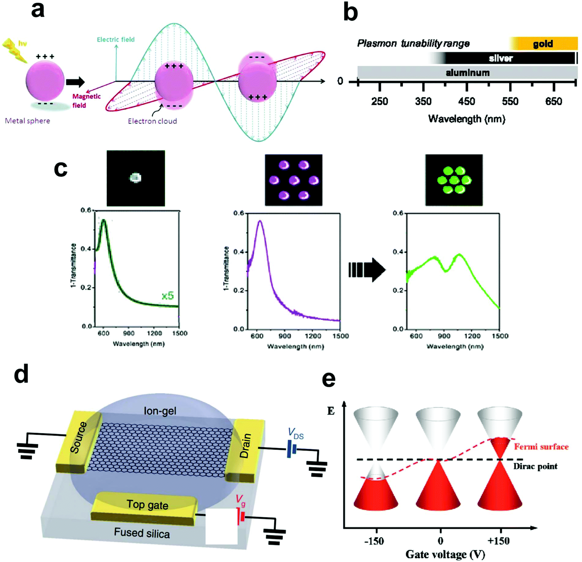
Over the past decades, plasmonic biosensors have been studied and their performance characterized for numerous applications in health, food safety, and environment monitoring. One particular area of interest is for point of need (PON) applications. PON applications, which include point of care, are applications where diagnosis or monitoring is needed, with recommendations for potential treatment, remediation, or follow up to a more specialized institution. Low cost, high sensitivity and specificity, fast response, possibility for multiplexed detection,48 and relative simplicity in operation make plasmonic biosensors more attractive for these applications over traditional biosensors.The development and use of plasmonic biosensors for PON applications involves multiple steps, such as design and fabrication of substrates (Fig. 2a), functionalization of substrates and preparation of samples, and detection of a signal indicating the presence and concentration of the analytes (Fig. 2b). The working principles of these biosensors at each of these steps are described below, together with opportunities to improve their performance.
 | ||
| Fig. 2 Schematics of biosensing based on plasmonic materials. The preparation of measurements: functionalized substrates (based on antibody/antigen, aptamers, and molecular imprinting) of different materials and structures (a) and various detection methods (b). | ||
3.1. Basic concepts of biosensing
To evaluate the performance of biosensors, basic concepts are commonly used such as sensitivity, selectivity, receiver operating characteristic curve, limit of detection, figure of merit, and reproducibility. Here we provide a table summarizing their general definitions and the specific meaning in the context of plasmonic biosensing. The method of quantification (if applicable) is then provided in each specific case. In addition to these factors, specific factors related to plasmonic biosensors can be defined, such as the SERS enhancement factor, which is also discussed in the table below.3.2. Materials
The selection of plasmonic materials as a medium for generating SPR or LSPR plays an important role in biosensing. As mentioned above, plasmonic phenomena emerge when light interacts at the interface between metals and dielectric materials. In order to choose the optimum plasmonic material, several factors need to be considered: the loss, the reactivity, the resonant region (plasmon tuning range), and the tunability of optical properties.Considering the drawbacks of metals, researchers are also searching for other materials as the substitute of metals. Due to low carrier concentration, it is difficult to observe plasmons in NIR or visible range for semiconductors.55 However, graphene can potentially address this limitation due to their unique plasmon dispersion properties that describe the relation between carrier concentration and Fermi energy,55 which can be tuned by doping. Graphene has a very high absorption capability with linear dispersion of Dirac fermions enabling changing optical properties using electric gating.41,57 Koppens et al. showed that in doped graphene the electrical and mechanical properties entail partly from its Dirac fermions charge (charge carriers at zero effective mass), which allow micrometer-range travelling of charges without scattering. The surface plasmons bound to the surface of doped graphene facilitate strong light–matter interactions due to very small plasmon confinements in relation to the diffraction limit. In addition, extremely strong light–matter interaction is attainable at the quantum level.31 Thus, an advantageous tunable surface plasmon spectra with hundreds of optical cycles can be achieved. With sufficient large doping, it is possible to achieve low losses at NIR frequencies.58
Low et al. reviewed approaches to chemically, electrically and solid electrolyte gating of graphene to achieve higher concentration of free carriers per atom and using plasmonic graphene as substitute for plasmonic noble metals in various applications such as modulators, notch filters and mid-infrared photodetectors.43
3.3. Structures
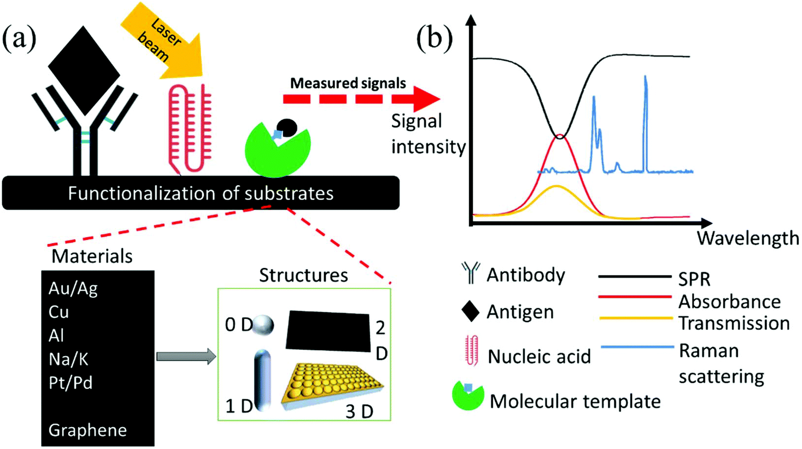
The plasmonic properties of the substrates in terms of the resonance frequency and strength of the electric field are affected not only by the materials but also by the structures of substrates such as size, shape and geometry. As mentioned in eqn (2), the electric field near the surface is related to polarizability, which can be calculated using the dielectric function of medium and the size of the substrate.59 Recent research has been devoted to the study of substrate structures, from 0D to 3D (Fig. 2a and3), from nanoparticles with different shapes (spheres, semi-spheres, pyramids, nano-stars, etc.) to the deposition of plasmonic materials on a series of substrates with different nanostructures. | ||
| Fig. 3 EM images of AuNPs deposited on carbonized paper (a), side view of a SERS sensor consisting of nanoporous PS-b-P2VP nanorods functionalized with AuNPs connected to a nanoporous PS-b-P2VP membrane (b), Au nanorods (c), MoS2/silver nanodisk hybrid structure on a Si/SiO2 substrate (d), and Au-deposited quasi-3D plasmonic crystal (e). (a) is adapted from ref. 60 with permission from Elsevier Copyright (2017). (b) is adapted from ref. 99 with permission from John Wiley and Sons, Copyright (2017). (c) is adapted from ref. 69 with permission from The Royal Society of Chemistry, Copyright (2013). (d) is adapted from ref. 100 with permission from American Chemical Society, Copyright (2016). (e) is adapted by from ref. 81 with permission from Springer Nature, Nature Communications, Copyright (2011). | ||
When working with a nanosphere with a certain radius, the plasmonic properties are easy to understand by calculating the polarizability, which is related to the electric field. Among nanoparticles, noble metals such as silver nanoparticles (AgNPs) and gold nanoparticles (AuNPs) are most usually used since they can enhance SERS signals more significantly.13,60,61
When nanoparticles are designed in other shapes that are more complex, such as nanostars nanofingers,62,63 and nanorods,64–68 the plasmonic properties of the substrate are influenced by the shapes as well. For example, the plasmonic properties of nanorods depend very much on the ratio of the semi axes and head shape,69 while the characterization of nanostars and nanofingers have to consider the tips and the center parts at the same time.29 On the other hand, core–shell structures,65,70–72 can be considered as a single sphere with an equivalent radius.73
Other 2D structures include graphene and graphene oxide (GO), which show promising potential for SERS technology due to the high ratio of surface to volume, good electrical performance, and high affinity for some molecules.75,76 Graphene grown on Cu foils was used as the deposition substrate for Au nanoislands, which increases the enhancement factor.77
In addition to graphene, silicon is also considered as a potential substrate for plasmonic materials. For example, silicon nanowires (SiNWs) exhibit a number of unique properties such as the biocompatibility, the fast response and the reproducibility that make it ideal alternative for the biosensors.78
Alternatively, 3D structures can be designed and fabricated by combining nanoparticles with 3D substrates and templates. These materials can be made by deposition or other methods. For example, AgNPs or AuNPs can be deposited on paper/paper fiber,90,91 silicon wafer,89 glass,92 or biological materials with unique structures such as cicada wing segment with patterned protrusion,93 dragonfly wing with disordered morpha,94 and Mytilus coruscus shell offering several types of micro/nano-structures,93 crystal biosilica diatoms95–97 and even on modified Nafion leafs.95 In addition to deposition, metallic nanoparticles can also be encapsulated into mesoporous silica structure.98 In these case, the plasmonic modes rise from the electromagnetic coupling of nanoparticles oriented on the nanostructured substrates.73
3.4. Functionalization of substrates
Due to the nature of the signal enhancement, which depends on the electric field near the plasmonic structure, the signal intensity is very sensitive to the distance between samples and substrates. Therefore, careful design of the surface chemistry is very important in the detection of analytes of interest. Substrates can be classified into two broad types according to whether or not they are utilizing a biorecognition element: functionalized and non-functionalized. Functionalized substrates use molecular interactions for specific detection (such as antibodies, aptamers, or other small molecules designed to specifically attach to the targeted analyte), and the analyte binding to the biorecognition element will cause a change in the detected signal.105 There are mainly three main types of functionalization based respectively on antibody, aptamer, and molecular template. Antibody/antigen-based functionalization is based on the specific noncovalent binding of the antibody to the molecule of interest. To further improve the sensitivity, a secondary antibody construct can be applied to amplify the detection signal.106 The drawback of this approach, though, is the fact that the analyte may be localized, after binding, too far from the plasmonic substrate to be detected. Aptamers, on the other hand, are oligonucleotides that have the ability to fold into smaller 3D structures that enable them to specifically bind to the analyte of interest via electrostatic interactions and localize the analyte closer to the substrate. However, these two methods mentioned above are usually not suitable for detecting small biological molecules.107 One reason for this is the fact that the recognition site in the biorecognition element may be at a distance from the surface of the plasmonic structure. In this case, the signal generated by the small target molecule decays rapidly with the distance, as described by eqn (2), and the signal may be too weak to be detected. An alternative approach for small molecule detection is by using molecular imprinting technologies. The template molecule (the analyte to be detected) is used to generate a specific shape hole in the template polymer leading to specific detection of the analyte.107Another method to address the limitation of sensitivity is the use of non-functionalized substrates. In this approach, the molecules of interest may bind directly to the plasmonic structure and generate a measurable signal. Multiple binding analytes may pose a problem in this case that limits the specificity of detection. The advantage though is the fact that higher enhancement factors can be achieved due to closer proximity of the analyte to the plasmonic substrate.108
3.5. Detection methods
Based on the detection method, plasmonic biosensors can be divided into two types: SPR-based on flat thin film and LSPR-based including scattering detection such as SERS, and absorption, transmission, reflectance detection. In addition, fluorescence based detection also draws a lot of attention.109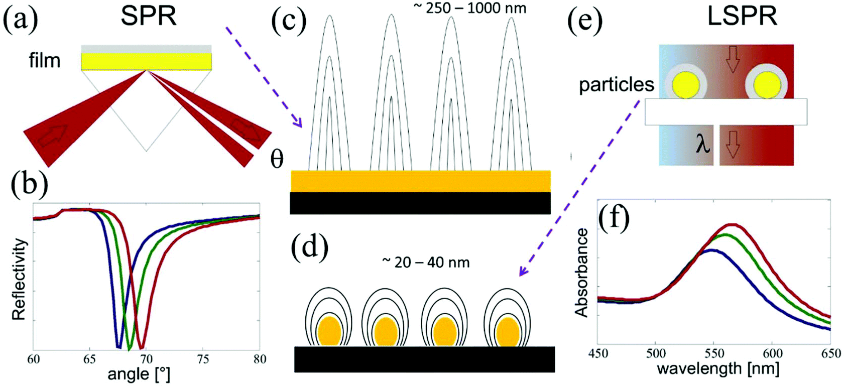 | ||
| Fig. 4 The schematic of the mechanism of SPR (a–c) and LSPR (d–f). (a), (b), (e) and (f) are adapted from ref. 120 with permission from Elsevier, Copyright (2016). | ||
Biosensing methods based on SPR use total internal reflection of incident light at the metal-dielectric interface and the generation of SPPs at certain angles. While several configurations are possible, for an SPR system based on a prism coupler, the wavevector of the evanescent field in response to an electromagnetic wave of wavelength λ incident at an angle θ propagating along (parallel to) the interface of prism-metal is related to the refractive index of the prism and incident angle.114
 | (3) |
Surface plasma wave (SPW) is an electromagnetic wave that propagates along the interface between metal and dielectric. The wavevector can be described as eqn (4):115
 | (4) |
Resonance occurs when kSP = kevan, thus, the incident angle, or the SPR angle necessary for resonance occurrence can be calculated by the equations mentioned above:
 | (5) |
To improve the sensitivity of SPR biosensors, i.e., to increase the change in SPR angle or wavelength results from the change of refractive index due to the absorption of analyte on the interface of metal and dielectric,116 substrates as the sensing platform play an important role, as indicated in eqn (5), where the dielectric functions of the metal is involved. Gold and silver thin films are most commonly used metals due to their low loss compared to other metals. Graphene also shows enhancement on SPR sensing.117 Another way to improve the performance is to coat the substrates with dielectric layer.118 On the other hand, SPR signal can also be amplified by utilizing plasmonic nanoparticles. By binding nanoparticles, such as Au, the detected SPR signal can be enhanced due to the localized and propagating surface plasmon.119
LSPR. Different from traditional SPR sensors that are based on metallic films, LSPR is generated usually on metallic nanoparticles or structures that generate localized electromagnetic fields where the decay length is much shorter (Fig. 4(d–f)). This confinement enhances the electric field at nanoscale around the metal nanoparticles, and such LSPR is sensitive to molecular binding especially for some small biological molecules.121
Similar to SPR, for LSPR and SERS, the localized electric field relies on the dielectric and plasmonic nanostructures.20,128 The extinction spectrum for a sphere (with diameter a) can be described as below:20
 | (6) |
Both SPR- and LSPR-based techniques show potential to be used towards PON applications due to their high sensitivity and specificity. From a practical perspective, more advances in fabrication methods are needed to reduce the fabrication complexity, achieve better defined and controlled nanostructures. Moreover, the use of portable spectrometers that can now be on the size of a cell phone also makes these techniques better candidates for PON applications.
Fluorescence biosensors utilize exogenous fluorophores to record and measure analyte binding events. They provide high sensitivity and specificity in the presence of interfering substances, but require additional preparation steps (labeling with the fluorophore), which may in certain situations increase the complexity of the biosensor, which may decrease its possibility to be used in PON applications.
SEIRAS utilizes the enhancement of the absorption of infrared light by the molecule when the molecule is adsorbed on nanostructured metal films.133 The enhancement is attributed to the excitation of the localized surface plasmon resonance, the orientation of the vibrational dipole of the analyte, and the change of the polarizability of the analyte. But the main mechanism is usually considered as the electromagnetic enhancement from the plasmon resonance excitation of the metallic film.134
The most commonly used sensor configuration for SEIRAS measurement is known as metal underlayer configuration, where the metallic layer is under the sample but on the supporting substrate. With this arrangement, the analytes can be measured either in transmission configuration or attenuated total reflection (ATR) configuration. For transmission measurements,135 the thickness of the metal film is less than 10 nm, allowing for a large portion of the light to be transmitted, while for ATR configuration the thickness can be up to a few hundred nanometers.
As a surface sensitive technique, SEIRAS is commonly used for near-field monolayer analysis, especially for the functional and structural study of membrane proteins.134 However, considering the rapid decrease of signal with the distance from the surface, the analyte has to be tethered extremely close to metal surface. Therefore, to improve the enhancement, molecules can be modified with high affinitive groups to metal surface such as thiol group or carboxyl group.134
However, applications to the measurement of analytes in solutions are usually challenging due to the low infrared absorption of the analyte and the interference of the strong absorption band of water. Recently, plasmonic nanoantennas were designed and fabricated to address these problems by enhancing the absorption. For example, Naomi J. Halas et al. designed antennas consisting of bowtie-shaped nanostructure with a sub-3 nm gap, which confine the mid-IR radiation and yield a high enhancement factor theoretically up to 107 for the SEIRA signal.136 Moreover, Hatice Altug's group has recently reviewed the concepts and the engineering of the plasmonic nanoantennas.137 This group has also reported a platform for molecular barcoding with pixelated dielectric metasurfaces138 and a sensor utilizing Au nanoantennas with near-field enhancement up to 1000 fold for the amide and methylene infrared bands, which allows for resolving the interaction of lipid membranes with different polypeptides in real time and distinguishing multiple analytes with high sensitivity.139 These developments provide unique opportunities for fingerprinting of various molecules complementary to Raman spectroscopy.
SEIRAS offers lower enhancement factor compared to SERS, which makes it less competitive towards PON applications. It still offers high sensitivity, thus for some applications with moderate demand for sensitivity, it is still applicable.
TERS. TERS is a special approach in SERS where the enhancement happens only at the tip of plasmonic cantilever. The mechanism of TERS enhancement is similar to that observed in SERS and is due to localized electromagnetic filed and chemical enhancement. The metallic nanotip is responsible for generating the electromagnetic field that is needed in Raman enhancement and allows simultaneously for high spatial resolution, while in other approaches such as SERS the plasmonic substrates with rough surface allows for field enhancement but no increased spatial resolution. The optical setup for TERS detection combines a typical micro-Raman system with a high-NA objective and an AFM controller to align the metallic nanotip on the sample surface within the laser focus.140 As a sensitive spectroscopy technique at the nanometer scale, TERS allows for the identification and characterization of analytes such as biomolecules or bioparticles. For example, Deckert's group exploited this technique for the discrimination of two viruses at single particle level by collecting TERS spectra and then classifying them with chemometric methods.141 Meanwhile, they also performed the identification of DNA,142 where TERS signal obtained with a silver tip and gold substrate can reach sub-nanometer resolution that enables the demonstration of the sequencing of single-stranded DNA molecules. This further indicates that TERS has the potential for high resolution Raman imaging of nanostructures and for the sequencing of other biopolymers of interest such as RNA and polypeptides. Lagugné-Labarthet et al. also utilized TERS to investigate DNA in different environments (such as free or in plasmid) and achieved a spatial resolution down to 8 nm.143 In addition to the application to bioanalytes, they also explored the characterization of biominerals via TERS, such as the interactions of the phosphoprotein osteopontin (OPN) with calcium oxalate monohydrate (COM) crystals.144 In this last application, TERS was uniquely able to help understand the competitive processes of COM growth and inhibition by OPN. Furthermore, TERS shows promising potential for the diagnosis of Alzheimer's disease by distinguishing the natural Ab1–42 fibrils (wild type) that are related to Alzheimer's disease from two other toxic mutants, i.e., L34T and oG37C.145 Since the proportion of amino acids in these three peptides is similar, it is very critical to examine characteristic Raman amide I and amide III bands of which the intensities are different in these peptides.
Compared to SERS, the enhancement factor of TERS comparable but with a higher spatial resolution since it addresses the issue of optical diffraction limit of spatial resolution observed in SERS.146 While TERS provides the above-mentioned advantages vs. SERS, it is complex, expansive, and complicated to use, and therefore not suitable for PON applications.
Single molecule detection has been achieved for SERS detection, enabling a more profound and fundamental understanding the interaction between the plasmonic surface and the analyte. Moreover, it allows for high sensitivity (low LOD), which is essential for the development of biosensors. Single molecule detection is possible when individual molecules are captured and detected in a confined volume, or when sparsely distributed molecules are detected in imaging mode. Fluorescence based techniques are often used due to the availability of strong signals (large quantum yield) in the presence of a dark background.147 Single molecule SERS detection has also drawn a lot of attention during the past decades due to the high enhancement factor within the hot spots. Compared to single molecule fluorescence detection, single molecule SERS avoids the labeling with fluorophores or dyes. Meikun Fan et al. optimized the distribution of AgNPs aggregates evenly on glass surface, used as SERS substrate, and achieved nearly single molecule detection.148 Another way to achieve (near) single molecule detection is to generate hot spots that capture a single molecule such that the signal from this molecule dominates the signal from neighboring molecules due to much stronger enhancement.149 In addition, research has shown that SPR-based techniques show potential for single molecule detection by reducing the collection area using a smaller aperture.150 The ability to image single molecules by SERS has been recently exploited for the development of biosensors. The main advantage comes from the fact that the LOD can theoretically become as low as one single molecule, as long as a calibration curve can be generated for quantification of the signal. In this case, plots of number of pixels that exhibit SERS signal (or alternatively the total intensity of those pixels) versus the concentration may provide the means for the quantification. However, elaborate sample preparation methods need to be used, as well as expensive and complicated detection schemes need to be applied to record the signal, which makes this technique unsuitable to PON applications.
Chiral plasmonics. Chirality refers to the asymmetry property of some biomolecules, such as some amino acids and carbohydrates, which are not superimposable with their mirror images and only exist in one handedness. This property can induce a phenomenon called circular dichroism (CD) that refers to different optical responses of the chiral structures to right- or left-handed circularly polarized light (RCP and LCP).151 Techniques based on this phenomenon have emerged in recent years, such as CD spectroscopy, which measures the difference of the absorbance between left- and right-circularly polarized light. CD spectroscopy can be used for structural identification, chiral sensing, and medical diagnosis of biomarkers of interest.152 However, the chiral optical response of natural molecules is typically weak, which makes it challenging for CD spectroscopy to become mainstream.
It has been shown that the CD spectroscopy signal can be enhanced when the chiral molecule of interest is in the vicinity with metallic nanoparticles due to near field enhancement and it is known as plasma induced chirality.152 In addition, when the plasmonic nanoparticles are arranged in chiral geometries, strong plasmonic chirality is generated. There are already review articles discussing the fundamental and progress in chiral plasmonics.153,154 We would like to comment here that chiral plasmonic biosensing is now still in a development stage. Theoretical and experimental studies showing a more comprehensive understanding of this phenomenon are needed for designing chiral plasmonic biosensing systems with better reproducibility. Thus, while possible, it is likely too early to apply chiral plasmonics in PON applications.
4. Applications
Plasmonic materials are applied in many different biosensing areas. Table 1 shows a brief summary based on reported applications within the past 5 years. We review publications aimed at the characterization of substrates and (bio)materials, as well as applications to environment monitoring, diagnosis, and food safety. We highlight the analyte of interest, whether or not they were functionalized, detection methods that were used, the substrates used in these measurements, as well as the sensitivity, specificity, ease of fabrication, response and cost (if applicable).| Concept | General definition | Plasmonic biosensor | Calculation |
|---|---|---|---|
| Abbreviation: LOD: limit of detection; P: positive; N: negative; TP: true positive; TPR: true positive rate; TN: true negative; TNR: true negative rate; FP: false positive; FN: false negative; ROC: receiver operation characteristic; FoM: figure of merit; FWHM: full width at half maximum; SD: standard deviation; RSD: relative standard deviation; CV: coefficient of variation; EF: enhancement factor. | |||
| Sensitivity | For medical diagnosis: the probability of detecting the analyte (TPR) | LOD, or How the measured signal changes in responding to varying concentration of the analyte | TPR = TP/P for medical diagnosis, or the slope of the calibration plot |
| The term is also used as the minimum concentration of the analyte that can be detected | |||
| Specificity | For medical diagnosis: true negative rate | The biosensor is able to detect and differentiate the analyte of interest in the presence of other interfering substances | TNR = TN/N for medical diagnosis |
| The ability to distinguish the analyte in presence of other components | |||
| ROC | A tool to evaluate the classification performance | The performance balance between sensitivity and false positive rate | ROC curve is true positive rate versus false positive rate |
| LOD | The lowest quantity of the analyte that can be detected reliably | The minimum quantity/concentration of the analyte that can be detected reliably | The ratio of 3 times SD of blank to the slope of calibration plot49 |
| FoM | A factor used to characterize the performance of a device, or materials, etc. | The parameter that can be used to characterize the biosensing performance such as sensitivity, LOD etc. | LSPR: The sensitivity of the refractive index in terms of change in resonance divided by resonance linewidth |
| SPR: Sensitivity (slope) divided by FWHM | |||
| Reproducibility | The consistency of measurements with same methodology | The ability to obtain identical measurements from sample to sample, time to time, spot to spot | RSD or CV |
| EF | The enhancement of SERS signal compared to Raman signal | The parameter to evaluate the enhancement of the Raman signal in the presence of plasmonic structures | The ratio between the signal detected in the presence of the plasmonic materials to the signal detected in the absence of it |
4.1. Characterization of substrates and (bio)materials
There are numerous studies dedicated to the characterization of plasmonic substrates and materials before these can be applied to any area of application. These studies provide a good indication about the performance for potential application and allows for further optimization for targeted real applications. Based on the specific area of application, the analytes include proteins, DNA, bacteria, viruses, and other biological particles such as exosomes.13,155For different detection methods, certain test molecules are generally used for the characterization of plasmonic substrates. For example, 4-ATP and Rhodamine 6G are normally used as probe molecules for substrate characterization for SERS.61,91 With these test molecules, the performance of the substrates can be characterized either by sensitivity (limit of detection), or by the enhancement factor. The performance of the substrates will be compared to normal Raman measurements to show the magnitude of surface enhancement due to the plasmonic nanostructures designed. On the other hand, to characterize an SPR system, which is highly sensitive to molecular interactions on the surface of the sensing substrate,111 researchers focus on the characterization of binding events such as antigen–antibody interactions, IgG examinations, or other types of specific molecular interaction.116
The development of substrates should consider both the analytes as well as the detection methods. For larger molecules, such as proteins, the development of biosensors needs to take into account the ability to capture the analytes into the vicinity of the active part of substrates for higher sensitivity.156 For SPR-based methods, by selecting better materials, such as Au or Ag, adjusting the thickness of sensing film, coating with other materials or incorporating nanoparticles to combine LSPR, higher sensitivity can be obtained.104,157 As for LSPR-based detection, such as SERS, as discussed before, in addition to the materials used, the fabrication of different shapes of nanoparticles, or nanostructures should be focused to achieve higher EF or higher sensitivity by generating hot spots.80
4.2. Environment monitoring
The importance of monitoring the environment is evident with the increasingly serious problems related to the pollution of water and air. The development of biosensors can facilitate the detection of pollutants in the environment in a direct and reliable manner. The biosensors used for environmental monitoring are mostly focused on pesticides that are used for crops or fruits, heavy metals in water that cannot be degraded, pathogens such as bacteria, and other chemicals that are potentially toxic or dangerous such as explosives.64,92,158 For the detection of these pollutants in real life, it is crucial to develop biosensors that can achieve rapid measurement of samples, and easy accessibility for some situation such as low resources environments.5,89,115To improve the performance of the substrates for plasmonic biosensing, it is necessary to bring pollutants as close as possible to the surface of the plasmonic active parts. One way to achieve this is by functionalizing the substrates with specific recognition elements or by designing structures to allow for the easy binding of analytes.159 On the other way, considering the chemical structures of analytes of interest, plasmonic materials with higher affinity to analytes should be considered. For example, AuNPs show high affinity to dithiolcarbamate pesticides and SERS biosensors based on AuNPs have been reported for their detection.160
4.3. Diagnosis for human health
Monitoring health at the point of need is one of the most significant problem in our world, as it can lead to early diagnosis, help understand disease progression, and provide data that can be used to develop an optimal treatment scenario. Plasmonic biosensors are good candidates for these applications as they have the ability to detect analytes of interest such as biomarkers related to diseases.11 By quantifying the biomarkers, specific health-related information can be obtained. Many biomarkers (antibodies, proteins, nucleic acids, and enzymes etc.) are the potential analytes to be monitored for the diagnosis of diseases, such as Alzheimer's, diabetes, and cancer.60,86,161,162 In addition, they can also be used for drug screening.163To capture these analytes from biofluids, specific receptors such as antibodies, or ligands are immobilized on the sensing substrates to bring the analytes closer to the sensing surface.62 In addition, tags or probes are also introduced for the purpose of improved detection. Therefore, the substrates should be designed to allow functionalization and tuning of these receptor elements.132 Consequently, the surface of the substrates designed for plasmonic biosensors need to consider the surface chemistry as well as the surface area to allow the immobilization of the receptors and stable binding of the analytes.164,165 Moreover, since the concentration of biomarkers is important for clinical determination, plasmonic biosensors used for diagnosis require high accuracy over the desired concentration range.166 Meanwhile, the need of diagnosis and disease progression monitoring in low resource environments, at home, in remote locations, in disaster areas, or for astronauts in space, drives the development of portable substrates or devices based on plasmonic biosensors.
4.4. Food safety
Monitoring the food quality is of global concern since food safety plays an important role in our daily life. The addition of high level of contaminants or adulterants in food could pose severe problems for our health, especially for infants. For example, high levels of heavy metals, plastic, or food additives can lead to severe health problems.167 In the application to food safety, plasmonic biosensors are generally used to detect chemical and microbial contaminants, such as the food colorants, food additives, or bacteria.168,169 Similar to environmental monitoring, plasmonic biosensors designed for food safety also require high sensitivity, simple preparation, and rapid detection.115,170For the detection of chemical components such as small analytes, the substrates can be engineered for specific binding of these analytes.65 However, for large analytes, such as proteins, or bacteria, the sensitivity of detection is typically lower171 and functionalization of substrates with specific antibodies or aptamers may be needed.172
4.5. Pon applications
To summarize, there are many factors to consider for the development and evaluation of plasmonic biosensors towards point-of-need applications. We mainly reviewed the potential improvement for plasmonic biosensors from the point of view of materials, the design of nanostructures, the functionalization of the substrates, and finally the detection methods. For these sections, the emphasis is focused on how the performance of the plasmonic biosensors are affected by the properties of substrates.When designing PON biosensors, it is important to address not only parameters related to cost, size, and stability, but also sensitivity, specificity and low limit of detection towards the analyte of interest for that particular applications. For this, significant effort is needed towards the design and preparation of the substrates in terms of the materials, composition, the shape, the size, and the structure.173,174 Particularly when there are other molecules that shares similar molecular properties as the test molecule (analyte), it is necessary to optimize the system accordingly, thus, the biosensing system can be specific towards the desired analytes.
The requirements regarding the sensitivity, specificity, and LOD are different when dealing with environment monitoring and food safety samples compared to PON applications in health diagnosis. The analytes of interest in environment monitoring or food safety are typically small molecules such as toxic chemicals,169 pesticides170 and heavy metals,64 which can be detected with LSPR-based techniques. In food safety or medical diagnosis, however, bacteria, proteins,36 nucleic acids,162 or vesicles are often targeted as biomarkers of interest besides small biological molecules. The detection of analytes with larger size or mass makes it more difficult for plasmonic biosensing since it demands immediate vicinity with substrate surface. Moreover, it is also more challenging to develop a biosensor for medical diagnosis due to the increased complexity of the sample and high variability of biomarkers for a specific disease. As a result, more careful functionalization of the substrate to immobilize target analytes needs to be taken into consideration for higher specificity in PON application. In addition, the reproducibility of detection with SERS is still relatively low, yielding to poor reliability for these applications. Better substrates are required in this case, and new developments in various labs indicate improved spot-to-spot reproducibility for certain substrates such as nanobowl arrays82 gold nanofingers,63 or nanoposts,175 among others.
It is also worth noticing that when it comes to PON applications, the development of plasmonic biosensors should consider other factors beyond sensitivity and specificity, such as the complexity of substrate fabrication and the preparation of analytes, the cost, and the response time.176 For PON applications, it is critical to balance the high cost, and/or the complexity of fabrication or preparation of the substrates. Since the sensitivity/LOD criteria varies in different areas, it is possible to compromise their quality when it is not highly necessary for either lower fabrication cost or less tedious preparation work.
For example, the synthesis of nanoparticles, as one of the simplest plasmonic structure, has been explored and improved for more than a hundred years,177 can be easily performed by a variety of methods. On the other hand, it is believed that the combination of the plasmonic materials such as the noble metal with hybrid nanostructures can enhance the SERS signal since more hot spots can be generated. However, the complexity of the fabrication of such nanostructures is also increased, thus it is important to balance the trade-off between the ease-of-fabrication and the design optimization of the nanostructured substrate. Making use of natural substances with unique structures is a promising approach to address this problem. For instance, Zhengyi Lu et al. developed an inexpensive SERS substrate by depositing AgNPs and graphene oxide (GO) on (a) Mytilus coruscus (M.c) shell offering several types of micro/nano-structures.93 Other natural materials, such as (b) the dragonfly wing94 and (c) cicada wing,178 combined with different metals and structures, are more explored. The utilization of the natural materials that can be readily obtained not only improves the ease-of-fabrication but also reduces the cost (Fig. 5).
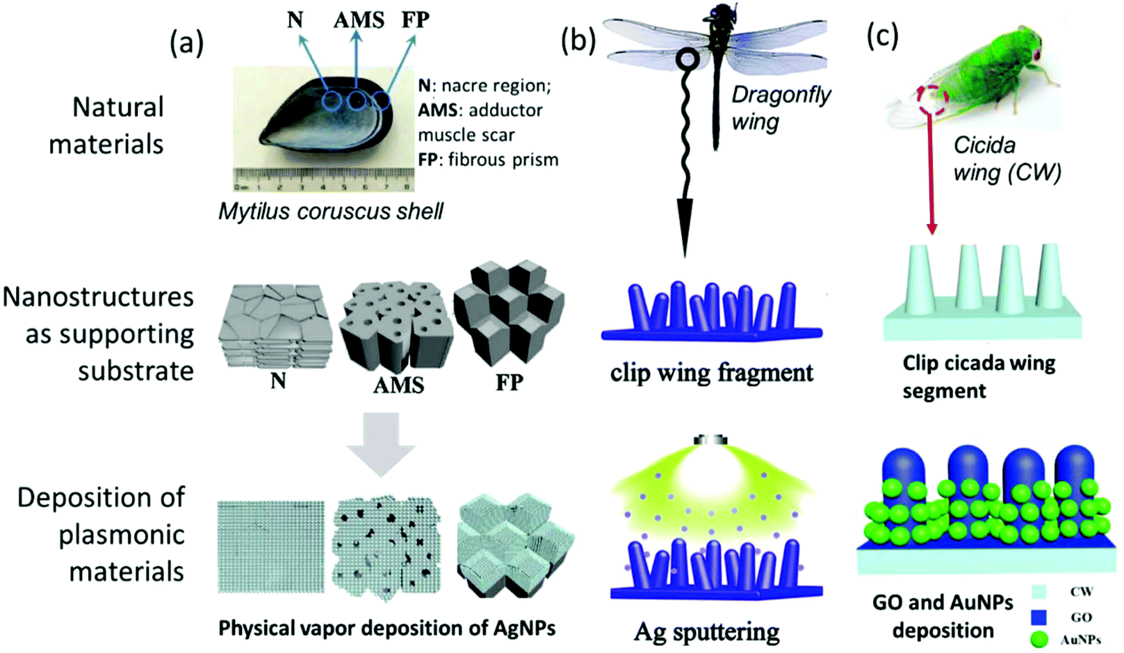 | ||
| Fig. 5 Representative examples of utilizing natural materials as supporting substrate: (a) AgNPs deposited on Mytilus coruscus (M.c) shell; (b) AgNPs sputtered on dragonfly wing; (c) Graphene oxide (GO) and AuNPs deposited on cicada wing. (a) and (b) are adapted from ref. 93 and 94 with permission under Copyright Clearance Center, Inc., Copyright (2019). (c) is adapted from ref. 178 with permission from Elsevier B.V., Copyright (2018). | ||
Another important factor for PON applications is the duration of the measurement, which is mainly determined by the detection methods. In general, the measurement of the plasmonic biosensors based on SPR/LSPR is time effective, which is determined by the incident exposure and collection time. The recording time of the SERS spectra ranges from seconds to minutes, which fulfills the demand of rapid measurement for PON applications.
The ultimate goal in studying the plasmonic biosensors that can be used for PON applications is for the development of portable devices/platforms that can be easily operated with high sensitivity and specificity, and rapid readout. Currently, there are already several SERS substrates commercially available. Most of them use gold or silver as SERS active materials, mostly AgNPs, AuNPs (RAM-SERS-AU/RAM-SERS-AG (Ocean Optics), Q-SERS™ G1 (Nanova Inc.)), or the combination of both (SERSitive). They are engineered on a supporting substrate such as glass or nanostructured Si wafer by various methods such as electrodeposition (SERSitive). The required volume for the analyte is typically very small (micro liter level). These substrates have been used for the identification of various molecules of interest such as melamine and TNT, with a low LOD.
However, several of the biosensor parameters described in Table 1, such as the sensitivity, specificity, and reproducibility, need to be further improved for successful applications in medical diagnosis.
Overall, the development of plasmonic biosensors fulfills basic requirement towards some specific PON applications regarding the sensitivity, fabrication cost, response time, etc. Even though there are still many challenges to be overcome for wider implementation, they show promising potential for future applications towards PON applications (Table 2).
| Application | Analyte | Functionalization | Detection | Substrate/material | Sensitivity | Specificity | Response time | Ease of fabrication | Cost | Ref. |
|---|---|---|---|---|---|---|---|---|---|---|
| Abbreviations: R6G: rhodamine-6G; PABT: paminobenzenethiol; 4-ATP: 4-aminothiophenol; OAD: oblique angle deposition; ATT: 3-amino-1,2,4-triazole-5-thiol; LFA: lateral flow assay; DOX: doxorubicin; Nano-DEP: nano-dielectrophoretic; AFP: α-fetoprotein; IgG: immunoglobulin G; CEA: carcinoembryonic antigen; PA: picric acid; PSA: prostate specific antigen; NTO: 3-nitro-1,2,4-trizazol-5-one; PPi: pyrophosphate; DTPA: diethylenetriaminepentaacetic acid; PMMA: polymethyl-methacrylate. | ||||||||||
| Characterization of substrates and (bio)materials | R6G and graphene for test | None | SERS | AgNPs arrays prepared by magnetic sputtering and thermal annealing process on silicon wafers | Non-applicable | Not reported | High temperature (500 °C) required for thermal annealing process | Low | 179 | |
| R6G | None | SERS | Paper with different porosities decorated with Ag nanostars | 11.4 ± 0.2 pg | Non-applicable | Min | Simple (chemical reduction + wax ink printing on paper) | Low | 91 | |
| Escherichia coli O157:H7 | Au nanorods functionalized with 4-ATP and ATT and antibodies | SERS | Nano-DEP microfluidic device. Bio-conjugated AuNPs as SERS probes. DEP force to trap cells. | 10 colony-forming unit per mL | High specificity from non target strains | Sec | Long time (19 h stirring during synthesis of AuNRs) | Low | 155 | |
| Low molecular weight molecule (glycerol) | None | SPR | Hyperbolic metamaterials: 16 alternating thin films of gold and aluminium dioxide (Al2O3) | Ultra low molecular mass of 266 Da | Non-applicable | Not reported | e-beam lithography; photoresist coating | Low | 104 | |
| Recombinant protein A/G and goat anti-mouse IgG | None | Mid-IR spectroscopy | Graphene nanoribbon arrays | Chemical bond specificity | Not reported | Chemical vapor deposition to grow Graphene | Medium | 36 | ||
| Thrombin | Thiol-modified thrombin aptamer was attached onto AuNPs/Fe3O4 | LSPR/absorption | AuNPs loaded on magnetic Fe3O4 nanoparticles | 200 pM | High selectivity of thrombin aptamer | Not reported | Simple | Low | 156 | |
| The proposed meta surface architecture provides a unique platform to selectively detect aromatic ring structure biomolecules | None | SPR | Graphene-coated Au film | 1 × 10⁻¹⁸ M; 1 × 10⁻¹⁸ M; 10−18 M | Non-applicable | Not reported | High temperature (1000 °C); chemical vapor deposition. | Medium | 157 | |
| Environment monitoring | Explosives: such as PA and NTO | None | SERS | 3D biomimetic superhydrophobic Ag micro/nano-pillar array surface, which is deposited on different types of Si arrays | R6G 10−15 mol L−1; PA 10−12 mol L−1; NTO 10−13mol L−1. | Non-applicable | Not reported | Electrodeposition of Ag sheets may require long time (7 h) | Low | 158 |
| Heavy metal ions | Diethylenetriaminepentaacetic acid-grafting to bind with heavy metal ions | SERS | Gold structure with DTPA to bind to heavy metal ions | 10−14 M | Selective metal ions detection | Tens of seconds | Long time drying (24 h); laser irradiation for patterning | Low | 159 | |
| TNT explosive | PABT (Raman signal) modification | SERS | AgNPs modified by PABT decorating silicon wafer | ∼ 1 pM | High selectivity for TNT | Tens of seconds | Simple | Low | 89 | |
| Mercury ion Hg 2+ in water | Assembling oligonucleotide probes | SERS | Silver nanorod array by OAD technique. Oligonucleotide probes are assembled through Ag–S covalent bond. | 0.16 pM | High selectivity | Second | Simple | Low | 64 | |
| Bromate in water | R6G used as a reference sample with or without bromate | SERS | Ag film made by electrostatic immobilization of AgNPs on glass slide | 0.01 μg L−1 | Non-applicable | Tens of seconds | Simple (but long time 24h dipping) | Low | 92 | |
| Diagnosis for human health | Neuron-Specific Enolase (NSE, protein) | Detection antibody-SERS probe conjugation | SERS-LFA | Au nanostar @Raman reporter@ silica (coating with 4-MBA (Raman reporter) and TEOS, then conjugated with detection antibody) | NSE detected in clinical blood plasma | Not reported | Simple | Low | 62 | |
| MicroRNA | Hybridization between complementary probes | LSPR | Gold nanoprisms attached to silanized glass | ∼10 −13 M | High selectivity | Not reported | Simple but long time preparation | 162 | ||
| Cytokines | Cytokine antibodies conjugation | LSPR/microfluidics | Au nanorods microarray | 5 pg mL −1 | Not reported | Medium (multiple processes) | 166 | |||
| Human IgG-anti-human IgG recognition | Human IgG as a recognition element for anti-human IgG | LSPR-SERS | PDMS as substrate coated with Au film in nanocup shape (nanoplatform) | 10−14 M of 4-MBA (4-mercaptobenzoic acid) | Specific for antigen–antibody binding | Tens of seconds | Simple | Low | 86 | |
| Cancer marker, Mucin-1 | Hybridized aptamer | SERS | AuNPs on paper fibers | 50 ng mL−1 | High selectivity | Not reported | Simple (but heating needs 5h) | Low | 60 | |
| Anticancer drug, DOX, assessment of DOX-dsDNA interaction (DNA damage) | None | SERS/EC | Magnetic Fe2Ni@Au nanoparticles on graphene oxide functionalized with double-stranded DNA (dsDNA) | 8 μg mL−1 | High selectivity | Not reported | Auto clave long time (19 h) | Low | 163 | |
| Multiple label-free detection: cancer biomarkers, including AFP, CEA, and PSA | None | LSPR (scattering shift) | Immune-AuNPs immobilized on glass slide | 91 fM, 94 fM and 10 fM for AFP, CEA and PSA | High selectivity | Not reported | Medium (long time stirring 10h, multiple processes) | Medium (promission for low cost) | 164 | |
| PPi, related to DNA replication | Substrate immobilized with meso-tetra(4-carboxyphenyl)porphyrin | Fluorescence | AuNRs as core with a silica shell | 820 × 10−9 M of PPi | High selectivity | Not reported | Simple but long time preparation (10 h during AuNR systhesis and 24 h for silica coating) | Low | 132 | |
| Food safety | Melamine in milk | None | SERS | Silver dendrite | 7.9 × 10 −7 M | Specific for melamine | Tens of seconds | Simple | Low | 169 |
| Melamine detection in animal feed | None | SERS | Ag nanorod array | 0.9 μg g−1 feed | High selectivity | Tens of seconds | Simple (OAD) | Low | 65 | |
| Pesticide residues such as parathionmethyl, thiram, and chlorpyrifos | None | SERS | Colloidal AuNPs decorated commercial tapes | 2.60 ng cm−2 0.24 ng cm−2 3.51 ng cm−2 | Non-applicable | Tens of seconds | Simple | Low | 170 | |
| Methylene-blue in fish | None | SERS | Ag nanoflowers sandwiched between PMMA and monolayer graphene | 10 −13 M | Change with analyte in real sample | Not reported | Slow displacement reaction and etching process | Low | 168 | |
5. Conclusions and outlook
The field of plasmonic biosensors has made great progress in recent years, which prompted many research groups to explore their potential in various fields and applications, such as environment monitoring, food safety, and diagnosis. However, taking these devices out of the lab into the field has been a difficult task, with only very few examples of use in real life applications, and in particular at the point of need. Due to their ability to absorb visible light and convert it into a heat signature, gold nanoparticles are currently used to improve the sensitivity of lateral flow assays. In order for plasmonic biosensors to expand their range of applications and become mainstream it is critical to improve their sensitivity, specificity, and reproducibility, as well as design and implement specifications that allow for their use in conditions typically found at the point of need. These include robustness, form factor, user interface, response time, and cost. The ability to connect to mobile devices for data transmission and analysis is also important.There are many factors playing an important role in designing and fabricating plasmonic substrates. In the paper, we reviewed the fundamentals of plasmonics, the optical properties of substrates, and the detection methods that are used in the measurements of molecules of interest. Specifically, we describe material properties that allow optimization towards improved detection, the structures that allow for additional tuning of material properties, the functionalization and sample preparation, and the detection methods that can be used. Other factors include the limit of detection and the incorporation of LSPR devices into multiplexed platforms that are still challenging.180 Improving the sample-to-sample reproducibility as well as reducing the sampling error is still difficult because of the limit in controlling the size, shape, and surface of the plasmonic nanostructures, especially for the Ag or Au nanoparticles.181
We also reviewed in this article practical applications. Significant progress has been made, as highlighted in this review. However, most examples currently found in the literature include tests performed in the lab under controlled experimental conditions. They describe substrate manufacturing and functionalization, report improvements in detection schemes, and demonstrate their applicability to the detection of certain analytes. One drawback is the fact that in many of the examples shown, the samples are simulated and measured in the lab, and may not necessarily provide an accurate representation of the complex situations in the field. This makes, in general, the evaluation of the potential of these sensors difficult. In conclusion, while plasmonic biosensors are not currently found in many PON applications, the increased quality of the data and exponential growth of the field demonstrates that such applications are not far away.
Author contributions
All authors made substantial intellectual contributions to the manuscript and approved it for publication.Conflicts of interest
The authors declare that the research was conducted in the absence of any commercial or financial relationships that could be construed as a potential conflict of interest.Acknowledgements
This work was financially supported by the National Sciences and Engineering Research Council of Canada (NSERC), Discovery Grant RGPIN-2018-05675 (to S.W.-H.), and G247765 and G248584 (to S.M.). The authors also thank the Faculty of Engineering at McGill University. J.L. and M.J. acknowledge the McGill Engineering Doctoral Award (MEDA).References
- J. Chao, W. Cao, S. Su, L. Weng, S. Song, C. Fan and L. Wang, J. Mater. Chem. B, 2016, 4, 1757–1769 RSC.
- J. Zheng and L. He, Compr. Rev. Food Sci. Food Saf., 2014, 13, 317–328 CrossRef CAS.
- P. Mehrotra, J. Oral Biol. Craniofac. Res., 2016, 6, 153–159 CrossRef.
- C. I. Justino, T. A. Rocha-Santos and A. C. Duarte, TrAC, Trends Anal. Chem., 2010, 29, 1172–1183 CrossRef CAS.
- C. I. Justino, A. C. Duarte and T. A. Rocha-Santos, Sensors, 2017, 17, 2918 CrossRef.
- J. R. Mejía-Salazar and O. N. Oliveira, Chem. Rev., 2018, 118, 10617–10625 CrossRef.
- L. Tang and J. Li, ACS Sens., 2017, 2, 857–875 CrossRef CAS.
- M. Oliverio, S. Perotto, G. C. Messina, L. Lovato and F. De Angelis, ACS Appl. Mater. Interfaces, 2017, 9, 29394–29411 CrossRef CAS PubMed.
- R. T. Hill, Wiley Interdiscip. Rev.: Nanomed. Nanobiotechnol., 2015, 7, 152–168 CrossRef CAS.
- J. Langer, D. Jimenez de Aberasturi, J. Aizpurua, R. A. Alvarez-Puebla, B. Auguié, J. J. Baumberg, G. C. Bazan, S. E. J. Bell, A. Boisen, A. G. Brolo, J. Choo, D. Cialla-May, V. Deckert, L. Fabris, K. Faulds, F. J. García de Abajo, R. Goodacre, D. Graham, A. J. Haes, C. L. Haynes, C. Huck, T. Itoh, M. Käll, J. Kneipp, N. A. Kotov, H. Kuang, E. C. Le Ru, H. K. Lee, J.-F. Li, X. Y. Ling, S. A. Maier, T. Mayerhöfer, M. Moskovits, K. Murakoshi, J.-M. Nam, S. Nie, Y. Ozaki, I. Pastoriza-Santos, J. Perez-Juste, J. Popp, A. Pucci, S. Reich, B. Ren, G. C. Schatz, T. Shegai, S. Schlücker, L.-L. Tay, K. G. Thomas, Z.-Q. Tian, R. P. Van Duyne, T. Vo-Dinh, Y. Wang, K. A. Willets, C. Xu, H. Xu, Y. Xu, Y. S. Yamamoto, B. Zhao and L. M. Liz-Marzán, ACS Nano, 2019 DOI:10.1021/acsnano.9b04224.
- M. Soler, C. S. Huertas and L. M. Lechuga, Expert Rev. Mol. Diagn., 2019, 19, 71–81 CrossRef CAS.
- D. B. Gupta, A. Pathak and V. Semwal, Sensors, 2019, 19, 3536 CrossRef.
- M. Kahraman, E. R. Mullen, A. Korkmaz and S. Wachsmann-Hogiu, Nanophotonics, 2017, 831 CAS.
- E. Ozbay, Science, 2006, 311, 189–193 CrossRef CAS PubMed.
- M. E. Stewart, C. R. Anderton, L. B. Thompson, J. Maria, S. K. Gray, J. A. Rogers and R. G. Nuzzo, Chem. Rev., 2008, 108, 494–521 CrossRef CAS PubMed.
- M. Born and E. Wolf, Principles of Optics, 6th edn, 1999 Search PubMed.
- S. A. Maier, Plasmonics: fundamentals and applications, Springer Science & Business Media, 2007 Search PubMed.
- V. Giannini, A. I. Fernández-Domínguez, S. C. Heck and S. A. Maier, Chem. Rev., 2011, 111, 3888–3912 CrossRef CAS PubMed.
- W. L. Barnes, A. Dereux and T. W. Ebbesen, Nature, 2003, 424, 824–830 CrossRef CAS PubMed.
- K. A. Willets and R. P. Van Duyne, Annu. Rev. Phys. Chem., 2007, 58, 267–297 CrossRef CAS.
- P. K. Jain and M. A. El-Sayed, Chem. Phys. Lett., 2010, 487, 153–164 CrossRef CAS.
- M. Cuevas, J. Quant. Spectrosc. Radiat. Transfer, 2018, 206, 157–162 CrossRef CAS.
- A. G. Brolo, Nat. Photonics, 2012, 6, 709 CrossRef CAS.
- E. Petryayeva and U. J. Krull, Anal. Chim. Acta, 2011, 706, 8–24 CrossRef CAS.
- M. Hentschel, M. Saliba, R. Vogelgesang, H. Giessen, A. P. Alivisatos and N. Liu, Nano Lett., 2010, 10, 2721–2726 CrossRef CAS.
- W. Rechberger, A. Hohenau, A. Leitner, J. R. Krenn, B. Lamprecht and F. R. Aussenegg, Opt. Commun., 2003, 220, 137–141 CrossRef CAS.
- K. H. Su, Q. H. Wei, X. Zhang, J. J. Mock, D. R. Smith and S. Schultz, Nano Lett., 2003, 3, 1087–1090 CrossRef CAS.
- W. A. Murray and W. L. Barnes, Adv. Mater., 2007, 19, 3771–3782 CrossRef CAS.
- M. Pelton, J. Aizpurua and G. Bryant, Laser Photonics Rev., 2008, 2, 136–159 CrossRef CAS.
- S. Lal, S. Link and N. J. Halas, Nat. Photonics, 2007, 1, 641 CrossRef CAS.
- F. H. Koppens, D. E. Chang and F. J. García de Abajo, Nano Lett., 2011, 11, 3370–3377 CrossRef CAS.
- I. Goykhman, U. Sassi, B. Desiatov, N. Mazurski, S. Milana, D. de Fazio, A. Eiden, J. Khurgin, J. Shappir and U. Levy, Nano Lett., 2016, 16, 3005–3013 CrossRef CAS PubMed.
- C. T. Phare, Y.-H. D. Lee, J. Cardenas and M. Lipson, Nat. Photonics, 2015, 9, 511 CrossRef CAS.
- S. Xiao, X. Zhu, B.-H. Li and N. A. Mortensen, Front. Phys., 2016, 11, 117801 CrossRef.
- S. Thongrattanasiri, A. Manjavacas and F. J. García de Abajo, ACS Nano, 2012, 6, 1766–1775 CrossRef CAS PubMed.
- D. Rodrigo, O. Limaj, D. Janner, D. Etezadi, F. J. G. De Abajo, V. Pruneri and H. J. S. Altug, Science, 2015, 349, 165–168 CrossRef CAS PubMed.
- M. Liu, X. Yin, E. Ulin-Avila, B. Geng, T. Zentgraf, L. Ju, F. Wang and X. J. N. Zhang, Nature, 2011, 474, 64 CrossRef CAS.
- R. R. Nair, P. Blake, A. N. Grigorenko, K. S. Novoselov, T. J. Booth, T. Stauber, N. M. Peres and A. K. Geim, Science, 2008, 320, 1308–1308 CrossRef CAS PubMed.
- H. Xu, L. Xie, H. Zhang and J. Zhang, ACS Nano, 2011, 5, 5338–5344 CrossRef CAS PubMed.
- T. Jiang, D. Huang, J. Cheng, X. Fan, Z. Zhang, Y. Shan, Y. Yi, Y. Dai, L. Shi and K. Liu, Nat. Photonics, 2018, 12, 430–436 CrossRef CAS.
- F. J. Garcia de Abajo, ACS Photonics, 2014, 1, 135–152 CrossRef CAS.
- A. Grigorenko, M. Polini and K. Novoselov, Nat. Photonics, 2012, 6, 749 CrossRef CAS.
- T. Low and P. Avouris, ACS Nano, 2014, 8, 1086–1101 CrossRef CAS PubMed.
- S. Thongrattanasiri, A. Manjavacas and F. J. García de Abajo, ACS Nano, 2012, 6, 1766–1775 CrossRef CAS PubMed.
- D. Jiang, X. Du, D. Chen, L. Zhou, W. Chen, Y. Li, N. Hao, J. Qian, Q. Liu and K. Wang, Biosens. Bioelectron., 2016, 83, 149–155 CrossRef CAS PubMed.
- S. Peiris, J. McMurtrie and H.-Y. Zhu, Catal. Sci. Technol., 2016, 6, 320–338 RSC.
- M. W. Knight, N. S. King, L. Liu, H. O. Everitt, P. Nordlander and N. J. Halas, ACS Nano, 2013, 8, 834–840 CrossRef PubMed.
- M.-C. Estevez, M. A. Otte, B. Sepulveda and L. M. Lechuga, Anal. Chim. Acta, 2014, 806, 55–73 CrossRef CAS PubMed.
- B. Špačková, P. Wrobel, M. Bocková and J. Homola, Proc. IEEE, 2016, 104, 2380–2408 Search PubMed.
- D. Ö. Güney, T. Koschny and C. M. Soukoulis, Phys. Rev. B: Condens. Matter Mater. Phys., 2009, 80, 125129 CrossRef.
- M. N. Gjerding, M. Pandey and K. S. Thygesen, Nat. Commun., 2017, 8, 15133 CrossRef PubMed.
- A. Boltasseva and H. A. Atwater, Science, 2011, 331, 290–291 CrossRef CAS PubMed.
- J. B. Khurgin and G. Sun, Appl. Phys. Lett., 2010, 96, 181102 CrossRef.
- P. R. West, S. Ishii, G. V. Naik, N. K. Emani, V. M. Shalaev and A. Boltasseva, Laser Photonics Rev., 2010, 4, 795–808 CrossRef CAS.
- G. V. Naik, V. M. Shalaev and A. Boltasseva, Adv. Mater., 2013, 25, 3264–3294 CrossRef CAS PubMed.
- K. Okamoto, in Frontiers of Plasmon Enhanced Spectroscopy, ACS Publications, 2016, vol. 2, pp. 247–259 Search PubMed.
- G. Robb, Nat. Photonics, 2016, 10, 3 CrossRef CAS.
- M. Jablan, H. Buljan and M. Soljačić, Phys. Rev. B: Condens. Matter Mater. Phys., 2009, 80, 245435 CrossRef.
- J. Langer, S. M. Novikov and L. M. Liz-Marzán, Nanotechnology, 2015, 26, 322001 CrossRef PubMed.
- S.-W. Hu, S. Qiao, J.-B. Pan, B. Kang, J.-J. Xu and H.-Y. Chen, Talanta, 2018, 179, 9–14 CrossRef CAS PubMed.
- Y. Bai, L. Yan, J. Wang, L. Su, N. Chen and Z. Tan, Phot. Nanostruct. – Fund. Appl., 2017, 23, 58–63 CrossRef.
- X. Gao, P. Zheng, S. Kasani, S. Wu, F. Yang, S. Lewis, S. Nayeem, E. B. Engler-Chiurazzi, J. G. Wigginton and J. W. Simpkins, Anal. Chem., 2017, 89, 10104–10110 CrossRef CAS PubMed.
- A. Kim, S. J. Barcelo and Z. Li, Nanotechnology, 2014, 26, 015502 CrossRef PubMed.
- C. Song, B. Yang, Y. Zhu, Y. Yang and L. Wang, Biosens. Bioelectron., 2017, 87, 59–65 CrossRef CAS PubMed.
- J. Cheng, X.-O. Su, Y. Yao, C. Han, S. Wang and Y. Zhao, PLoS One, 2016, 11, e0154402 CrossRef PubMed.
- C. Song, Y. Yang, B. Yang, Y. Sun, Y. Zhao and L. Wang, Nanoscale, 2016, 8, 17365–17373 RSC.
- Z. Zhang, Z. Chen, F. Cheng, Y. Zhang and L. Chen, Analyst, 2016, 141, 2955–2961 RSC.
- Z. Zhang, Z. Chen, S. Wang, F. Cheng and L. Chen, ACS Appl. Mater. Interfaces, 2015, 7, 27639–27645 CrossRef CAS PubMed.
- H. Chen, L. Shao, Q. Li and J. Wang, Chem. Soc. Rev., 2013, 42, 2679–2724 RSC.
- E. E. Bedford, S. Boujday, C.-M. Pradier and F. X. Gu, Talanta, 2018, 182, 259–266 CrossRef CAS PubMed.
- X. Cui, K. Tawa, K. Kintaka and J. Nishii, Adv. Funct. Mater., 2010, 20, 945–950 CrossRef CAS.
- D. Joseph, C. H. Kwak, Y. S. Huh and Y.-K. Han, Sens. Actuators, B, 2019, 281, 471–477 CrossRef CAS.
- N. G. Khlebtsov and L. A. Dykman, J. Quant. Spectrosc. Radiat. Transfer, 2010, 111, 1–35 CrossRef CAS.
- M. Avella-Oliver, R. Puchades, S. Wachsmann-Hogiu and A. Maquieira, Sens. Actuators, B, 2017, 252, 657–662 CrossRef CAS.
- S. Kabiri, D. N. Tran, S. Azari and D. Losic, ACS Appl. Mater. Interfaces, 2015, 7, 11815–11823 CrossRef CAS PubMed.
- J. Kim, S.-J. Park and D.-H. Min, Anal. Chem., 2016, 89, 232–248 CrossRef PubMed.
- Y. Zhao, G. Chen, Y. Du, J. Xu, S. Wu, Y. Qu and Y. Zhu, Nanoscale, 2014, 6, 13754–13760 RSC.
- F. Peng, Y. Su, Y. Zhong, C. Fan, S.-T. Lee and Y. He, Acc. Chem. Res., 2014, 47, 612–623 CrossRef CAS PubMed.
- H. Wei and H. Xu, Nanoscale, 2013, 5, 10794–10805 RSC.
- S. Li, D. Li, Q.-Y. Zhang and X. Tang, J. Alloys Compd., 2016, 689, 439–445 CrossRef CAS.
- D. Chanda, K. Shigeta, T. Truong, E. Lui, A. Mihi, M. Schulmerich, P. V. Braun, R. Bhargava and J. A. Rogers, Nat. Commun., 2011, 2, 479 CrossRef PubMed.
- M. Kahraman, P. Daggumati, O. Kurtulus, E. Seker and S. Wachsmann-Hogiu, Sci. Rep., 2013, 3, 3396 CrossRef PubMed.
- M. Kahraman and S. Wachsmann-Hogiu, Anal. Chim. Acta, 2015, 856, 74–81 CrossRef CAS PubMed.
- H. T. Ngo, H.-N. Wang, T. Burke, G. S. Ginsburg and T. Vo-Dinh, Anal. Bioanal. Chem., 2014, 406, 3335–3344 CrossRef CAS PubMed.
- L. Štolcová, V. Peksa, J. Proška and M. Procházka, J. Raman Spectrosc., 2018, 49, 499–505 CrossRef.
- M. Focsan, A. Craciun, M. Potara, C. Leordean, A. Vulpoi, D. Maniu and S. Astilean, Sci. Rep., 2017, 7, 14240 CrossRef CAS PubMed.
- C. Lee, C. S. Robertson, A. H. Nguyen, M. Kahraman and S. Wachsmann-Hogiu, Sci. Rep., 2015, 5, 11644 CrossRef CAS PubMed.
- C. Lee, R. P. Carney, S. Hazari, Z. J. Smith, A. Knudson, C. S. Robertson, K. S. Lam and S. Wachsmann-Hogiu, Nanoscale, 2015, 7, 9290–9297 RSC.
- N. Chen, P. Ding, Y. Shi, T. Jin, Y. Su, H. Wang and Y. He, Anal. Chem., 2017, 89, 5072–5078 CrossRef CAS PubMed.
- A. G. Berger, S. M. Restaino and I. M. White, Anal. Chim. Acta, 2017, 949, 59–66 CrossRef CAS PubMed.
- M. J. Oliveira, P. Quaresma, M. P. De Almeida, A. Araújo, E. Pereira, E. Fortunato, R. Martins, R. Franco and H. Águas, Sci. Rep., 2017, 7, 2480 CrossRef PubMed.
- O. Kulakovich, E. Shabunya-Klyachkovskaya, A. Matsukovich, K. Rasool, K. A. Mahmoud and S. Gaponenko, Opt. Express, 2016, 24, A174–A179 CrossRef CAS PubMed.
- Z. Lu, Y. Liu, M. Wang, C. Zhang, Z. Li, Y. Huo, Z. Li, S. Xu, B. Man and S. Jiang, Sens. Actuators, B, 2018, 261, 1–10 CrossRef CAS.
- Y. Wang, M. Wang, L. Shen, X. Sun, G. Shi, W. Ma and X. Yan, Appl. Surf. Sci., 2018, 436, 391–397 CrossRef CAS.
- N. Chamuah, L. Chetia, N. Zahan, S. Dutta, G. A. Ahmed and P. Nath, J. Phys. D: Appl. Phys., 2017, 50, 175103 CrossRef.
- X. Kong, Y. Xi, P. Le Duff, X. Chong, E. Li, F. Ren, G. L. Rorrer and A. X. Wang, Biosens. Bioelectron., 2017, 88, 63–70 CrossRef CAS PubMed.
- J. Yang, L. Zhen, F. Ren, J. Campbell, G. L. Rorrer and A. X. Wang, J. Biophotonics, 2015, 8, 659–667 CrossRef CAS PubMed.
- M. Lin, Y. Wang, X. Sun, W. Wang and L. Chen, ACS Appl. Mater. Interfaces, 2015, 7, 7516–7525 CrossRef CAS PubMed.
- L. Xue, W. Xie, L. Driessen, K. F. Domke, Y. Wang, S. Schlücker, S. N. Gorb and M. Steinhart, Small, 2017, 13, 1603947 CrossRef PubMed.
- W. Liu, B. Lee, C. H. Naylor, H.-S. Ee, J. Park, A. T. C. Johnson and R. Agarwal, Nano Lett., 2016, 16, 1262–1269 CrossRef CAS PubMed.
- A. Korkmaz, M. Kenton, G. Aksin, M. Kahraman and S. Wachsmann-Hogiu, ACS Appl. Nano Mater., 2018, 1, 5316–5326 CrossRef CAS.
- A. Biswas, I. S. Bayer, A. S. Biris, T. Wang, E. Dervishi and F. Faupel, Adv. Colloid Interface Sci., 2012, 170, 2–27 CrossRef CAS PubMed.
- T. R. Jensen, M. D. Malinsky, C. L. Haynes and R. P. Van Duyne, J. Phys. Chem. B, 2000, 104, 10549–10556 CrossRef CAS.
- K. V. Sreekanth, Y. Alapan, M. ElKabbash, E. Ilker, M. Hinczewski, U. A. Gurkan, A. De Luca and G. Strangi, Nat. Mater., 2016, 15, 621 CrossRef CAS PubMed.
- J. Lee, K. Takemura and E. J. S. Park, Sensors, 2017, 17, 2332 CrossRef PubMed.
- S. D. Soelberg, R. C. Stevens, A. P. Limaye and C. E. Furlong, Anal. Chem., 2009, 81, 2357–2363 CrossRef CAS.
- T. Yaseen, H. Pu and D.-W. Sun, Trends Food Sci. Technol., 2018, 162–174 CrossRef CAS.
- S. Pang, T. P. Labuza and L. He, Analyst, 2014, 139, 1895–1901 RSC.
- L. D. Mello and L. T. Kubota, Food Chem., 2002, 77, 237–256 CrossRef CAS.
- P. Damborský, J. Švitel and J. Katrlík, Essays Biochem., 2016, 60, 91–100 CrossRef PubMed.
- H. H. Nguyen, J. Park, S. Kang and M. Kim, Sensors, 2015, 15, 10481–10510 CrossRef CAS PubMed.
- C. T. Campbell and G. Kim, Biomaterials, 2007, 28, 2380–2392 CrossRef CAS PubMed.
- D. Damborska, T. Bertok, E. Dosekova, A. Holazova, L. Lorencova, P. Kasak and J. Tkac, Microchim. Acta, 2017, 184, 3049–3067 CrossRef CAS PubMed.
- Y. Tang, X. Zeng and J. Liang, J. Chem. Educ., 2010, 87, 742–746 CrossRef CAS PubMed.
- J. Homola, Anal. Bioanal. Chem., 2003, 377, 528–539 CrossRef CAS PubMed.
- J. Homola, S. S. Yee and G. Gauglitz, Sens. Actuators, B, 1999, 54, 3–15 CrossRef CAS.
- S. Zeng, S. Hu, J. Xia, T. Anderson, X.-Q. Dinh, X.-M. Meng, P. Coquet and K.-T. Yong, Sens. Actuators, B, 2015, 207, 801–810 CrossRef CAS.
- Q. Ouyang, S. Zeng, L. Jiang, L. Hong, G. Xu, X.-Q. Dinh, J. Qian, S. He, J. Qu, P. Coquet and K.-T. Yong, Sci. Rep., 2016, 6, 28190 CrossRef CAS PubMed.
- E. Hutter and J. H. Fendler, Adv. Mater., 2004, 16, 1685–1706 CrossRef CAS.
- J. Jatschka, A. Dathe, A. Csáki, W. Fritzsche and O. Stranik, Sens. Biosensing Res., 2016, 7, 62–70 CrossRef.
- M. Svedendahl, R. Verre and M. Käll, Light: Sci. Appl., 2014, 3, e220 CrossRef CAS.
- S. M. Borisov and O. S. Wolfbeis, Chem. Rev., 2008, 108, 423–461 CrossRef CAS PubMed.
- M. Fleischmann, P. J. Hendra and A. J. McQuillan, Chem. Phys. Lett., 1974, 26, 163–166 CrossRef CAS.
- Y. Wang, B. Yan and L. Chen, Chem. Rev., 2013, 113, 1391–1428 CrossRef CAS PubMed.
- J. Gersten and A. Nitzan, J. Chem. Phys., 1980, 73, 3023–3037 CrossRef CAS.
- P. L. Stiles, J. A. Dieringer, N. C. Shah and R. P. Van Duyne, Annu. Rev. Anal. Chem., 2008, 1, 601–626 CrossRef CAS PubMed.
- K. C. Bantz, A. F. Meyer, N. J. Wittenberg, H. Im, Ö. Kurtuluş, S. H. Lee, N. C. Lindquist, S.-H. Oh and C. L. Haynes, Phys. Chem. Chem. Phys., 2011, 13, 11551–11567 RSC.
- I. García, J. Mosquera, J. Plou and L. M. Liz-Marzán, Adv. Opt. Mater., 2018, 6, 1800680 CrossRef.
- Z. Zhang, H. Wang, Z. Chen, X. Wang, J. Choo and L. Chen, Biosens. Bioelectron., 2018, 114, 52–65 CrossRef CAS PubMed.
- N. De Acha, C. Elosua, I. Matias and F. J. S. Arregui, Sensors, 2017, 17, 2826 CrossRef PubMed.
- M. Bauch, K. Toma, M. Toma, Q. Zhang and J. Dostalek, Plasmonics, 2014, 9, 781–799 CrossRef CAS PubMed.
- L. Wang, Q. Song, Q. Liu, D. He and J. Ouyang, Adv. Funct. Mater., 2015, 25, 7017–7027 CrossRef CAS.
- M. Osawa and M. Ikeda, J. Phys. Chem., 1991, 95, 9914–9919 CrossRef CAS.
- K. Ataka, S. T. Stripp and J. Heberle, Biochim. Biophys. Acta, Biomembr., 2013, 1828, 2283–2293 CrossRef CAS PubMed.
- K. Ataka and J. Heberle, Anal. Bioanal. Chem., 2007, 388, 47–54 CrossRef CAS PubMed.
- L. Dong, X. Yang, C. Zhang, B. Cerjan, L. Zhou, M. L. Tseng, Y. Zhang, A. Alabastri, P. Nordlander and N. J. Halas, Nano Lett., 2017, 17, 5768–5774 CrossRef CAS PubMed.
- R. Adato, S. Aksu and H. Altug, Mater. Today, 2015, 18, 436–446 CrossRef CAS.
- A. Tittl, A. Leitis, M. Liu, F. Yesilkoy, D.-Y. Choi, D. N. Neshev, Y. S. Kivshar and H. Altug, Science, 2018, 360, 1105 CrossRef CAS PubMed.
- D. Rodrigo, A. Tittl, N. Ait-Bouziad, A. John-Herpin, O. Limaj, C. Kelly, D. Yoo, N. J. Wittenberg, S.-H. Oh, H. A. Lashuel and H. Altug, Nat. Commun., 2018, 9, 2160 CrossRef PubMed.
- P. Verma, Chem. Rev., 2017, 117, 6447–6466 CrossRef CAS PubMed.
- K. Olschewski, E. Kämmer, S. Stöckel, T. Bocklitz, T. Deckert-Gaudig, R. Zell, D. Cialla-May, K. Weber, V. Deckert and J. Popp, Nanoscale, 2015, 7, 4545–4552 RSC.
- Z. He, Z. Han, M. Kizer, R. J. Linhardt, X. Wang, A. M. Sinyukov, J. Wang, V. Deckert, A. V. Sokolov, J. Hu and M. O. Scully, J. Am. Chem. Soc., 2019, 141, 753–757 CrossRef CAS PubMed.
- F. Pashaee, M. Tabatabaei, F. A. Caetano, S. S. G. Ferguson and F. Lagugné-Labarthet, Analyst, 2016, 141, 3251–3258 RSC.
- N. Kazemi-Zanjani, H. Chen, H. A. Goldberg, G. K. Hunter, B. Grohe and F. Lagugné-Labarthet, J. Am. Chem. Soc., 2012, 134, 17076–17082 CrossRef CAS PubMed.
- S. Bonhommeau, D. Talaga, J. Hunel, C. Cullin and S. Lecomte, Angew. Chem., Int. Ed., 2017, 56, 1771–1774 CrossRef CAS PubMed.
- F. Shao and R. Zenobi, Anal. Bioanal. Chem., 2019, 411, 37–61 CrossRef CAS PubMed.
- D. R. Walt, Anal. Chem., 2013, 85, 1258–1263 CrossRef CAS PubMed.
- M. Fan and A. G. Brolo, Phys. Chem. Chem. Phys., 2009, 11, 7381–7389 RSC.
- J. Kneipp, H. Kneipp and K. Kneipp, Chem. Soc. Rev., 2008, 37, 1052–1060 RSC.
- P. Kvasnička, K. Chadt, M. Vala, M. Bocková and J. Homola, Opt. Lett., 2012, 37, 163–165 CrossRef PubMed.
- M. Hentschel, M. Schäferling, X. Duan, H. Giessen and N. Liu, Sci. Adv., 2017, 3, e1602735 CrossRef PubMed.
- M. J. Urban, C. Shen, X.-T. Kong, C. Zhu, A. O. Govorov, Q. Wang, M. Hentschel and N. Liu, Annu. Rev. Phys. Chem., 2019, 70, 275–299 CrossRef CAS PubMed.
- V. K. Valev, J. J. Baumberg, C. Sibilia and T. Verbiest, Adv. Mater., 2013, 25, 2517–2534 CrossRef CAS PubMed.
- J. T. Collins, C. Kuppe, D. C. Hooper, C. Sibilia, M. Centini and V. K. Valev, Adv. Opt. Mater., 2018, 6, 1701345 CrossRef.
- C. Wang, F. Madiyar, C. Yu and J. Li, J. Biol. Eng., 2017, 11, 9 CrossRef PubMed.
- J. Yan, L. Wang, L. Tang, L. Lin, Y. Liu and J. Li, Biosens. Bioelectron., 2015, 70, 404–410 CrossRef CAS PubMed.
- S. Zeng, K. V. Sreekanth, J. Shang, T. Yu, C. K. Chen, F. Yin, D. Baillargeat, P. Coquet, H. P. Ho and A. V. Kabashin, Adv. Mater., 2015, 27, 6163–6169 CrossRef CAS PubMed.
- X. He, Y. Liu, X. Xue, J. Liu, Y. Liu and Z. Li, J. Mater. Chem. C, 2017, 5, 12384–12392 RSC.
- O. Guselnikova, P. Postnikov, M. Erzina, Y. Kalachyova, V. Švorčík and O. Lyutakov, Sens. Actuators, B, 2017, 253, 830–838 CrossRef CAS.
- H. Wei, S. M. H. Abtahi and P. J. Vikesland, Environ. Sci.: Nano, 2015, 2, 120–135 RSC.
- J.-F. Masson, ACS Sens., 2017, 2, 16–30 CrossRef CAS PubMed.
- G. K. Joshi, S. Deitz-McElyea, M. Johnson, S. Mali, M. Korc and R. Sardar, Nano Lett., 2014, 14, 6955–6963 CrossRef CAS PubMed.
- H. Ilkhani, T. Hughes, J. Li, C. J. Zhong and M. Hepel, Biosens. Bioelectron., 2016, 80, 257–264 CrossRef CAS PubMed.
- J. U. Lee, A. H. Nguyen and S. J. Sim, Biosens. Bioelectron., 2015, 74, 341–346 CrossRef CAS PubMed.
- I. H. El-Sayed, X. Huang and M. A. El-Sayed, Nano Lett., 2005, 5, 829–834 CrossRef CAS PubMed.
- P. Chen, M. T. Chung, W. McHugh, R. Nidetz, Y. Li, J. Fu, T. T. Cornell, T. P. Shanley and K. Kurabayashi, ACS Nano, 2015, 9, 4173–4181 CrossRef CAS PubMed.
- E. Y. Y. Chan, S. M. Griffiths and C. W. Chan, Lancet, 2008, 372, 1444–1445 CrossRef CAS.
- H. Qiu, M. Wang, S. Jiang, L. Zhang, Z. Yang, L. Li, J. Li, M. Cao and J. Huang, Sens. Actuators, B, 2017, 249, 439–450 CrossRef CAS.
- X. Li, S. Feng, Y. Hu, W. Sheng, Y. Zhang, S. Yuan, H. Zeng, S. Wang and X. Lu, J. Food Sci., 2015, 80, C1196–C1201 CrossRef CAS.
- J. Chen, Y. Huang, P. Kannan, L. Zhang, Z. Lin, J. Zhang, T. Chen and L. Guo, Anal. Chem., 2016, 88, 2149–2155 CrossRef CAS PubMed.
- X. Xie, H. Pu and D.-W. Sun, Crit. Rev. Food Sci. Nutr., 2018, 58, 2800–2813 CrossRef CAS PubMed.
- R. Najafi, S. Mukherjee, J. Hudson, A. Sharma and P. Banerjee, Int. J. Food Microbiol., 2014, 189, 89–97 CrossRef CAS PubMed.
- X. Chen and L. Jensen, J. Opt., 2016, 18, 074009 CrossRef.
- T. A. El-Brolossy, T. Abdallah, M. B. Mohamed, S. Abdallah, K. Easawi, S. Negm and H. Talaat, Eur. Phys. J.: Spec. Top., 2008, 153, 361–364 Search PubMed.
- C. S. DeJong, D. I. Wang, A. Polyakov, A. Rogacs, S. J. Simske and V. Shkolnikov, Bacterial detection and differentiation via direct volatile organic compound sensing with surface enhanced Raman spectroscopy, 2017 Search PubMed.
- R. R. G. Soares, A. Ricelli, C. Fanelli, D. Caputo, G. de Cesare, V. Chu, M. R. Aires-Barros and J. P. Conde, Analyst, 2018, 143, 1015–1035 RSC.
- J. Boken, P. Khurana, S. Thatai, D. Kumar and S. Prasad, Appl. Spectrosc. Rev., 2017, 52, 774–820 CrossRef CAS.
- G. Shi, M. Wang, Y. Zhu, L. Shen, Y. Wang, W. Ma, Y. Chen and R. Li, Opt. Commun., 2018, 412, 28–36 CrossRef CAS.
- Y. Bai, L. Yan, J. Wang, L. Su, N. Chen and Z. Tan, Phot. Nanostruct. – Fund. Appl., 2017, 23, 58–63 CrossRef.
- S. Unser, I. Bruzas, J. He and L. Sagle, Sensors, 2015, 15, 15684–15716 CrossRef PubMed.
- J. Sun, Y. Xianyu and X. Jiang, Chem. Soc. Rev., 2014, 43, 6239–6253 RSC.
| This journal is © The Royal Society of Chemistry 2020 |