
Spontaneously induced magnetic anisotropy in an ultrathin Co/MoS2 heterojunction†
Chun-I
Lu
 ab,
Chih-Heng
Huang
ac,
Kui-Hon
Ou Yang
d,
Kristan Bryan
Simbulan
b,
Kai-Shin
Li
e,
Feng
Li
f,
Junjie
Qi
f,
Matteo
Jugovac
g,
Iulia
Cojocariu
g,
Vitaliy
Feyer
g,
Christian
Tusche
g,
Minn-Tsong
Lin
hi,
Tzu-Hung
Chuang
a,
Yann-Wen
Lan
*b and
Der-Hsin
Wei
*a
ab,
Chih-Heng
Huang
ac,
Kui-Hon
Ou Yang
d,
Kristan Bryan
Simbulan
b,
Kai-Shin
Li
e,
Feng
Li
f,
Junjie
Qi
f,
Matteo
Jugovac
g,
Iulia
Cojocariu
g,
Vitaliy
Feyer
g,
Christian
Tusche
g,
Minn-Tsong
Lin
hi,
Tzu-Hung
Chuang
a,
Yann-Wen
Lan
*b and
Der-Hsin
Wei
*a
aScientific Research Division, National Synchrotron Radiation Research Center, Hsinchu, Taiwan. E-mail: dhw@nsrrc.org.tw
bDepartment of Physics, National Taiwan Normal University, Taipei, Taiwan. E-mail: ywlan@ntnu.edu.tw
cInternational PhD Program for Science, National Sun Yat-Sen University, Kaohsiung, Taiwan
dGraduate Institute of Applied Physics, National Taiwan University, Taipei, Taiwan
eNational Nano Device Laboratories, National Applied Research Laboratories, Hsinchu, Taiwan
fState Key Laboratory for Advanced Metals and Materials, School of Materials Science and Engineering, University of Science and Technology Beijing, Beijing, People's Republic of China
gForschungszentrum Jülich, Peter Grünberg Institut (PGI-6), 52425, Jülich, Germany
hDepartment of Physics, National Taiwan University, Taipei, Taiwan
iInstitute of Atomic and Molecular Sciences, Academia Sinica, Taipei, Taiwan
First published on 29th April 2020
Abstract
Magnetic anisotropy (MA) is a material preference that involves magnetization aligned along a specific direction and provides a basis for spintronic devices. Here we report the first observation of strong MA in a cobalt–molybdenum disulfide (Co/MoS2) heterojunction. Element-specific magnetic images recorded with an X-ray photoemission electron microscope (PEEM) reveal that ultrathin Co films, of thickness 5 monolayers (ML) and above, form micrometer (μm)-sized domains on monolayer MoS2 flakes of size tens of μm. Image analysis shows that the magnetization of these Co domains is oriented not randomly but in directions apparently correlated with the crystal structure of the underlying MoS2. Evidence from micro-area X-ray photoelectron spectra (μ-XPS) further indicates that a small amount of charge is donated from cobalt to sulfur upon direct contact between Co and MoS2. As the ferromagnetic behavior found for Co/MoS2 is in sharp contrast with that reported earlier for non-reactive Fe/MoS2, we suggest that orbital hybridization at the interface is what makes Co/MoS2 different. Our report provides micro-magnetic and micro-spectral evidence that consolidates the knowledge required to build functional heterojunctions based on two-dimensional (2D) materials.
New conceptsThe new concept in this work is the observation of spontaneously induced magnetic anisotropy in monolayer MoS2 due to charge donation at the interface of the Co/MoS2 heterojunction. In this way, monolayer transition metal dichalcogenide (TMD) materials can be magnetized by simply attaching a suitable material, instead of doping them, to avoid damaging the atomic structure. Furthermore, the magnetic properties of TMDs could be fine-tuned by choosing different materials, which involves different orbital hybridization at the interface. |
Introduction
After the discovery of graphene, monolayer MoS2 – a layered van der Waals (vdW) semiconducting transition-metal dichalcogenide (TMD)1–4 – has emerged as another 2D material prototype, which can be obtained by exfoliation ex situ or chemical vapor deposition (CVD)5,6in situ. Bulk MoS2 has an indirect bandgap, which would become a direct bandgap when its thickness decreases to a monolayer.5,7,8 This exotic property has enabled few-layer MoS2 to have applications of various types, such as field-effect transistors, light-emitting diodes, and solar cells.9–12 Moreover, because of the strong spin–orbit coupling and the absence of inversion symmetry in the monolayer regime, spin splitting arises at the boundaries of the surface Brillouin zone, specifically, at points K and −K, to conserve the time-reversal symmetry.13–15 Such a unique band structure provides a possibility to encode information through the material valley pseudospin. Valley-based electronics is described as valleytronics, a name inspired after another famous field, spintronics.16–19MoS2 can also serve as a spacer in a spin-valve device to exploit its semiconducting nature and its stable spin polarization in the out-of-plane direction.20,21 Magnetoresistance (MR) of 0.73% at 20 K and 0.23% at 240 K has been demonstrated in a NiFe/MoS2/NiFe structure.22 MR denotes the change of electrical resistance when two ferromagnetic (FM) electrodes sandwiching a MoS2 layer switch their magnetization alignment from parallel to anti-parallel. The confirmation of a spin-valve effect in a MoS2-based heterostructure is encouraging, but the large discrepancy between measurement (MR less than 1%)22 and prediction (MR as large as 300%)23 indicates that we have yet to identify all players relevant to the spin-dependent transport in TMD-based spin valves.
Direct investigation of the fundamental magnetic properties of FM–TMD heterojunctions is believed to be informative but remains scattered. A recent experimental study of a Fe/MoS2 heterojunction found that deposited Fe aggregates into nanoparticles with no sign of magnetic coupling to MoS2. Neither is there charge transfer between Fe and MoS2, according to measurements of their X-ray photoemission spectra (XPS).24,25 In contrast, Co/MoS2 was suggested to be different. According to a first-principles calculation reported by Garandel et al., the energetically favored Co–S bonding at the Co/MoS2 interface would lead to a spin imbalance on the MoS2 side.26 We thus expect Co/MoS2 to exhibit magnetic properties different from those of Fe/MoS2.
This work began with the deposition of ultrathin films of Co onto flakes of SiO2-supported monolayer MoS2,6 followed by an examination of the magnetic domain configuration with a photoemission electron microscope (PEEM)27 and chemical states with μ-XPS.28 Element-specific images revealed that, with Co covering both MoS2 and SiO2, the magnetic domains appeared only at the area of Co/MoS2. Furthermore, the direction of magnetization of Co domains seems to correlate with the underlying MoS2 lattice structure. μ-XPS measurements28 on Co/MoS2 disclose further that a small charge transfer, induced by the formation of a covalent bond between S and Co atoms, occurs after the deposition of Co. Our observation of magnetic domains with preferred directions of magnetization is solid proof of magnetic anisotropy at a Co/MoS2 (monolayer) heterojunction. The charge transfer identified with μ-XPS indicates that a high spin-injection efficiency at this particular interface might be possible.
Results and discussion
Fig. 1 shows optical images of MoS2 islands on a SiO2 substrate after CVD growth. The surface is composed of flakes of various shapes, for example, star-like or triangular. The consistent transparency among MoS2 flakes indicates their high thickness uniformity. The collective photoluminescence (PL) and Raman spectra, shown in Fig. 1(b) and (c), respectively, indicate that most MoS2 flakes are monolayers. This condition is revealed by a separation of 21 cm−1 between the two dominant peaks, E12g at 383.8 cm−1 and A1g at 404.1 cm−1, in the Raman spectra, as well as by an intense and sharp peak located at 1.8 eV in the PL spectra.5,29 | ||
| Fig. 1 Monolayer of MoS2. (a) OM image of CVD-grown MoS2 islands on SiO2. The dashed square indicates a triangular MoS2 sample, which is also featured in Fig. 3. (b) The Raman spectrum of the sample shows two dominant Raman modes at 383 and 404 cm−1 of separation 21 cm−1. (c) The PL spectrum of the sample indicates that the photoluminescence peak energy is equal to 1.83 eV. These two spectra indicate that the MoS2 islands are monolayers. | ||
A schematic band structure of a typical FM 3d-transition metal is drawn in Fig. 2(a), in which a net magnetic moment originates from the asymmetric nature of the 3d band. According to the selection rules, an incident energetic photon beam with either right or left circular polarization (RCP or LCP) can excite electrons that fulfill the transition conditions: Δs = 0 and Δm = ±1. The probabilities of each pair of corresponding transitions from the occupied 2p core-level up to the empty 3d band are, however, unequal for the majority and minority spin channels because each channel has a different number of empty states available for a transition. A schematic diagram of the experimental setup appears in Fig. 2(b), which shows an incident circularly polarized beam illuminating the sample – a Co ultrathin film on MoS2 – at an angle of 25° of grazing incidence. The spatial distribution of the photo-emitted electrons under the X-ray magnetic-circular-dichroism (XMCD) effect30,31 is resolved with the PEEM, allowing the observation of magnetic domains in the Co layer. Fig. 2(c) shows an XMCD image recorded from a Co film (9 ML) deposited on monolayer MoS2. In that image, two regions of distinct contrast are labeled as regions A and B. From there, we extracted two micro-area spectra according to their intensity variation as a function of photon energy. As the difference of these two spectra in Fig. 2(d) shows a typical XMCD signature – opposite enhancement at Co L3 and L2 resonances – the contrast seen in Fig. 2(c) has indeed a magnetic origin.
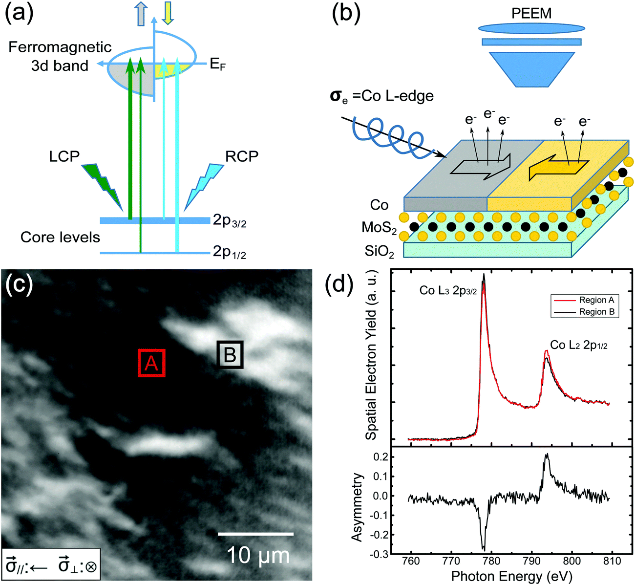 | ||
| Fig. 2 XMCD. (a) Schematic diagram describing the principle of XMCD. The excitations of spin-up and spin-down electrons from the 2p band are distinct when a circularly polarized beam is applied along with a particular magnetic domain. This absorption, and the resulting photoelectron emission, asymmetry is reversed with the beam focused on the domain in the opposite magnetization. (b) Schematic diagram illustrating the experimental setup. The incident circularly polarized soft X-ray beam has an angle of 25° with respect to the sample surface. Due to the effect of XMCD, opposite magnetic domains respond differently when the photon energy of the incident beam is resonant with the Co L3 and L2 edges. The emitted photoelectrons are collected with the PEEM to map spatially the domains in varied directions of magnetization. (c) XMCD image of cobalt (9 ML) on monolayer MoS2. The inset shows the direction of incident light. (d) The corresponding μ-XAS of regions A and B, the positions of which are marked in (c), are shown. The bottom spectrum represents the asymmetric nature of spectra A and B, which proves that the grey-scale contrast in (c) is a consequence of the XMCD effect. | ||
Fig. 3(a)–(c) show XMCD images of Co films at thicknesses 5, 7, and 9 ML. After recording the first XMCD image from a Co film at thickness 5 ML, the images in succeeding sets were acquired after each subsequent deposition. After comparing the series of images, we concluded that the additional Co deposition would only enhance the magnetic contrast of the existing domains. The XMCD image can be conceived as an inner product of the sample magnetization (![[M with combining right harpoon above (vector)]](https://www.rsc.org/images/entities/i_char_004d_20d1.gif) ) and the beam polarization (
) and the beam polarization (![[small sigma, Greek, vector]](https://www.rsc.org/images/entities/i_char_e1c9.gif) ), i.e. I ∝ ·.33 Under the conditions of fixed incident angle and beam polarization, the XMCD image is effectively a measure of the spatial distribution of magnetization directions with respect to the polarization of the photon beam. In our study, the thickness of Co was assumed to be uniform on MoS2,34,35 and likewise the magnitude of its magnetization. The fact that we observed only several distinct contrasts in Fig. 3 indicates that the localized magnetizations are somehow oriented into selected directions. To explain the directions of magnetization clearly, we plotted the contrast levels of domain images into histograms. The greyscale shown at the bottom of the histogram indicates the range of contrast levels taken from images, whereas the intensity of the histogram represents the frequency of finding a specific contrast level from the image pixels. In the hypothetical case of out-of-plane magnetization, only two contrast levels would be possible, inward-pointing normal and outward-pointing normal. As all histograms in Fig. 3 display more than two contrast levels within a finite greyscale, we conclude that the magnetizations of Co domains not only lie either in-plane or canted but also have preferred orientations.
), i.e. I ∝ ·.33 Under the conditions of fixed incident angle and beam polarization, the XMCD image is effectively a measure of the spatial distribution of magnetization directions with respect to the polarization of the photon beam. In our study, the thickness of Co was assumed to be uniform on MoS2,34,35 and likewise the magnitude of its magnetization. The fact that we observed only several distinct contrasts in Fig. 3 indicates that the localized magnetizations are somehow oriented into selected directions. To explain the directions of magnetization clearly, we plotted the contrast levels of domain images into histograms. The greyscale shown at the bottom of the histogram indicates the range of contrast levels taken from images, whereas the intensity of the histogram represents the frequency of finding a specific contrast level from the image pixels. In the hypothetical case of out-of-plane magnetization, only two contrast levels would be possible, inward-pointing normal and outward-pointing normal. As all histograms in Fig. 3 display more than two contrast levels within a finite greyscale, we conclude that the magnetizations of Co domains not only lie either in-plane or canted but also have preferred orientations.
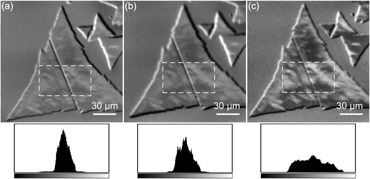 | ||
| Fig. 3 Dependence on the thickness of Co. XMCD images of Co of thicknesses (a) 5, (b) 7 and (c) 9 ML. The histograms below each image measure the grey-scale distribution in the region enclosed with the dashed squares in each histogram corresponding to the XMCD images. The domains in (a), (b) and (c) tend to be identical but the color contrast increases. The greyscale is limited to the range 0 to 255; the three chosen squares have the same area. The presence of several peaks in the histogram implies the magnetization to be in-plane. | ||
Our next task was to examine the relevance of the MoS2 crystalline structure for the domain formation. Fig. 4(a) and (b) display the domain images of a Co film (9 ML) grown on a single crystalline monolayer MoS2 flake and a polycrystalline monolayer MoS2 film, respectively.34 By controlling the degree of crystallinity in monolayer MoS2, we were able to adjust the lateral dimensions of the magnetic domains from tens of micrometers to sub-micrometers. In addition, as Fig. 4(b) shows a broader spread of greyscale, the Co domains on a polycrystalline surface are believed to be less aligned. Another observation worthy of mention concerns the domain boundaries on triangular MoS2 flakes. As displayed in Fig. 4(c), the paths of the domain boundary are not arbitrary but follow a particular crystalline axis of MoS2. Considering that CVD-grown triangular MoS2 flakes are typically treated as a single crystalline grain, and that the edge of the grain is in either an armchair or zig-zag configuration as illustrated in Fig. 4(d),36 it seems that well-defined crystallinity in the MoS2 layer would not only promote the magnetization alignment in a Co layer but also affect how the domains are divided. We emphasize here that the same behavior was found repeatedly on other flakes of MoS2 covered with Co.
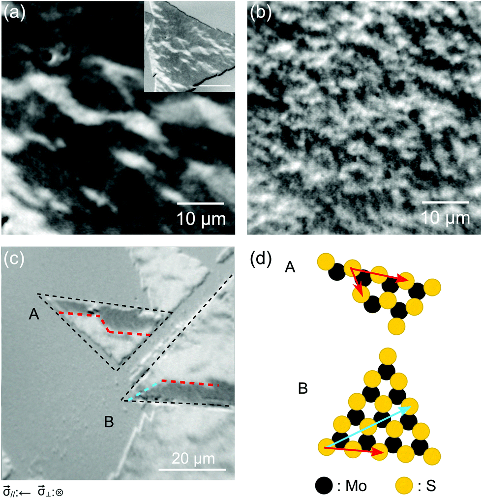 | ||
| Fig. 4 Magnetic anisotropy. XMCD images of (a) a Co film (9 ML) on a single grain monolayer MoS2 flake and (b) a Co film (9 ML) on polycrystalline monolayer MoS2. The inset in (a) shows a de-magnified image with a scale bar set at 30 μm. The domains are larger on single grain MoS2 than on polycrystalline MoS2 (c). The domain boundaries present preferential directions, parallel to either the zig-zag (red) or armchair (blue) direction as clearly seen in the corresponding MoS2 ball models, A and B, drawn in (d). | ||
Finally, we examined the electronic structure of Co/MoS2 (flake) with μ-XPS. Fig. 5 shows the μ-XPS recorded from the Co(4 ML)/SiO2 and the Co(4 ML)/MoS2 regions, respectively. As the Co layer was prepared in situ, under UHV conditions, the Co 2p core levels acquired in the two separate areas contain contributions mainly from Co(0) (2p3/2 = 778.3 eV),37 which corresponds to the metallic state of Co. Moreover, apart from a broad spectral feature corresponding to the Auger emission of S atoms in MoS2, there are noticeable differences between the two spectra displayed in Fig. 5. A fit of the Co 2p spectrum of Co/MoS2 (flake) produces two additional spectral features, namely Co(II) (2p3/2 = 781.5 eV) and Co(III) (2p3/2 = 779.7 eV).37,38 As Co(III) has an emission energy similar to that of Co oxidization found in Co/SiO2,39 we suggest that both Co(II) and Co(III) found on Co/MoS2 (flake) are the result of charge transfer from Co to MoS2. The spectra shown in Fig. 5 are inconsistent with the concept of chemical doping, which is generally accompanied by chemical shifts in XPS.40 Instead, the absence of an energy shift of all major emission peaks – Co(0), Mo 3d, and S 2p (Fig. S6, ESI†) – implies a small net extent of charge transfer.
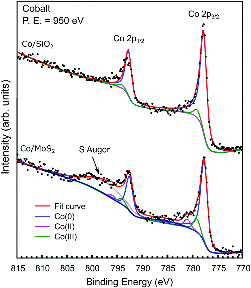 | ||
| Fig. 5 μ-XPS evidence of charge transfer in Co. Co 2p μ-XPS recorded for Co/SiO2 (upper) and Co/MoS2 (lower). | ||
Based on our experimental observations, we confirm that an ultrathin Co film deposited on monolayer MoS2 is able to form micrometer-sized ferromagnetic domains. Furthermore, the magnetization and the boundaries of domains have preferred directions or paths that are parallel to either the zig-zag or armchair directions of the MoS2 crystal structure. The presence of magnetic order and magnetic anisotropy in Co/MoS2 (flake) proves the possibility of using two-dimensional materials of monolayer thickness to evoke the anisotropy of a magnetic layer deposited thereon.
The crystal structure of Co offers the most straightforward explanation of the observed MA, because an ultrathin metallic film under a lattice strain can display properties different from those found in its pristine structure. An effective example to show what a lattice strain can do to the magnetic properties of a material is Co/GaAs(110); the Co layer stabilized on the body-center-cubic (BCC) structure displays an α-Fe-like behavior.41 However, as the low energy electron diffraction (LEED) results on Co/MoS2 (bulk crystal) failed to produce a sharp pattern, we suspect that Co/MoS2 (flake) might not be epitaxial in nature; in fact, the Co layer grown on the MoS2 surface seems amorphous (Fig. S7, ESI†). Although we lack the appropriate tool to determine the crystal structure of Co/MoS2 (flake), we know that the shape anisotropy can play no major role because of the non-comparable thickness between the Co layer and the area of the MoS2 flake (several nm vs. tens of μm2).
Readers might curious about the absence of magnetic domains in the part Co/SiO2. The uniformity of the Co layer could cause such a difference. However, with our Co deposition known to vary by at most a few percent within a diameter of 6 mm on the specimen and the confirmation of having the same Co L-edge intensity measured from Co/MoS2 and Co/SiO2 (Fig. S11, ESI†), we believe that the thickness of the Co layer is not responsible for the observed difference in domain configurations. Also, the AFM image (Fig. S12, ESI†) of a Pd protected Co film on the substrate shows that nanoclusters form on both MoS2 and SiO2. The absence of magnetic domains of Co/SiO2 means that the orientations of spin are in a high symmetry phase whose orientations have equal probabilities of pointing in every direction. This could be the reason why XMCD-PEEM cannot observe the magnetic domain, although Co is a ferromagnetic material. In contrast, the presence of magnetic domains is a signature of symmetry lowering in which spins are grouped and oriented into selected directions.
Regarding the XPS evidence of charge transfer from Co to MoS2, we find it consistent with the theoretical work of Garandel et al. that indicates that Co atoms at the interface bond covalently with the topmost S atoms of MoS2.26 According to that reported work,26 the charge transfer at Co/MoS2 would result in a spin-polarized metallic interface and facilitate efficient spin injection. Another reason motivating us to look into the electronic structures of Co/MoS2 and Co/SiO2 is the distinct behavior recently reported in Fe/MoS2 (Fig. S8 (ESI†), and ref. 24); neither magnetic domains nor charge transfer between Fe and MoS2 was found.
Conclusion
In conclusion, we have proved that a CVD-grown monolayer MoS2 flake can promote domain formation in a subsequently deposited Co layer. Furthermore, it is possible to fine-tune the magnetic behavior of Co/MoS2 through the crystallinity of MoS2. Finally, according to the XPS evidence of charge donation at Co/MoS2, we suggest that the orbital hybridization at the interface is what distinguishes the magnetic properties of Co/MoS2 here and Fe/MoS2 reported earlier.24,25 The interplay between Co and MoS2 is electronically originated, and such an interplay has resulted in a spontaneously induced magnetic anisotropy in an ultrathin Co/MoS2 heterojunction.Methods
High-quality single-crystal monolayer MoS2 flakes were grown inside a tubular furnace equipped with a silica tube (diameter 30 mm). SiO2 (90 nm)/Si(001) substrates were cleaned according to a standard procedure and then soaked in a H2SO4/H2O2 (3![[thin space (1/6-em)]](https://www.rsc.org/images/entities/char_2009.gif) :1) solution for 2 h. MoO3 powder (0.01 g) was then positioned on a silver silica boat located at the heating zone of the furnace. The SiO2/Si substrate (size 2 cm × 2 cm) was placed face down above the MoO3 powder. Sulfur powder was placed in a separate ceramic boat located at the upper stream of the furnace at a temperature of about 170 °C. A flow of ultrahigh-purity Ar gas carried both S and MoO3−x vapors onto the target substrate. The temperature of the furnace was initially raised to 120 °C (500 sccm) for 30 min, and then ramped up to 850 °C at a rate of 20 °C min−1 (200 sccm), allowing the CVD growth of MoS2. The sample was kept in the environment described above for a further 30 min before passive cooling to ∼25 °C.
:1) solution for 2 h. MoO3 powder (0.01 g) was then positioned on a silver silica boat located at the heating zone of the furnace. The SiO2/Si substrate (size 2 cm × 2 cm) was placed face down above the MoO3 powder. Sulfur powder was placed in a separate ceramic boat located at the upper stream of the furnace at a temperature of about 170 °C. A flow of ultrahigh-purity Ar gas carried both S and MoO3−x vapors onto the target substrate. The temperature of the furnace was initially raised to 120 °C (500 sccm) for 30 min, and then ramped up to 850 °C at a rate of 20 °C min−1 (200 sccm), allowing the CVD growth of MoS2. The sample was kept in the environment described above for a further 30 min before passive cooling to ∼25 °C.
The MoS2 samples grown on the SiO2(90 nm)/Si(001) substrates were loaded into TLS endstation 05B2 and heated at 150 °C for 6 h under ultra-high vacuum (UHV) conditions for outgassing. The Co layers were grown with a commercial EFM3; their thickness was defined in units of monolayer (ML). The rate of Co deposition was calibrated with the medium-energy electron-diffraction (MEED) oscillation recorded during the deposition of Co onto a Cu(001) single crystal. Note that it is necessary to check the structural stability of a 2D layer in a heterojunction. For that, we examine the micro-area XPS spectra taken from Co/MoS2/SiO2 (Fig. S6, ESI†). Compared to previous publications with ones acquired from CVD growth of MoS2, ref. 29, and Co-doped MoS2, ref. 40, the molybdenum Mo 3d and sulfur S 2p spectra reported in this work are in great resemblance to the ones acquired from a single layer of MoS2. We conclude that the chemical bond of monolayer MoS2 is preserved after Co deposition. Our argument above can be strengthened further by the nature of the strong covalent bonds within MoS2, whose melting point is 2375 °C. As the Co deposition (whose melting point is 1495 °C) is accomplished via an EFM3 evaporator at a slow deposition rate (## ML per minute), we believe the way we deposited Co is not likely to damage the atomic structure of MoS2.
After the Co deposition, the sample was transferred into the PEEM chamber27 under UHV conditions for XMCD imaging. We enhanced the domain images (or XMCD images) by the absorption asymmetry, IA = (IL3 − IL2)/(IL3 + IL2); that is, each XMCD image (IA) was actually an asymmetric superposition of two images, IL2 and IL3, recorded at L2 and L3, respectively. As this image processing can eliminate geometric inhomogeneity, the contrast in the IA image served to recognize the magnetic domains of varied magnetization directions.32,33 The exact magnetization direction of the domains could not be determined as it was not possible to rotate the sample in situ or to apply an external magnetic field in the PEEM experimental chamber. The system is hence sensitive only to whether the magnetic domains are parallel (brighter) or antiparallel (darker) with respect to the incident light. The XMCD images were leveled by subtracting the polynomial background, which is supposedly a consequence of a shift of the beam spot caused by a change in the photon energy. The micro-area X-ray absorption spectra (μ-XAS) recorded on A and B domains (displayed in Fig. 2(d)) were extracted from a stack of images recorded at a step of 0.2 eV from hν = 750 eV to 810 eV, across the Co L2,3 edges.
The μ-XPS measurements were performed at beamline 1.2L NanoESCA at the Elettra Synchrotron (Trieste, Italy).28 Before the deposition of cobalt, the MoS2/SiO2 samples were outgassed at 250 °C in a UHV preparation chamber for 2 h. Co 2p spectra were recorded using an s-polarized photon energy of 950 eV. Because of the decreased beam spot size on the sample (<20 μm) it was possible to record μ-XPS selectively from the Co/MoS2 flakes and Co/SiO2 regions.
Data availability
All relevant data are available from the authors. Requests for data and materials should be addressed to D.-H. Wei.Author contributions
C.-I. L. performed PEEM with assistance from C.-H. H. and T.-H. C. The data analysis was performed by C.-I. L. and discussed in depth with C. H. H., T.-H. C., Y.-W. L., and D.-H. W. The monolayer MoS2 flakes were grown by F. L., J. Q. and Y.-W. L. The polycrystalline monolayer MoS2 was grown by K.-S. L. μ-XPS were recorded by C.-I. L., K.-H., O. Y., M.-T. L, C.-H. H., M. J., I. C., V. F. and C. T. The project at the Elettra Synchrotron in Trieste (Italy) was proposed and conducted by T.-H. C. The manuscript was prepared by C.-I. L. and D.-H. W. with assistance from K. B. S., V. F. and Y.-W. L. This project was conceived and led by D.-H.W.Conflicts of interest
The authors declare no competing interests.Acknowledgements
We thank members of TLS 09A1 and TLS 09A2 for their suggestions on the analysis of XPS data and prior test measurements. We thank especially Dr Chia-Hao Chen, Dr Yao-Jane Hsu, Dr Hung-Wei Shiu, Dr Li-Chung Yu, Dr Shang-Hsien Hsieh and Dr Lo-Yueh Chang, and Dr Yao-Jui Chan at National Sun Yat-Sen University for the beamtime assistance. We also thank Dr Yu-Hsun Chu at National Taiwan University for fruitful discussion. Many thanks to Prof. Wen-Chin Lin and Chak-Ming Liu at National Taiwan Normal University (NTNU) for the Co thin film deposition, and thanks to Dr Rahul Kesarwani, a post doctoral researcher, also at NTNU, for the AFM characterization. This work was supported in part by Taiwan Ministry of Science and Technology through grants MOST 104-2112-M-213-002-MY3 (D.-H. Wei), MOST 105-2112-M-213-012-MY2 (T.-H. Chuang) and MOST 105-2112-M-003-016-MY3 (Y.-W. Lan). This work was also supported in part by National Nano Device Laboratories.References
- R. A. Bromley, R. B. Murray and A. D. Yoffe, The band structure of some transition metal dichalcogenides: III. Group VI A: trigonal prism materials, J. Phys. C: Solid State Phys., 1972, 5, 759–778 CrossRef CAS.
- L. F. Mattheiss, Band structure of transition-metal-dichalcogenide layer compounds, Phys. Rev. B: Solid State, 1973, 8, 3719–3740 CrossRef CAS.
- R. Coehoorn, et al., Electronic structure of MoSe2, MoS2, and WSe2. I. Band-structure calculations and photoelectron spectroscopy, Phys. Rev. B: Condens. Matter Mater. Phys., 1987, 35, 6195–6202 CrossRef CAS PubMed.
- A. K. Geim and I. V. Grigorieva, van der Waals heterostructures, Nature, 2013, 499, 419–425 CrossRef CAS PubMed.
- K. F. Mak, et al., Atomically thin MoS2: a new direct-gap semiconductor, Phys. Rev. Lett., 2010, 105, 136805 CrossRef PubMed.
- Y.-H. Lee, et al., Synthesis of large-area MoS2 atomic layers with chemical vapor deposition, Adv. Mater., 2012, 24, 2320–2325 CrossRef CAS PubMed.
- E. Cappelluti, et al., Tight-binding model and direct-gap/indirect-gap transition in single-layer and multilayer MoS2, Phys. Rev. B: Condens. Matter Mater. Phys., 2013, 88, 075409 CrossRef.
- W. Jin, et al., Direct measurement of the thickness-dependent electronic band structure of MoS2 using angle-resolved photoemission spectroscopy, Phys. Rev. Lett., 2013, 111, 106801 CrossRef PubMed.
- Q. H. Wang, et al., Electronics and optoelectronics of two-dimensional transition-metal dichalcogenides, Nat. Nanotechnol., 2012, 7, 699–712 CrossRef CAS PubMed.
- R. Cheng, et al., Electroluminescence and photocurrent generation from atomically sharp WSe2/MoS2 heterojunction p–n diodes, Nano Lett., 2014, 14, 5590–5597 CrossRef CAS PubMed.
- M. M. Furchi, et al., Device physics of van der Waals heterojunction solar cells, npj 2D Mater. Appl., 2018, 2, 3 CrossRef.
- Y. W. Lan, et al., Atomic-monolayer MoS2 band-to-band tunneling field-effect transistor, Small, 2016, 12, 5676–5683 CrossRef CAS PubMed.
- D. Xiao, et al., Coupled spin and valley physics in monolayers of MoS2 and other group-VI dichalcogenides, Phys. Rev. Lett., 2012, 108, 196802 CrossRef PubMed.
- X. Xu, W. Yao, D. Xiao and T. F. Heinz, Spin and pseudospins in layered transition metal dichalcogenides, Nat. Phys., 2014, 10, 343–350 Search PubMed.
- R. Roldán, et al., Momentum dependence of spin–orbit interaction effects in single-layer and multi-layer transition metal dichalcogenides, 2D Mater., 2014, 1, 034003 Search PubMed.
- K. F. Mak, K. He, J. Shan and T. F. Heinz, Control of valley polarization in monolayer MoS2 by optical helicity, Nat. Nanotechnol., 2012, 7, 494–498 CrossRef CAS.
- T. Cao, et al., Valley-selective circular dichroism of monolayer molybdenum disulphide, Nat. Commun., 2012, 3, 887 CrossRef PubMed.
- S. Wu, et al., Electrical tuning of valley magnetic moment through symmetry control in bilayer MoS2, Nat. Phys., 2013, 9, 149–153 Search PubMed.
- H. Zeng, et al., Valley polarization in MoS2 monolayers by optical pumping, Nat. Nanotechnol., 2012, 7, 490–493 CrossRef CAS PubMed.
- Z. Y. Zhu, Y. C. Cheng and U. Schwingenschlögl, Giant spin-orbit-induced spin splitting in two-dimensional transition-metal dichalcogenide semiconductors, Phys. Rev. B: Condens. Matter Mater. Phys., 2011, 84, 153402 CrossRef.
- H. Ochoa and R. Roldán, Spin-orbit-mediated spin relaxation in monolayer MoS2, Phys. Rev. B: Condens. Matter Mater. Phys., 2013, 87, 245421 CrossRef.
- W. Wang, et al., Spin-valve effect in NiFe/MoS2/NiFe junctions, Nano Lett., 2015, 15, 5261–5267 CrossRef CAS PubMed.
- K. Dolui, A. Narayan, I. Rungger and S. Sanvito, Efficient spin injection and giant magnetoresistance in Fe/MoS2/Fe junctions, Phys. Rev. B: Condens. Matter Mater. Phys., 2014, 90, 041401 CrossRef.
- H.-C. Hsu, et al., Surface morphology, magnetism and chemical state of Fe coverage on MoS2 substrate, Appl. Surf. Sci., 2015, 357, 551–557 CrossRef CAS.
- C.-C. Hsu, et al., Magnetic decoupling of Fe coverage across atomic step of MoS2 flakes on SiO2 surface., J. Phys. D: Appl. Phys., 2017, 50, 415001 CrossRef.
- T. Garandel, et al., Electronic structure of the Co(0001)/MoS2 interface and its possible use for electrical spin injection in a single MoS2 layer, Phys. Rev. B, 2017, 95, 075402 CrossRef.
- D.-H. Wei, Y.-L. Chan and Y.-J. Hsu, Exploring the magnetic and organic microstructures with photoemission electron microscope, J. Electron Spectrosc. Relat. Phenom., 2012, 185, 429–435 CrossRef CAS.
- C. M. Schneider, et al., Expanding the view into complex material systems: From micro-ARPES to nanoscale HAXPES, J. Electron Spectrosc. Relat. Phenom., 2012, 185, 330–339 CrossRef CAS.
- W. Park, et al., Photoelectron spectroscopic imaging and device applications of large-area patternable single-layer MoS2 synthesized by chemical vapor deposition, ACS Nano, 2014, 8, 4961–4968 CrossRef CAS PubMed.
- C.-T. Chen, F. Sette, Y. Ma and S. Modesti, Soft-x-ray magnetic circular dichroism at the L2,3 edges of nickel, Phys. Rev. B: Condens. Matter Mater. Phys., 1990, 42, 7262–7265 CrossRef CAS PubMed.
- J. L. Erskine and E. A. Stern, Calculation of the M23 magneto-optical absorption spectrum of ferromagnetic nickel, Phys. Rev. B: Solid State, 1975, 12, 5016–5024 CrossRef CAS.
- B.-Y. Wang, et al., Flipping magnetization induced by noncollinear ferromagnetic-antiferromagnetic exchange coupling, Phys. Rev. B: Condens. Matter Mater. Phys., 2012, 85, 094412 CrossRef.
- J. Stöhr and H. Siegmann, Magnetism: From fundamentals to nanoscale dynamics. Berlin Germany, Springer, 2006 Search PubMed.
- Please refer to the ESI,† online for further detailed discussion.
- Q. Chen, et al., Uniformly wetting deposition of Co atoms on MoS2 monolayer: a promising two-dimensional robust half-metallic ferromagnet, ACS Appl. Mater. Interfaces, 2014, 6, 16835–16840 CrossRef CAS PubMed.
- C.-I. Lu, et al., Graphite edge controlled registration of monolayer MoS2 crystal orientation, Appl. Phys. Lett., 2015, 106, 181904 CrossRef.
- NIST X-ray Photoelectron Spectroscopy Database, Version 4.1, National Institute of Standards and Technology, Gaithersburg USA, 2012, http://srdata.nist.gov/xps/ Search PubMed.
- Y. Chen, S. Zhao and Z. Liu, Influence of the synergistic effect between Co-N-C and ceria on the catalytic performance for selective oxidation of ethylbenzene, Phys. Chem. Chem. Phys., 2015, 17, 14012–14020 RSC.
- S. Entani, M. Kiguchi, S. Ikeda and K. Saiki, Magnetic properties of ultrathin cobalt films on SiO2 substrates, Thin Solid Films, 2005, 493, 221–225 CrossRef CAS.
- J. Ye, et al., Synthesis of Co-doped MoS2/graphene hybrids as enhanced electrocatalysts for the hydrogen evolution reaction, RSC Adv., 2016, 6, 104925–104932 RSC.
- G. A. Prinz, Stabilization of bcc Co via epitaxial growth on GaAs, Phys. Rev. Lett., 1985, 54, 1051–1054 CrossRef CAS PubMed.
Footnote |
| † Electronic supplementary information (ESI) available. See DOI: 10.1039/d0nh00108b |
| This journal is © The Royal Society of Chemistry 2020 |