
 Open Access Article
 This Open Access Article is licensed under a Creative Commons Attribution-Non Commercial 3.0 Unported Licence
Interface engineering strategies towards Cs2AgBiBr6 single-crystalline photodetectors with good Ohmic contact behaviours†
Yangyang
Dang
,
Guoqing
Tong
,
Wentao
Song
,
Zonghao
Liu
,
Longbin
Qiu
 ,
Luis K.
Ono
and
Yabing
Qi
*
,
Luis K.
Ono
and
Yabing
Qi
*
Energy Materials and Surface Sciences Unit (EMSSU), Okinawa Institute of Science and Technology Graduate University (OIST), 1919-1 Tancha, Onna-son, Kunigami-gun, Okinawa 904-0495, Japan. E-mail: Yabing.Qi@OIST.jp
First published on 19th November 2019
Abstract
Lead-free double perovskite materials have attracted much interest for optoelectronic applications due to their nontoxicity and high stability. In this work, centimetre-sized Cs2AgBiBr6 single crystals were successfully grown using methylammonium bromide (MABr) as the flux by a top-seeded solution growth (TSSG) method. The low-temperature crystal structure of Cs2AgBiBr6 single crystals was determined and refined. To investigate the interface problems between Cs2AgBiBr6 single crystals and electrodes, the optical band gap, X-ray photoelectron spectroscopy (XPS), and ultraviolet photoemission spectroscopy (UPS) measurements were performed on Cs2AgBiBr6 single crystals. More importantly, we investigated the photodetectors based on Cs2AgBiBr6 single crystals with different contact electrodes (Au, Ag, and Al). It is found that a good Ohmic contact with Ag electrodes enables excellent photo-response behaviors. Furthermore, we studied the photodetectors based on Cs2AgBiBr6 single crystals using Ag electrodes under room and low temperature conditions, which underwent phase transition. Cs2AgBiBr6 single crystal photodetectors show clear differences at room and low temperatures, which is caused by the work function changes of Cs2AgBiBr6 single crystals induced by the reversible phase transition. These attractive properties may enable opportunities to apply emerging double perovskite single-crystalline materials for high-performance optoelectronic devices.
Introduction
Lead (Pb)-based hybrid perovskite materials have attracted tremendous attention owing to their outstanding properties when applied in photovoltaic devices.1,2 Power conversion efficiencies (PCEs) as high as 25.2% have been achieved for Pb-based perovskite solar cells.3 However, the toxicity and instability of Pb-based perovskite materials need to be solved. It is imperative to search for alternative perovskite materials containing only non-toxic elements. A strategy is to replace the toxic Pb2+ with two different oxidation states Ag+ and Bi3+ to form double perovskite materials.4 Several nontoxic candidates such as Cs2AgBiX6 (X = Cl, Br),5 (CH3NH3)2AgBiBr66 and so on have been reported. In particular, Cs2AgBiBr6 is considered to be an appealing lead-free semiconducting material due to its promising optoelectronic properties.7 Woodward and coworkers reported the solid-state synthesis and the crystal structure of Cs2AgBiX6 (X = Cl, Br) with the cubic system with Fm![[3 with combining macron]](https://www.rsc.org/images/entities/char_0033_0304.gif) m (no. 225) by powder X-ray diffraction (PXRD) experiments and Rietveld refinements.5 The computational design and the experimental synthesis of Pb-free halide double perovskites including the band gaps and stability of Cs2AgBiX6 (X = Cl, Br) were reported by Giustino and coworkers.8–10 Band structure calculations of Cs2AgBiBr6 perovskite based on the order–disorder transition by a first principles study were performed in detail by Wei and coworkers.11 Structural analysis and optical properties of Cs2AgBiBr6 powder samples below and above the phase transition point were introduced by Schade and coworkers.12 The authors reported the low-temperature and room-temperature crystal structure parameters on the basis of neutron powder diffraction (NPD), but they did not obtain the single-crystal structure.12 Zhan and coworkers investigated the application of Cs2AgBiBr6 thin films as humidity sensors, which exhibited superfast recovery times as well as high stability.13 In many cases, optoelectronic devices, such as solar cells14,15 and X-ray detectors,16 based on double perovskites are in the form of pressed powder (pellets) and thin films.
m (no. 225) by powder X-ray diffraction (PXRD) experiments and Rietveld refinements.5 The computational design and the experimental synthesis of Pb-free halide double perovskites including the band gaps and stability of Cs2AgBiX6 (X = Cl, Br) were reported by Giustino and coworkers.8–10 Band structure calculations of Cs2AgBiBr6 perovskite based on the order–disorder transition by a first principles study were performed in detail by Wei and coworkers.11 Structural analysis and optical properties of Cs2AgBiBr6 powder samples below and above the phase transition point were introduced by Schade and coworkers.12 The authors reported the low-temperature and room-temperature crystal structure parameters on the basis of neutron powder diffraction (NPD), but they did not obtain the single-crystal structure.12 Zhan and coworkers investigated the application of Cs2AgBiBr6 thin films as humidity sensors, which exhibited superfast recovery times as well as high stability.13 In many cases, optoelectronic devices, such as solar cells14,15 and X-ray detectors,16 based on double perovskites are in the form of pressed powder (pellets) and thin films.
Single crystals with the absence of grain boundaries and low densities of traps provide an ideal test platform for fundamental studies on the properties of double perovskites. For example, in a study employing a single crystal CH3NH3PbI3 perovskite sample (thickness = 20 μm), an outstanding PCE of 21.09% and a fill factor (FF) of up to 84.3% were reported.17 Therefore, it will be interesting to employ Cs2AgBiBr6 double perovskite single crystals in optoelectronic applications, but currently such studies are still scarce. In 2016, Karunadasa and coworkers reported for the first time that the room-temperature crystal structure and fundamental optical properties of Cs2AgBiBr6 single crystals were obtained by the temperature-cooling method.18 Tang and coworkers reported X-ray detectors based on Cs2AgBiBr6 single crystals, which exhibited a low detection limit.19 Roeffaers and coworkers studied the photophysical properties of Cs2AgBiBr6 single-crystalline X-ray detectors influenced by the carrier dynamics at both room- and liquid nitrogen-temperatures.20 Recently, Gao and coworkers have studied the reversible thermochromism and device fabrication of Cs2AgBiBr6 based on both single crystals and thin films.21 Meanwhile, Fan et al. observed the regulation of the order–disorder phase transformations in Cs2AgBiBr6 single crystals in an X-ray detector by the addition of phenylethylamine bromide (PEABr), which exhibited obvious ordered arrangements.22 In these studies, however, hysteresis phenomena in the I–V curves were evident in Cs2AgBiBr6 single crystal X-ray detectors based on gold (Au) electrodes.19,20,22 Zhang and coworkers reported the optical and electrical properties of Cs2AgBiBr6 double perovskite single crystals.23 To date, there have been no reports on the interfaces between Cs2AgBiBr6 single crystals and electrodes in their photodetectors.
In this work, centimeter-sized Cs2AgBiBr6 single crystals were successfully grown using MABr as the flux in the mother solution by the TSSG method. The structure of Cs2AgBiBr6 single crystals below the phase transition point was systematically studied. To investigate the interface relationships between Cs2AgBiBr6 single crystals and electrodes the band gap, X-ray photoelectron spectroscopy (XPS) and ultraviolet photoemission spectroscopy (UPS) measurements were performed on Cs2AgBiBr6 single crystals. More importantly, we investigated the photodetectors based on Cs2AgBiBr6 single crystals with different electrodes of gold (Au), silver (Ag), and aluminum (Al) at different wavelengths both in ambient air (relative humidity = 20%) and under vacuum. It is demonstrated that Cs2AgBiBr6 single crystal-based photodetectors using Ag electrodes exhibit better Ohmic contact behaviors than Au and Al. We also performed a systematic study on Cs2AgBiBr6 single crystal-based photodetectors using Ag electrodes at room and low temperatures, and the other two cases showed clear differences in photo-response and hysteresis. These properties may enable new opportunities to apply these emerging double perovskite single crystalline materials in high performance optoelectronic devices.
Results and discussion
Bulk Cs2AgBiBr6 single crystals with dimensions of 10 mm × 9 mm × 6 mm (Fig. 1a) were grown using MABr as the flux in the HBr–H3PO2 mixed solution in an ambient atmosphere, according to previous crystal growth methods.24–27 The theoretical morphology deduced by the Bravais–Friedel–Donnay–Harker (BFDH) method28 is shown in Fig. 1b. The theoretical crystal facets are determined to be (200) and (111). The single crystal growth requires suitable solubility, flux, saturation, and temperature control. We used the seed crystal growth method to select the seed crystal direction to control the shape and size. Thus, we could obtain controllable shape and size, which led to good device reproducibility. It is easier to obtain large size Cs2AgBiBr6 single crystals with MABr as the flux as shown in Fig. S1 (ESI†), because MABr can increase the solubility for Cs2AgBiBr6 single crystal growth owing to the enhanced dissolution of Cs2AgBiBr6 materials induced by MABr. Cs2AgBiBr6 single crystals were grown in saturated perovskite precursor solutions. Meanwhile, the crystal structure of Cs2AgBiBr6 at room temperature (Fig. 1c and Table S1, ESI†) was determined and refined with the formula Cs4Ag2Bi2Br12, which exhibited the cubic space group of Fmm (no. 225) consistent with a previous report.18 Based on a previous report on the crystal structure under phase transition from the powder sample,12 we carried out the low-temperature crystal structure measurements. The crystal structure determinations and refinements at 100 K by single-crystal X-ray diffraction analysis demonstrated that there were two possibilities for the pseudopolymorphic phase, i.e., tetragonal or cubic space groups (Table S1, ESI†). Based on a previous report,12 Cs2AgBiBr6 single crystals undergo a reversible phase transition (Fig. S2 and Table S1, ESI†). The related crystal parameters are listed in Table S1 in the ESI.† It is demonstrated that a Cs2AgBiBr6 single crystal at 100 K exhibits the tetragonal space group I4/m (no. 87), which is consistent with the report of Schade et al.12 Based on the single crystal determination, we did not observe MA cations in the low temperature crystal structure. Therefore, it is verified that there exists no MABr in Cs2AgBiBr6 single crystals. Moreover, in Fig. 1d we did not observe redundant peaks for MABr. Besides, the N 1s peak was not observed according to XPS in Fig. S3 (ESI†). The PXRD pattern agrees well with the simulated XRD pattern of Cs2AgBiBr6 single crystals, as shown in Fig. 1d.
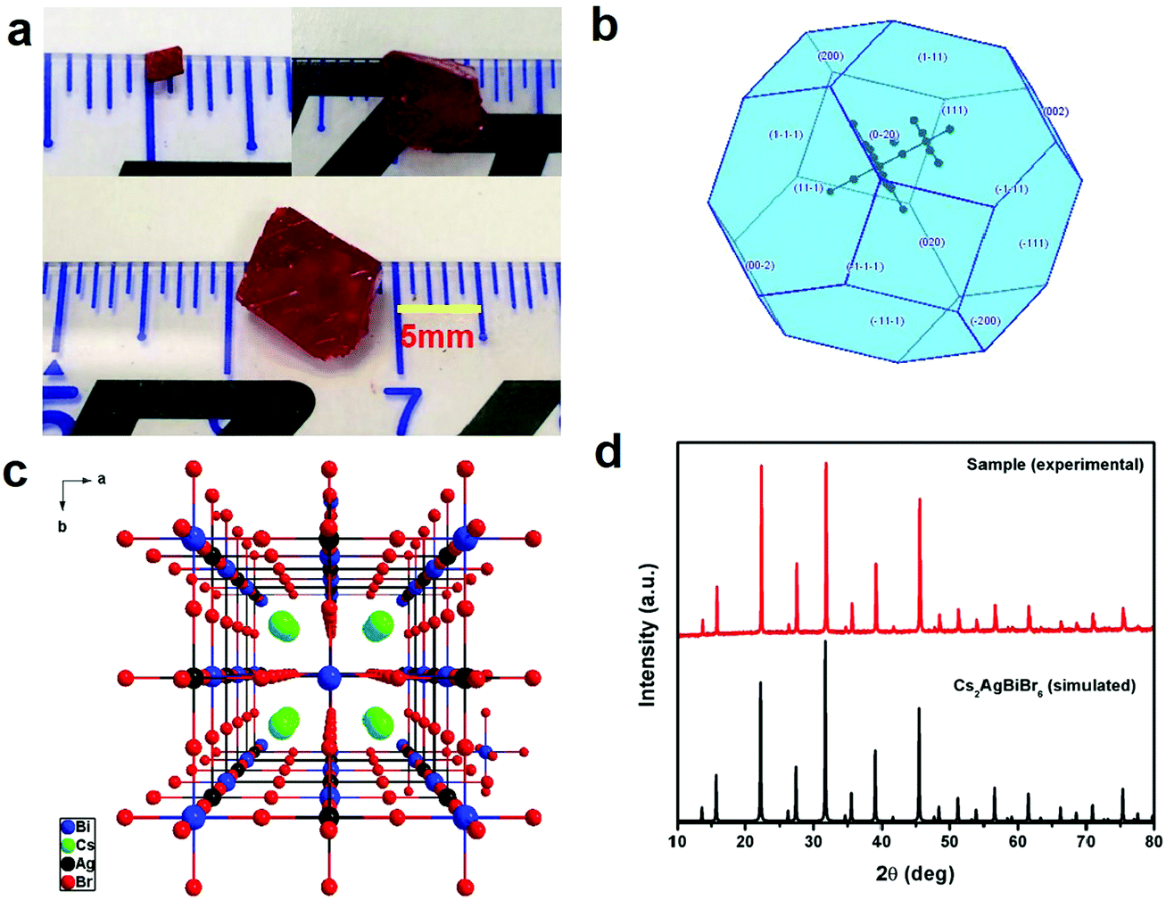 | ||
| Fig. 1 (a) Photos of a Cs2AgBiBr6 single crystal; (b) theoretical morphology of the Cs2AgBiBr6 single crystal deduced by the Bravais–Friedel–Donnay–Harker (BFDH) method;28 (c) crystal structure of Cs2AgBiBr6 at room temperature; and (d) comparison between the experimental and simulated X-ray diffraction patterns of Cs2AgBiBr6. | ||
XPS was employed to further determine the elemental composition of Cs2AgBiBr6 double perovskites.29–31 Although Cs2AgBiBr6 single crystals are stable in ambient atmosphere, to avoid the influence of oxygen and humidity, the surface of each single crystal was first cleaved by a sharp knife in an Ar atmosphere and then polished by abrasive paper and silk textile (Fig. 2a and Fig. S3, S4, ESI†). The XPS survey in Fig. S3a (ESI†) reveals that these single crystal samples have high percentage of atomic concentrations of Cs, Ag, Bi and Br, and the amount of C and O is negligible. The high-resolution XPS spectra of Cs 3d, Ag 3d, Bi 4f, and Br 3d core levels are shown in Fig. S3c–f (ESI†). The peaks at binding energies of 724.6 eV and 738.6 eV are attributed to the Cs 3d5/2 and 3d3/2 core levels (Fig. S3c, ESI†), respectively. The peaks located at binding energies of 368.1 eV and 374.1 eV are attributed to the Ag 3d5/2 and 3d3/2 core levels (Fig. S3d, ESI†), respectively. The peaks located at binding energies of 159.2 eV and 164.6 eV are attributed to Bi 4f7/2 and 4f5/2 core levels (Fig. S3e, ESI†), respectively. The peaks located at binding energies of 68.5 eV and 69.5 eV are attributed to the Br 3d5/2 and 3d3/2 core levels (Fig. S3f, ESI†), respectively. These results are consistent with a previous report on Cs2AgBiBr6 thin films.29 To determine the detailed electronic structure, we performed UPS measurements on the single crystal samples to determine the work function (WF) and valence band maximum (VBM). The UPS survey based on the Cs2AgBiBr6 single crystals is shown in Fig. 2c. Based on the secondary electron onset of the UPS spectrum (Fig. 2c), the WF value of Cs2AgBiBr6 single crystals is determined to be 4.28 eV, which is smaller than that (5.01 eV) of the Cs2AgBiBr6 thin film samples.29 Similarly, in previous reports, the WF value of MAPbBr3 single crystals was determined to be 4.61 eV,32 while the WF value of MAPbBr3 thin films was determined to be 5.12 eV.33 The ionization energy is defined as the energy difference between the vacuum level and VBM. Kahn and coworkers proposed the determination of VBM onsets in perovskites to be conducted in semi-log plots.34,35 Accordingly, the ionization energy value is determined to be 5.64 eV (Fig. 2c and d), which is smaller than the previously reported value based on the Cs2AgBiBr6 thin films (7.13 eV).29 The differences are possibly caused by the following reasons: (1) different preparation methods can have an influence on the perovskite energy levels36a and (2) single crystals exhibit no grain boundaries and low densities of traps, while polycrystalline thin films have grain boundaries and high densities of electronic traps.36b Combined with the optical band gap (2.0 eV) from Fig. 2b, the conduction band minimum (CBM) is deduced to be at a position of 3.64 eV below the vacuum level in Fig. 2d. It seems that the WF of Cs2AgBiBr6 single crystals theoretically matches well with that of the electrodes in the order of Al > Ag > Au according to their energy levels.
 | ||
| Fig. 2 (a) Photo of the Cs2AgBiBr6 single crystal measured by XPS and UPS; (b) optical band gap of the Cs2AgBiBr6 material; (c) UPS of the Cs2AgBiBr6 single crystal; inset: semi-log scale analysis of Fermi-level versus VBM position, and (d) the energy level diagram of the Cs2AgBiBr6 single crystal and different electrodes (Au, Ag and Al). | ||
The quality of the Cs2AgBiBr6 single crystals is verified by evaluating the trap state density, mobility and PL decay lifetime (Fig. S5 and S6, ESI†). The obtained high-quality Cs2AgBiBr6 single crystals were cleaved and polished by mechanical processing (Fig. S4, ESI†) before incorporating into a Au/Cs2AgBiBr6 thin single crystal/Au vertical device as shown in Fig. S5 (ESI†). The trap state density (ntrap) in the Cs2AgBiBr6 single crystals was determined by the dark current–voltage (I–V) measurement and analyzing the trap filled limit voltage (VTFL), as shown in Fig. S5a (ESI†). It is found that there exist three regions in the dark J–V curve. With the increase of the applied voltage V, the current increases linearly, which shows the Ohmic behavior (n = 1) between the Au electrode and the perovskite when the applied voltage is lower than the first inflection point at (V = 3.48 eV).35 A further increase in the applied voltage leads to a fast-nonlinear rise (n > 3) in the current. The first inflection point voltage is associated with the trap filling process, and the trap state density and carrier mobility can be computed according to eqn (1) and (2)37
 | (1) |
 | (2) |
To obtain high-performance optoelectronic devices, it is important to clarify the impact of the interface between Cs2AgBiBr6 single crystals and electrodes. Insertion of interface layers between perovskite crystals and top electrodes has been demonstrated to attain Ohmic contacts by suitable energy matching.15,17 For example, Wu and coworkers employed P3HT between the perovskite crystal Cs2AgBiBr6 and Au electrode.15 On the other hand, the search for a viable electrode leading to a good Ohmic contact in Cs2AgBiBr6 single-crystal photodetectors is also advantageous considering the simplicity of the device structure. We first investigate the crystal/electrode interface of the Cs2AgBiBr6 single crystal photodetectors equipped with different electrodes under illumination at different wavelengths at room temperature in air and vacuum atmospheres. Fig. 3 and Fig. S7 (ESI†) illustrate the photodetectors based on the Cs2AgBiBr6 single crystals coated with different electrodes (Au, Ag, and Al), with an electrode area of 1 mm2 in length and width, channel = 50 μm, and thickness ≈ 80 nm. For photodetector measurements, a solar simulator is used as the light source and the power density is close to 66.3 mW cm−2. The influence of oxygen and humidity on Cs2AgBiBr6 single crystalline photodetectors was investigated employing a probe station that allows vacuum pumping and a controlled atmosphere. We investigated the differences in photo-responses of Cs2AgBiBr6 single crystal photodetectors with different electrodes in air and under vacuum conditions. Fig. 3 and Fig. S7 (ESI†) show the I–V curves and photo-responses in air with the light turned on and off for several cycles. In addition, the photodetectors based on Au and Al electrodes under vacuum exhibited current hysteresis phenomena, which is consistent with previous reports based on Au electrodes.19,20,22 It is concluded that oxygen and H2O may reduce current hysteresis phenomena. The work function of the Cs2AgBiBr6 single crystal theoretically matches well with that of Al electrodes (Fig. 2d). However, Al tends to react with the Cs2AgBiBr6 single crystal, which leads to poor photodetector performance and a hysteresis phenomenon. Similarly, Ahmad and coworkers investigated the interfacial properties of Al and Ag contacts on MAPbBr3 single crystals, and also found that Al easily reacted with MAPbBr3 perovskite crystals.38 Interestingly, Cs2AgBiBr6 single crystal-based photodetectors using Ag electrodes exhibited excellent photo-response behaviours both in air and under vacuum. In Table S2 (ESI†), the calculated responsivity of Cs2AgBiBr6 single crystal devices in air and under vacuum at 293 K is 0.9 and 0.92 mA W−1 for the device under 400 nm illumination with a bias of 5 V, respectively. In addition, we assume that the dark current is dominated by the shot noise for estimating detectivity (D*) (ESI,† eqn (S2)).46c The corresponding D* of the device is calculated to be 1.38 × 10⁹ and 2.66 × 10⁹ Jones (Jones = cm Hz1/2 W−1), respectively.46 The ON/OFF ratio of the device in air and under vacuum at 293 K is 42 and 153 at a bias of 5 V, respectively, which exhibits better performance than thin film-based photodetectors previously reported by He and coworkers.29 Compared with Au and Al electrodes (Fig. S7d and h, ESI†), Cs2AgBiBr6 single crystal photodetectors using a Ag electrode exhibit stable photo-response under vacuum at 293 K (Fig. 3b and d). This observation is attributed to the excellent Ohmic contact of Ag with the Cs2AgBiBr6 single crystal.
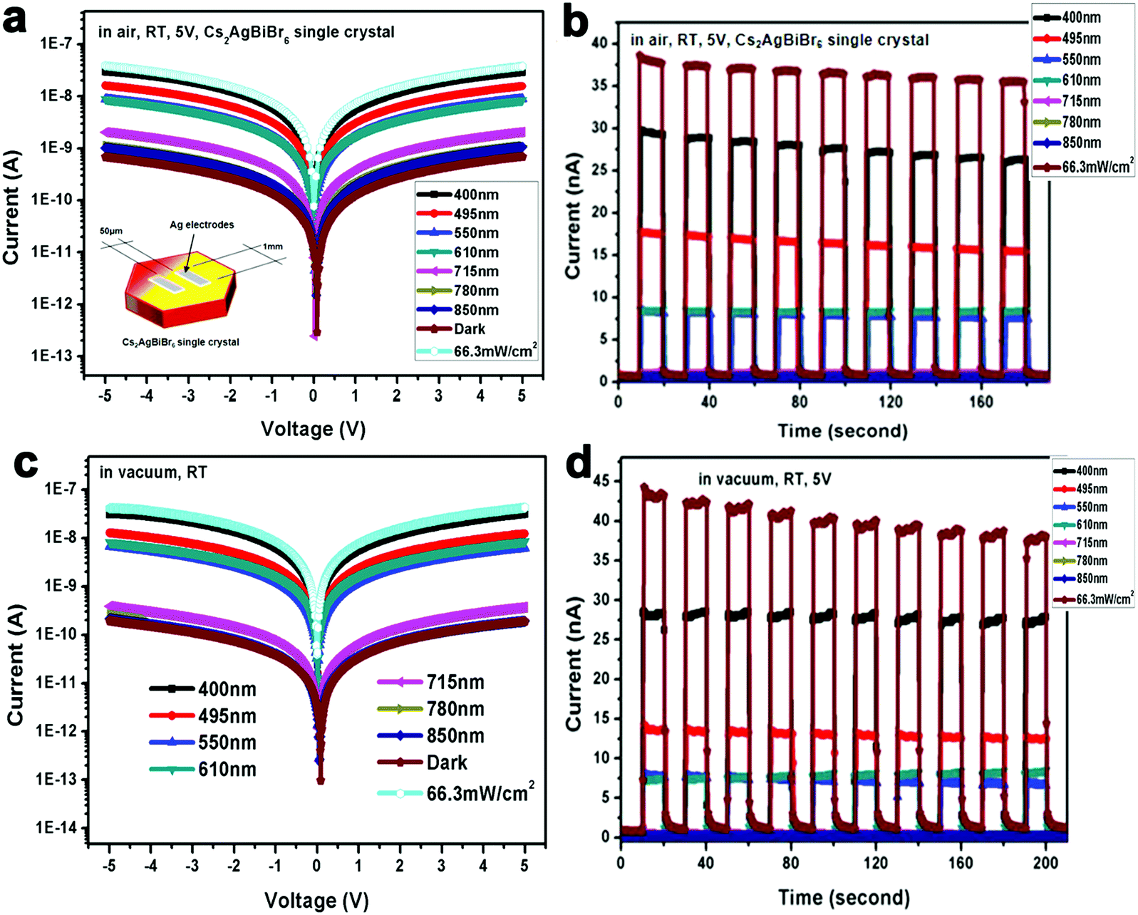 | ||
| Fig. 3 Comparisons of Cs2AgBiBr6 single-crystalline photodetector behaviours based on Ag electrodes at different wavelength under air and vacuum conditions. (a–d) Photodetector data (I–V and I–time curves) of Cs2AgBiBr6 single crystals based on Ag electrodes at bias voltage (5 V) when measured (a and b) in air with a relative humidity of 20% and (c and d) under vacuum (P = 3 × 10⁻⁷ Torr). All the measurements are performed at room temperature conditions. | ||
We propose that the superior Ohmic contact of Ag and the Cs2AgBiBr6 single crystal versus Al and Au is due to the strong interaction of Ag and Cs2AgBiBr6. There are two possible explanations about Ohmic contact using Ag electrodes: (1) in Fig. 1c, it is observed that every [AgBr6]5−/[BiBr6]3− octahedron in the crystal structure of Cs2AgBiBr6 is surrounded by six [BiBr6]3−/[AgBr6]5− octahedra, because there exist evident differences between the charges of Ag+ and Bi3+ cations to form a different coordination environment in the crystal structure. Thus, Cs2AgBiBr6 exhibits a disordered crystal structure at room temperature, which is consistent with previous reports.22,39 Based on the lattice-matching theory and size effect of ionic radius,40 Ag atoms can easily permeate into the Cs2AgBiBr6 single crystals and balance the charge leading to a better Ohmic contact of the Ag electrode than Au and Al electrodes. (2) Cs2AgBiBr6 exhibited the n-type semiconductor properties. According to the energy band bending theory, when the metal work function is smaller than that of the semiconductors, as shown in Fig. S8 (ESI†), there exists no Schottky barrier and the metal–semiconductor contact using Ag electrodes is Ohmic, and vice versa based on the devices using Au electrodes in Fig. S8 (ESI†).41,42 Therefore, Cs2AgBiBr6 single crystals exhibit superior Ohmic contact, which can effectively reduce the contact barrier, which helps promote charge carrier transport. It is demonstrated that the electron barrier transports from Ag electrodes to Cs2AgBiBr6 perovskite single crystals in the dark to illustrate that the WF of Ag electrodes minus the Cs2AgBiBr6 electron affinity helps form the good Ohmic contact. The response time is a key parameter to evaluate the performance of photodetectors. The rise time (trise) and fall time (tfall) are defined as the increase from 10% to 90% of the maximum value and decrease from 90% to 10% of the maximum value, respectively, in Fig. S9 (ESI†). The corresponding rise/fall times of Cs2AgBiBr6 single crystal photodetectors in air and under vacuum are 159/85 ms and 75/38 ms, respectively, which are better than those of the Cs2AgBiBr6 thin film as seen in Table S3 (ESI†). Besides, based on the above energy level and experimental result analysis of electrodes, we observe the dark current decrease of Cs2AgBiBr6 single crystal devices based on different wavelengths from Au, Ag and Al in this order in air and vacuum atmospheres at 293 K in Fig. 3 and Fig. S7 (ESI†). Cs2AgBiBr6 single crystal devices using Au and Al exhibit an obvious hysteresis with an increase in photocurrent like memristor behaviors.43 The photocurrent reduced quicker under vacuum than in air. The possible reason for the photocurrent to reduce more quickly under vacuum than in air is that oxygen and H2O in air affect the surface of the double perovskite device and have an impact on the photocurrent, compared with the vacuum case.47,48 We also measured the stability of Cs2AgBiBr6 single crystal photodetectors in air and vacuum atmospheres when exposed to 400 nm light irradiation condition. Cs2AgBiBr6 single crystal photodetectors showed relatively good stability in Fig. S10 (ESI†). These intriguing results can provide guidance for obtaining high performance lead-free perovskite Cs2AgBiBr6 single crystal optoelectronic devices.
Finally, we investigate the Cs2AgBiBr6 single crystal photodetector performance at low temperature. Based on a previous report on the phase transition of Cs2AgBiBr6 materials,12 we found that our Cs2AgBiBr6 single crystals also undergo phase transition. As shown in Fig. S2 (ESI†), Cs2AgBiBr6 single crystals exhibited two different crystal structures above and below the phase transition point (293 K and 100 K), which was consistent with the results previously reported by Schade and coworkers.12 To investigate the Ohmic contact behaviors at the Cs2AgBiBr6/Ag interfaces below and above the phase transition point, we carried out the Cs2AgBiBr6 single crystal photodetector measurement using Ag electrodes in a vacuum atmosphere at 293 K and 100 K. We carried out the photodetector measurements in a vacuum atmosphere at 100 K at different applied voltages with a solar simulator (power intensity of 66.3 mW cm−2) and at different wavelengths, as shown in Fig. 4 and Fig. S11 (ESI†). It was found that Cs2AgBiBr6 single crystals did not exhibit Ohmic contact behaviors at a low temperature of 100 K, as shown in Fig. 4 and Fig. S11 (ESI†). This observation is different from the above studies at room temperature under vacuum in Fig. 3. In particular, with the light turned on and off for several cycles using different wavelengths, the dark current of Cs2AgBiBr6 single crystals was shifted. The formation of a poor Ohmic contact for Cs2AgBiBr6/Ag photodetectors at low temperature is possibly caused by the changes in crystal structure arrangements induced by the temperature-dependent phase transition.44 Therefore, high-performance optoelectronic devices with good Ohmic contact can be achieved based on the suitable temperature and suitable electrodes for perovskite single crystal materials.
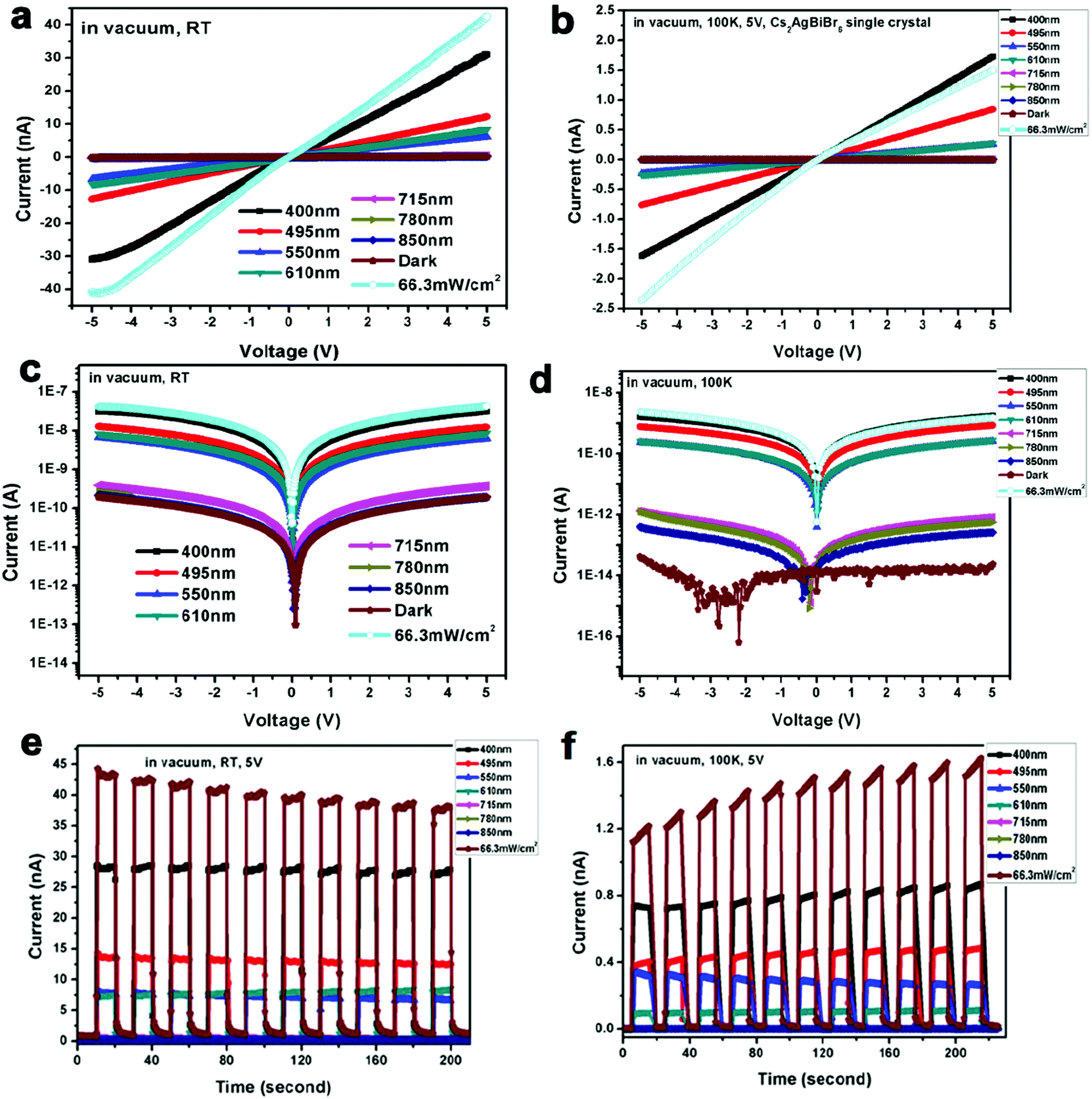 | ||
| Fig. 4 Comparisons of Cs2AgBiBr6 single-crystalline photodetector behaviors based on Ag electrodes at different wavelengths at room and low temperature. (a, c and e) Photodetector data (I–V and I–time curves) of Cs2AgBiBr6 single crystals based on Ag electrodes at different wavelengths at room temperature; (b, d and f) photodetector data (I–V and I–time curves) of Cs2AgBiBr6 single crystals based on Ag electrodes at different wavelengths at 100 K. All the measurements are performed under vacuum conditions (P = 3 × 10⁻⁷ Torr). | ||
Conclusions
In summary, we obtained large-size Cs2AgBiBr6 double perovskite single crystals by means of the addition of MABr as the flux. The optical band gap, XPS and UPS measurements were performed on Cs2AgBiBr6 single crystals. Photodetectors based on Cs2AgBiBr6 single crystals with different electrodes Au, Ag, and Al under a light source with different wavelength filters were studied. In addition, there is the influence of environment (air and vacuum atmospheres) as well as temperature (293 K and 100 K). It is concluded that photodetectors based on Cs2AgBiBr6 single crystals exhibit excellent photo-response by achieving Ohmic contact with Ag electrodes. In addition, photodetectors based on Cs2AgBiBr6 single crystals with Ag electrodes under room and low temperature conditions under which phase transition occurred were also systematically investigated. We believe that the present work not only provides an effective way to understand the intrinsic properties of Cs2AgBiBr6 single crystals, but also paves the way for high-performance Cs2AgBiBr6 single crystal photodetectors.Experimental
Reagents
All starting reagents including Cs2CO3 (97%, Wako), Ag2CO3 (99%, Sigma-Aldrich), (BiO)2CO3 (80–82.5% Bi basis, Sigma-Aldrich), methylammonium bromide (99%, Dyesol), HBr (48%, Sigma-Aldrich) and H3PO2 (50 wt% in H2O, Sigma-Aldrich) solutions were used without further purifications.Synthesis and crystal growth
The precursor synthesis of Cs2CO3, Ag2CO3 and (BiO)2CO3 in HBr and H3PO2 mixed solution was performed according to the chemical stoichiometric ratios. Cs2CO3 (6.5100 g, 0.020 mol), Ag2CO3 (2.7500 g, 0.010 mol), (BiO)2CO3 (5.0997 g, 0.010 mol) and MABr (2.2400 g, 0.02 mol) were dissolved in 200 ml HI and 20 ml H3PO2 mixed solution at 80 °C under constant stirring, forming a yellow transparent solution after three days. Solutions were saturated at 75 °C. Large size Cs2AgBiBr6 single crystals were grown by a temperature-lowering method using a top-seeded solution growth (TSSG) method in an ambient atmosphere for about two weeks, as shown in Fig. 1a.XPS and UPS measurements of Cs2AgBiBr6 single crystals
Cs2AgBiBr6 single crystals were cleaved and then fixed to the sample holders, as shown in Fig. 2a. The UPS and XPS spectra were measured on an X-ray photoelectron spectrometer (XPS-AXIS Ultra HAS, Kratos) equipped with monochromatic Al-Kα (1486.6 eV) and nonmonochromatic He-I (21.22 eV) sources, respectively. All the measurements were carried out in a vacuum atmosphere (<10−5 Pa).Photodetector device fabrication and measurements
Single crystal photodetectors with planar-structures were fabricated by depositing ≈80 nm different electrodes (Au, Ag and Au) with a shadow mask (with a spacing of 1 mm × 50 μm) via the thermal evaporation method on the surfaces of polished Cs2AgBiBr6 single crystals. The photo-response characteristics of the Cs2AgBiBr6 photodetectors were collected using Keithley 4200 semiconducting equipment. Monochromatic light was obtained by filtering the white light from a solar simulator with optical filters (400, 495, 550, 610, 715, 780 and 850 nm). The intensities of irradiated light are calibrated using an optical power meter.CCDC 1919712–1919714 contain the supplementary crystallographic data for this paper.†
Conflicts of interest
There are no conflicts to declare.Acknowledgements
This work is supported by funding from the Energy Materials and Surface Sciences Unit of the Okinawa Institute of Science and Technology Graduate University, the OIST Proof of Concept (POC) Program, and the OIST R&D Cluster Research Program. All the authors thank Dr. Maowei Jiang for his help in the Al evaporation fabrication of Cs2AgBiBr6 single crystals.Notes and references
- (a) L. K. Ono, Y. B. Qi and S.-F. Liu, Joule, 2018, 2, 1961 CrossRef CAS; (b) S. Wang, Y. Jiang, E. J. Juarez-Perez, L. K. Ono and Y. B. Qi, Nat. Energy, 2016, 2, 16195 CrossRef.
- (a) A. Kojima, K. Teshima, Y. Shirai and T. Miyasaka, J. Am. Chem. Soc., 2009, 131, 6050 CrossRef CAS PubMed; (b) Z. Chen, Q. Dong, Y. Liu, C. Bao, Y. Fang, Y. Lin, S. Tang, Q. Wang, X. Xiao, Y. Bai, Y. Deng and J. Huang, Nat. Commun., 2017, 8, 1890 CrossRef PubMed.
- National Renewable Energy Labs (NREL) Efficiency Chart, https://www.nrel.gov/pv/cell-efficiency.html.
- C. N. Savory, A. Walsh and D. O. Scanlon, ACS Energy Lett., 2016, 1, 949 CrossRef CAS PubMed.
- E. T. McClure, M. R. Ball, W. Windl and P. M. Woodward, Chem. Mater., 2016, 28, 1348 CrossRef CAS.
- F. Wei, Z. Deng, S. Sun, F. Zhang, D. M. Evans, G. Kieslich, S. Tominaka, M. A. Carpenter, J. Zhang, P. D. Bristowe and A. K. Cheetham, Chem. Mater., 2017, 29, 1089 CrossRef CAS.
- F. Igbari, Z.-K. Wang and L.-S. Liao, Adv. Energy Mater., 2019, 9, 1803150 CrossRef.
- G. Volonakis, M. R. Filip, A. A. Haghighirad, N. Sakai, B. Wenger, H. J. Snaith and F. Giustino, J. Phys. Chem. Lett., 2016, 7, 1254 CrossRef CAS.
- M. R. Filip, S. Hillman, A. A. Haghighirad, H. J. Snaith. and F. Giustino, J. Phys. Chem. Lett., 2016, 7, 2579 CrossRef CAS.
- M. R. Filip, X. Liu, A. Miglio, G. Hautier and F. Giustino, J. Phys. Chem. C, 2018, 122, 158 CrossRef CAS.
- J. Yang, P. Zhang and S.-H. Wei, J. Phys. Chem. Lett., 2018, 9, 31 CrossRef CAS.
- L. Schade, A. D. Wright, R. D. Johnson, M. Dollmann, B. Wenger, P. K. Nayak, D. Prabhakaran, L. M. Herz, R. Nicholas, H. J. Snaith and P. G. Radaelli, ACS Energy Lett., 2019, 4, 299 CrossRef CAS.
- (a) Z. Weng, J. Qin, A. A. Umar, J. Wang, X. Zhang, H. Wang, X. Cui, X. Li, L. Zheng and Y. Zhan, Adv. Funct. Mater., 2019, 29, 1902234 CrossRef; (b) L. Yin, H. Wu, W. Pan, B. Yang, P. Li, J. Lu, G. Niu and J. Tang, Adv. Opt. Mater., 2019, 7, 1900491 CrossRef CAS.
- E. Greul, M. L. Petrus, A. Binek, P. Docampo and T. Bein, J. Mater. Chem. A, 2017, 5, 19972 RSC.
- C. Wu, Q. Zhang, Y. Liu, W. Luo, X. Guo, Z. Huang, H. Ting, W. Sun, X. Zhong, S. Wei, S. Wang, Z. Chen and L. Xiao, Adv. Sci., 2018, 5, 1700759 CrossRef PubMed.
- B. Yang, W. Pan, H. Wu, G. Niu, J.-H. Yuan, K.-H. Xue, L. Yin, X. Du, X.-S. Miao, X. Yang, Q. Xie and J. Tang, Nat. Commun., 2019, 10, 1989 CrossRef PubMed.
- Z. Chen, B. T. Abdullah, Y. Alsalloum, C. Yang, X. Zheng, I. Gereige, A. AlSaggaf, O. F. Mohammed and O. M. Bakr, ACS Energy Lett., 2019, 4, 1258 CrossRef CAS.
- A. H. Slavney, T. Hu, A. M. Lindenberg and H. I. Karunadasa, J. Am. Chem. Soc., 2016, 138, 2138 CrossRef CAS PubMed.
- W. Pan, H. Wu, J. Luo, Z. Deng, C. Ge, C. Chen, X. Jiang, W.-J. Yin, G. Niu, L. Zhu, L. Yin, Y. Zhou, Q. Xie, X. Ke, M. Sui and J. Tang, Nat. Photon., 2017, 11, 726 CrossRef CAS.
- J. A. Steele, W. Pan, C. Martin, M. Keshavarz, E. Debroye, H. Yuan, S. Banerjee, E. Fron, D. Jonckheere, C. W. Kim, W. Baekelant, G. Niu, J. Tang, J. Vanacken, M. V. Auweraer, J. Hofkens and M. B. J. Roeffaers, Adv. Mater., 2018, 30, 1804450 CrossRef.
- (a) W. Ning, X.-G. Zhao, J. Klarbring, S. Bai, F. Ji, F. Wang, S. I. Simak, Y. Tao, X. Ren, L. Zhang, W. Huang, I. A. Abrikosov and F. Gao, Adv. Funct. Mater., 2019, 29, 1807375 CrossRef; (b) J. Yang, C. Bao, W. Ning, B. Wu, F. Ji, Z. Yan, Y. Tao, J.-M. Liu, T. C. Sum, S. Bai, J. Wang, W. Huang, W. Zhang and F. Gao, Adv. Opt. Mater., 2019, 7, 1801732 CrossRef.
- W. Yuan, G. Niu, Y. Xian, H. Wu, H. Wang, H. Yin, P. Liu, W. Li and J. Fan, Adv. Funct. Mater., 2019, 29, 1900234 CrossRef.
- Z. Zhang, G. Yang, C. Zhou, C.-C. Chung and I. Hany, RSC Adv., 2019, 9, 23459 RSC.
- (a) Y. Dang, Y. Liu, Y. Sun, D. Yuan, X. Liu, W. Lu, G. Liu, H. Xia and X. Tao, CrystEngComm, 2015, 17, 665 RSC; (b) Y. Dang, C. Zhong, G. Zhang, D. Ju, L. Wang, S. Xia, H. Xia and X. Tao, Chem. Mater., 2016, 28, 6968 CrossRef CAS.
- Y. Dang, Y. Zhou, X. Liu, D. Ju, S. Xia, H. Xia and X. Tao, Angew. Chem., Int. Ed., 2016, 55, 3447 CrossRef CAS.
- Y. Dang, D. Ju, L. Wang and X. Tao, CrystEngComm, 2016, 18, 4476 RSC.
- Y. Dang, J. Wei, X. Liu, X. Wang, K. Xu, M. Lei, W. Hu and X. Tao, Sustainable Energy Fuels, 2018, 2, 2237–2243 RSC.
- A. Bravais, Etudes cristal-géographiques, Academie des Sciences, Paris, 1913 Search PubMed.
- (a) J. Xiu, Y. Shao, L. Chen, Y. Feng, J. Dai, X. Zhang, Y. Lin, Y. Zhu, Z. Wu, Y. Zheng, H. Pan, C. Liu, X. Shi, X. Cheng and Z. He, Mater. Today Energy, 2019, 12, 186 CrossRef; (b) T. Li, J. Wang, Z. Gao, P. Lv, Y. Yang, J. Wu, J. Hong, X. Wang and Y. Zhou, Appl. Phys. Lett., 2019, 115, 131103 CrossRef.
- Z. Xiao, W. Meng, J. Wang and Y. Yan, ChemSusChem, 2016, 9, 2628 CrossRef CAS.
- W. Song, K. Leung, Q. Shao, K. J. Gaskell and J. E. Reutt-Robey, J. Phys. Chem. C, 2016, 120, 22979–22988 CrossRef CAS.
- C. Wang, B. R. Ecker, H. Wei, J. Huang, J. Meng and Y. Gao, Phys. Chem. Chem. Phys., 2017, 19, 5361 RSC.
- C. Li, J. Wei, M. Sato, H. Koike, Z. Xie, Y. Li, K. Kanai, S. Kera, N. Yeno and J. Tang, ACS Appl. Mater. Interfaces, 2016, 8, 11526 CrossRef CAS.
- J. Endres, D. A. Egger, M. Kulbak, R. A. Kerner, L. Zhao, S. H. Silver, G. Hodes, B. P. Rand, D. Cahen, L. Kronik and A. Kahn, J. Phys. Chem. Lett., 2016, 7, 2722 CrossRef CAS.
- F. Zu, P. Amsalem, D. A. Egger, R. Wang, C. M. Wolff, H. Fang, M. A. Loi, D. Neher, L. Kronik, S. Duhm and N. Koch, J. Phys. Chem. Lett., 2019, 10, 601 CrossRef.
- (a) S. Wang, T. Sakurai, W. Wen and Y. B. Qi, Adv. Mater. Interfaces, 2018, 5, 1800260 CrossRef; (b) D. Meggiolaro, E. Mosconi and F. De Angelis, ACS Energy Lett., 2019, 4, 779 CrossRef CAS.
- (a) R. H. Bube, J. Appl. Phys., 1962, 33, 1733 CrossRef CAS; (b) Y. Liu, J. Sun, Z. Yang, D. Yang, X. Ren, H. Xu, Z. Yang and S.-F. Liu, Adv. Opt. Mater., 2016, 4, 1829 CrossRef CAS; (c) D. Shi, V. Adinol, R. Comin, M. Yuan, E. Alarousu, A. Buin, Y. Chen, S. Hoogland, A. Rothenberger, K. Katsiev, Y. Losovyj, X. Zhang, P. A. Dowben, O. F. Mohammed, E. H. Sargent and O. M. Bakr, Science, 2015, 347, 519 CrossRef CAS; (d) Q. Dong, Y. Fang, Y. Shao, P. Mulligan, J. Qiu, L. Cao and J. Huang, Science, 2015, 347, 967 CrossRef CAS PubMed.
- M. A. Najeeb, Z. Ahmad, R. A. Shakoor, A. Alashraf, J. Bhadra, N. J. Al-Thani, S. A. Al-Muhtaseb and A. M. A. Mohamed, Opt. Mater., 2017, 73, 50 CrossRef CAS.
- P. Woodward, R. Hoffmann and A. Sleight, J. Mater. Res., 1994, 9, 2118 CrossRef CAS.
- (a) A. Zur and T. C. McGill, J. Appl. Phys., 1984, 55, 378 CrossRef CAS; (b) X. Zhao, L. Li and M. Zhao, J. Phys. Condens. Mat., 2014, 26, 095002 CrossRef PubMed.
- Z. Zhang and J. T. Yates, Jr., Chem. Rev., 2012, 112, 5520 CrossRef CAS PubMed.
- E. Shi, Y. Gao, B. P. Finkenauer, Akriti, A. H. Coffey and L. Dou, Chem. Soc. Rev., 2018, 47, 6046 RSC.
- W. Xu, H. Cho, Y. H. Kim, Y. T. Kim, C. Wolf, C. G. Park and T. W. Lee, Adv. Mater., 2016, 28, 5916 CrossRef CAS.
- B. J. Foley, D. L. Marlowe, K. Sun, W. A. Saidi, L. Scudiero, M. C. Gupta and J. J. Choi, Appl. Phys. Lett., 2015, 106, 243904 CrossRef.
- (a) E. Greul, M. L. Petrus, A. Binek, P. Docampo and T. Bein, J. Mater. Chem. A, 2017, 5, 19972 RSC; (b) S. J. Zelewski, J. M. Urban, A. Surrente, D. K. Maude, A. Kuc, L. Schade, R. D. Johnson, M. Dollmann, P. K. Nayak, H. J. Snaith, P. Radaelli, R. Kudrawiec, R. J. Nicholas, P. Plochocka and M. Baranowski, J. Mater. Chem. C, 2019, 7, 8350 RSC.
- (a) G. Tong, X. Geng, Y. Yu, L. Yu, J. Xua, Y. Jiang, Y. Sheng, Y. Shi and K. Chen, RSC Adv., 2017, 7, 18224 RSC; (b) L. Dou, Y. M. Yang, J. You, Z. Hong., W. H. Chang, G. Li and Y. Yang, Nat. Commun., 2014, 5, 5404 CrossRef CAS PubMed; (c) S. Gu, K. Ding, J. Pan, Z. Shao, J. Mao, X. Zhang and J. Jie, J. Mater. Chem. A, 2017, 5, 11171 RSC; (d) J. Miao and F. Zhang, Laser Photonics Rev., 2019, 13, 1800204 Search PubMed.
- H.-H. Fang, S. Adjokatse, H. Wei, J. Yang, G. R. Blake, J. Huang, J. Even and M. A. Loi, Sci. Adv., 2016, 2, e1600534 CrossRef PubMed.
- R. Brenes, C. Eames, V. Bulović, M. S. Islam and S. D. Stranks, Adv. Mater., 2018, 30, 1706208 CrossRef.
Footnote |
| † Electronic supplementary information (ESI) available: Crystal structure, XPS, SCLC, energy level, and photo-response based on Au and Al electrodes. CCDC 1919712–1919714. For ESI and crystallographic data in CIF or other electronic format see DOI: 10.1039/c9tc04780h |
| This journal is © The Royal Society of Chemistry 2020 |