
Molecular structure–electrical performance relationship for OFET-based memory elements comprising unsymmetrical photochromic diarylethenes†
Dolgor D.
Dashitsyrenova
a,
Andrey G.
Lvov
 b,
Lyubov A.
Frolova
ac,
Alexander V.
Kulikov
a,
Nadezhda N.
Dremova
a,
Valerii Z.
Shirinian
b,
Sergey M.
Aldoshin
a,
Mikhail M.
Krayushkin
b and
Pavel A.
Troshin
*ac
b,
Lyubov A.
Frolova
ac,
Alexander V.
Kulikov
a,
Nadezhda N.
Dremova
a,
Valerii Z.
Shirinian
b,
Sergey M.
Aldoshin
a,
Mikhail M.
Krayushkin
b and
Pavel A.
Troshin
*ac
aIPCP RAS, Semenov Prospect 1, Chernogolovka, 141432, Russia. E-mail: troshin2003@inbox.ru; Fax: +7-496515-5420; Tel: +7-496522-1418
bZIOC RAS, Leninsky Prospect 47, Moscow, 119991, Russia. E-mail: mkray@ioc.ac.ru; orgchem@mail.ru
cSkolkovo Institute of Science and Technology, Center for Electrochemical Energy Storage, Skolkovo Innovation Center, Nobel St. 3, Moscow, 143026, Russia
First published on 29th April 2019
Abstract
A series of photochromic diarylethenes with different bridge moieties have been investigated as light-sensitive components of photoswitchable organic field-effect transistors. It was shown that the presence of a carbonyl group and its position in the ethene bridge of the diarylethene molecule affects strongly the electrical performance and stability of the devices. In particular, compounds with carbonyl groups revealed stronger light-induced switching effects (wider memory windows), while the stability of the formed electrical states was very modest. On the contrary, devices possessing a non-polar cyclopentene bridge required longer times for switching, while the induced electrical states demonstrated excellent stability required for memory cells. The established molecular structure–device performance relationship and revealed device operation mechanisms should facilitate the rational design of new materials for advanced optical memories, thus paving a way towards their practical implementation.
Introduction
Extensive research in the field of organic electronics clearly indicates the great potential of these technologies to penetrate into multiple spheres of human life ranging from wearable electronic textiles with integrated sensors to smart prosthetics and exoskeletons featuring an established interface with our neural system.1,2 The most successful so far is the technology of organic light-emitting diodes, which has been commercialized and made a huge impact on the market.3 Organic solar cells are also entering the commercialization phase with good potential for further development.4 In a broader context, organic field-effect transistors (OFETs) form a platform for entire organic electronics, since they are used to design electric circuits and can also serve in other aspects, e.g. by functioning as chemical sensors or memory devices.5,6 All these components are essentially needed for the development of more or less any practically useful product based on organic electronics. Field-effect transistors capable of reversible switching between two or more electrical states are intensively explored in the context of designing memory devices.7,8 Currently, the OFET-based memory cells can be realized using polymeric electrets,9 ferroelectrics,10 metal nanoparticles11 or thin metal layers while fabricating floating-gate transistors.12–15 Considerable progress was also achieved with optical memory cells using photochromic materials as light-sensitive components.16–32Recently, OFET architectures with photosensitive receptor molecules (photochromic spiropyran and spirooxazine) sandwiched at the interface between the semiconductor and dielectric layers demonstrated fast switching between two quasi-stable electrical states characterized by considerably different threshold voltages VTH, high ON/OFF current ratios (KSW ∼ 103–104), impressive retention characteristics and good write–read–erase cycling stability.33,34 In spite of the achieved success, there is still very poor understanding of the effects associated with the molecular structure of the used photochromic materials and their properties. In other words, it is unclear what types of photochromic molecules can provide further improvement in characteristics of the memory devices since molecular structure–device performance relationships remain unexplored.
Here we report a comparative study of a series of photochromic materials in OFET-based memory cells and reveal the effects of the compound molecular structure on electrical characteristics of the devices and their operation stability.
Results and discussion
Previously, some of us developed the synthesis of a series of nonsymmetrical photochromic dihetarylethenes with high thermal stability comprising a cyclopentene35 or cyclopentenone36 “bridge” combined with electron donor thiophene and acceptor oxazole pendant heteroaryl units. One of these exciting compounds was recently investigated in OFET-based memory devices.37 Here we explored three photochromic dihetarylethenes differing by the structure of the “bridge” part of the molecules. Compound TO-0 comprises no carbonyl functional groups in the bridge, TO-1 has a carbonyl group adjacent to the thiophene unit and TO-2 possesses the carbonyl group oriented towards the oxazole moiety (Fig. 1a). | ||
| Fig. 1 (a) Chemical structures of dihetarylethene compounds TO-0, TO-1 and TO-2 and their photochromic transition. (b) A schematic layout of the investigated OFET-based memory device architecture. | ||
Optoelectronic properties of diarylethenes TO-0, TO-1 and TO-2 were studied previously.35,36 The introduction of a carbonyl group in the ethene bridge only slightly affects the absorption maximum of the initial open form A (Table S1, ESI†). Cyclopentene derivative TO-0 has a maximum λmax at 290 nm, while the cyclopentenone derivatives TO-1 and TO-2 have their absorption band maxima at 298 and 284 nm, respectively (Fig. S1, ESI†). In contrast, the introduction of the carbonyl group in the chromophoric π-system results in a hyperchromic effect and increase in molar extinction coefficients (ε) from 16![[thin space (1/6-em)]](https://www.rsc.org/images/entities/char_2009.gif) 500 M−1 cm−1 (TO-0) up to 24300–26000 M−1 cm−1 (TO-1 and TO-2). In contrast to the open isomer A, the absorption of the closed isomer B strongly depends on the presence and position of a C
500 M−1 cm−1 (TO-0) up to 24300–26000 M−1 cm−1 (TO-1 and TO-2). In contrast to the open isomer A, the absorption of the closed isomer B strongly depends on the presence and position of a C![[double bond, length as m-dash]](https://www.rsc.org/images/entities/char_e001.gif) O group in the bridge (Fig. S2, ESI†). The introduction of the carbonyl group in the structure of TO-0 (λmax = 452 nm) results in a strong bathochromic shift and the photoinduced isomers of TO-1 and TO-2 have their absorption band maxima at 523 and 549 nm, respectively. Interestingly, the band maxima for isomeric diarylethenes TO-1 and TO-2 also differ by an essential value of 26 nm. The photoinduced closed form of cyclopentene derivative TO-0 possesses a molar extinction coefficient of 8900 M−1 cm−1, while in the case of cyclopentenones TO-1 and TO-2 this value decreases down to 7600 and 6000 M−1 cm−1, respectively. These results strongly suggest that optoelectronic properties of diarylethenes TO-0, TO-1 and TO-2 substantially depend on the presence/absence and positioning of the carbonyl group in the ethene bridge.
O group in the bridge (Fig. S2, ESI†). The introduction of the carbonyl group in the structure of TO-0 (λmax = 452 nm) results in a strong bathochromic shift and the photoinduced isomers of TO-1 and TO-2 have their absorption band maxima at 523 and 549 nm, respectively. Interestingly, the band maxima for isomeric diarylethenes TO-1 and TO-2 also differ by an essential value of 26 nm. The photoinduced closed form of cyclopentene derivative TO-0 possesses a molar extinction coefficient of 8900 M−1 cm−1, while in the case of cyclopentenones TO-1 and TO-2 this value decreases down to 7600 and 6000 M−1 cm−1, respectively. These results strongly suggest that optoelectronic properties of diarylethenes TO-0, TO-1 and TO-2 substantially depend on the presence/absence and positioning of the carbonyl group in the ethene bridge.
The architecture of the OFET-based memory devices is shown in Fig. 1b. Manufacturing of these devices consisted of the following steps. First, an Al gate electrode was deposited on a glass substrate by thermal evaporation in a vacuum. Then it was electrochemically oxidized from the surface to obtain an AlOx dielectric coating. Afterwards, the photochromic layer was deposited by spin coating from a toluene solution. Fullerene C60 forming n-type semiconductor layer was thermally evaporated on top of the photochromic films. Finally, silver source and drain electrodes were deposited through a shadow mask forming the transistor channel (see details in the ESI†). The cross-sectional scanning electron microscopy (SEM) image of the device structure is shown in Fig. S3 (ESI†). It should be noted that the light-sensitive diarylethene and the fullerene semiconductor layers do not undergo intermixing. Apparently, diarylethenes and C60 have very poor miscibility. Indeed, thin films coated from their 1:1 w/w blend solutions revealed massive phase segregation with the formation of large fullerene and photochromic domains as revealed by SEM (Fig. S4, ESI†).
The programming of the fabricated OFETs was achieved by simultaneously applying an electric bias between the source and gate electrodes (programming voltage VP) and electrically modulated violet laser impulse (λ = 405 nm) within some time interval (tp). The source–drain voltage (VDS) was fixed at 3 V in all experiments. The transfer characteristics of OFETs were measured after each programming step to reveal the influence of programming conditions on the formation of discrete electrical states in the devices.
At the first stage, we assessed the operation speed of the memory devices. To achieve that, the applied programming voltage was fixed at −5 V (write) or +5 V (erase), while the device programming time tp (time of simultaneous exposure to violet light and bias) was varied starting from 1 ms and going up to 20 s. The evolution of the transfer characteristics of the device comprising TO-2 is shown in Fig. 2, while similar graphs for OFETs comprising TO-0 and TO-1 are shown in Fig. S5–S7 (ESI†). One can see that programming at VP = −5 V results in the shift of the device threshold voltage VTH by 3 V within 20 ms, while further increase in the programming time to 1 s shifts VTH by ∼6 V.
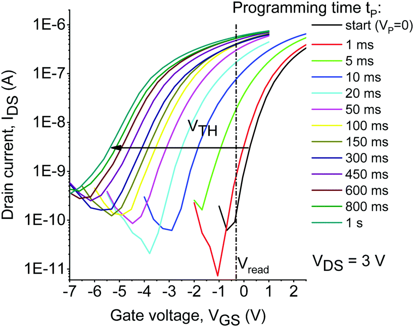 | ||
| Fig. 2 Evolution of the transfer characteristics of the devices comprising TO-2 under a negative applied voltage (VP = −5 V) and violet light (λ = 405 nm) as a function of the programming time. | ||
The switching characteristics of the devices assembled with different photochromic materials are compared in Fig. 3. The devices comprising TO-2 demonstrated the widest memory window (largest variation of VTH) and the highest switching rates under both positive and negative programming bias potentials. On the contrary, devices incorporating TO-0 with an unsubstituted cyclopentene bridge demonstrate the narrowest operation window and programming with negative bias (VP = −5 V) results in a very slow evolution of the OFET characteristics towards lower VTH voltages. Devices with the photochromic compound TO-1 enabled reasonably fast forward switching at negative VP, while the backward transition under the positive VP was extremely slow (tp > 2 s). Applying positive voltage and violet light allowed restoration of the electrical characteristics of the OFETs with TO-0 and with TO-2 to the initial state, which means complete erasing of the programmed states as required for proper functioning flash memory elements.
 | ||
| Fig. 3 Evolution of the drain currents at Vread (a) and the device threshold voltages (b) under the negative (programming, closed symbols) and positive (erasing, hollow symbols) bias potentials applied simultaneously with violet light (λ = 405 nm) as a function of the programming time. The arrows indicate the characteristic times required to achieve threshold voltage shifts of 1.5 V. | ||
On the contrary, we were not able to switch the devices with TO-1 back to the initial state with the erase voltage of +5 V. Therefore, under the specified conditions the devices based on TO-1 operate as read-only memories (ROM).
The obtained results clearly show that the chemical structure of the photochromic material has a strong impact on the device performance and, most probably, the incorporation of the carbonyl groups enhances the responsivity of the OFET towards optoelectrical programming, while the position of the carbonyl function affects reversibility of the switching.
We also explored the hysteresis effects occurring under stepwise programming with either positive or negative bias combined with the light. While performing this experiment, the programming voltage VP was swept in the range from −7 V to +9 V while fixing the light exposure time at tp = 100 ms. Fig. 4 shows the dependence of the device threshold voltages on the applied programming potentials. The series of transfer characteristics obtained in the experiment are shown in Fig. S8–S10 (ESI†).
 | ||
| Fig. 4 Evolution of the OFET threshold voltages as a function of the programming voltage for the systems comprising TO-0 (green), TO-1 (blue) and TO-2 (red) photochromic molecules. The arrows along lines show a direction of programming voltage changes during an experiment from start to end. | ||
The devices assembled with the photochromic materials TO-1 and TO-2 with carbonyl functional groups operated mostly within the negative threshold voltage domain thus suggesting the accumulation of negative charge carriers in the channel of the transistors. The charge accumulation (or trapping) is also evident from a noticeable hysteresis in the VTHvs. VP dependences. Interestingly, the devices based on the carbonyl-free TO-0 compound did not show any VTH shifts at the relatively short programming time of 100 ms. As a clear conclusion, electron accumulation in the OFET channel can be associated with the presence of carbonyl groups in the photochromic molecule (see discussion of the mechanism below).
At the final stage, we explored write–read–erase cycling performance and retention characteristics of the memory devices. By optimizing the programming conditions (bias voltage and exposure time), we were able to achieve a fully reversible switching of OFETs between two distinct electrical states for all three photochromic materials (Fig. 5).
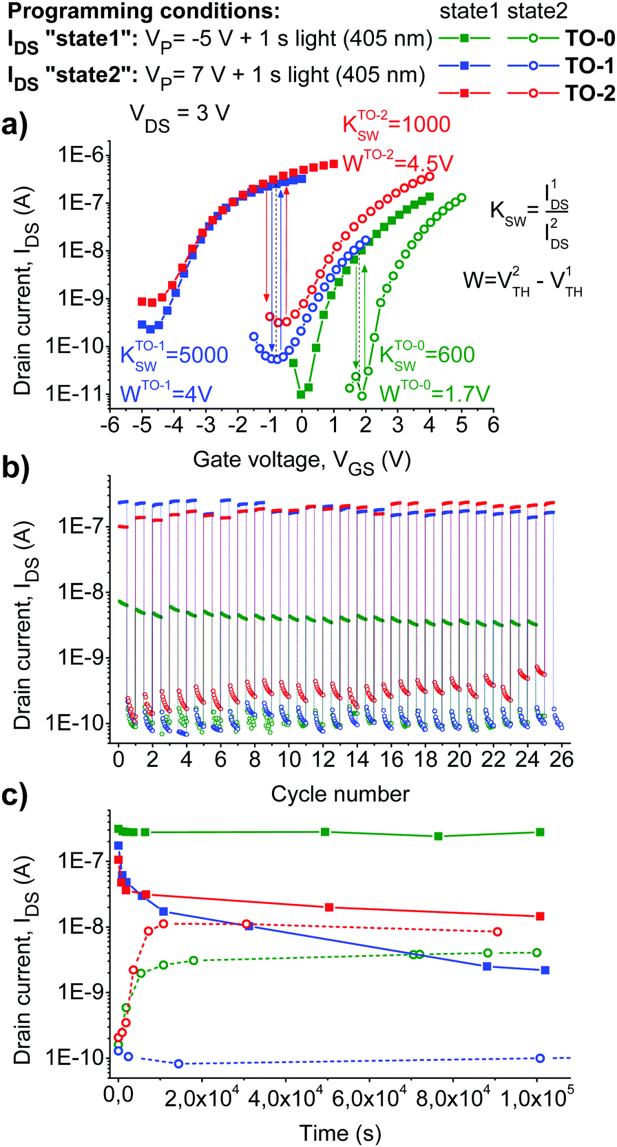 | ||
| Fig. 5 Switching OFETs with different photochromic materials between two distinct electrical states (a). Write–read–erase cycling behavior of the devices (b) and their retention characteristics (c). | ||
Both TO-1 and TO-2 compounds enabled device operation within negative VTH domain (electrons accumulated in the channel), while using TO-0 lead to positive VTH values suggesting the accumulation of positive charge carriers in the transistor channel. It is seen from Fig. 5 that devices based on the photochromic materials TO-1 and TO-2 have wide memory windows (W ≈ 4 V) and switching coefficients (KSW = IDS(state 1)/IDS(state 2) ≈ 1000–5000). The switching coefficients for the devices comprising TO-0 were one order of magnitude lower, while still sufficient for memory cell applications.
To apply photoswitchable OFETs as memory devices, they should have sufficient retention characteristics, i.e. the induced electrical states should be stable in time. In order to check the device stability, the evolution of the transfer characteristics of OFETs in time for >106 s was investigated (Fig. 5c). The highest stability of the electrical states was revealed for the devices incorporating photochromic compound TO-0. On the contrary, the OFETs loaded with the compound TO-1 showed very poor retention characteristics. Severe fading effects were also revealed for OFETs comprising TO-2. Thus, the obtained results suggest that probably only the devices incorporating TO-0 are suitable for memory technology applications.
To understand the different behavior of the explored photochromic materials in photo-switchable OFETs, we investigated interactions of diarylethenes TO-0, TO-1, and TO-2 with the semiconductor material represented by the [60]fullerene. We showed previously that there is a possibility for photoinduced charge separation in the C60-dihetarylethene system and the formed radical-ion species might be revealed by light-enhanced electron spin resonance (LESR) spectroscopy.37 Probably, similar processes occur also in the devices comprising photochromic compounds explored in this work.
Indeed, C60 film has a relatively low absorbance (ranging from 0.15 to 0.49, Fig. S11, ESI†) at 405 nm, which means that it is semitransparent and the programming laser beam can approach the fullerene/dihetarylethene interface and induce photoinduced charge separation.
To probe the system with LESR, we prepared a film of the model TO-1 + C60 + [60]PCBM (1:1:1 w/w/w) composite, where fullerene derivative [60]PCBM was added to improve the miscibility of the fullerene and dihetarylethene components. The presence of [60]PCBM should not confuse the measurement results, since this derivative has lower electron affinity as compared to the parent fullerene C60.
Fig. 6 shows the ESR spectra of the TO-1 + C60 + [60]PCBM blend recorded in the dark and under illumination. No signals were observed in the dark even at a low temperature of 123 K. However, a clear signal with g = 2.0001 and ΔH = 0.28 mT characteristic for the C60˙− radical anion appeared in the ESR spectra under violet light illumination (405 nm). Such a change in the spectra indicates the photoinduced charge separation leading to the formation of ionic pairs [TO-1˙+⋯C60˙−]. This signal completely disappears after keeping the samples at room temperature for 10–20 min, which points to the reversibility of the charge separation. It should be emphasized that the single-component films of individual C60 or TO-1 do not show any light-induced ESR signals (Fig. S12, ESI†). Thus, the obtained results confirm that the photoinduced charge separation between the photochromic material (electron donor) and fullerene semiconductor (acceptor) might represent the first stage of the device switching mechanism.
 | ||
| Fig. 6 ESR spectra of the TO-1 + C60 + [60]PCBM composite films recorded at 123 K in the dark (1), under illumination with violet light (2) and after annealing the sample at room temperature (3). | ||
To address further the mechanistic aspects of the OFET light-induced switching reported in this work, we should consider separately the systems comprising TO-1 and TO-2vs. the system incorporating TO-0 since they operate in different regimes as clearly seen from Fig. 5a. Indeed, the devices with TO-1 and TO-2 work at negative VTH voltages thus implying the accumulation of the negative charge carriers in the OFET channel at the programming step.
Since programming is achieved by simultaneous application of light (charge separation) and negative gate bias, we can assume that positive charge carriers formed in the photochromic layer after charge separation move deeper towards the gate electrode and get trapped in the dielectric (e.g. at the photochromic compound/Al2O3 interface or even penetrate into oxide layer). The negative charge carriers remain stabilized at the semiconductor/dielectric interface and this stabilization is obviously related to the presence of carbonyl CO groups in TO-1 and TO-2 since TO-0 failed to provide any similar effect. It is very probable that the fullerene radical anion can undergo reversible nucleophilic addition to the carbonyl group of the photochromic compound thus forming an O-centered anion, which is much more stable than the fullerene carbanion (Fig. 7a). The formation of such anions in the channel of the transistor keeps it open even at zero VGS voltage, which manifests the programming effect. At the erasing step, we apply positive VP bias to the gate electrode in combination with light, which leads to detrapping of positive charges from the dielectric, their diffusion toward the semiconductor in the electric field and recombination with the negative charge carriers accumulated in the channel of the device. Thus, we erase the programming effect by returning the transistor to its initial state. This mechanism fully explains the switching behaviour of the devices with TO-1 and TO-2 as illustrated in Fig. 7b.
 | ||
| Fig. 7 Proposed mechanisms for the stabilization of the negative charge involving addition of a fullerene anion radical to the CO group of TO-2 and the stabilization of the positive charge via oxidative cyclization of TO-0 (a). Schematic switching mechanism for OFETs comprising TO-1 or TO-2 (b). | ||
In the case of TO-0, obviously, another mechanism is realized. Since the OFETs comprising TO-0 operate at positive VTH voltages, the programming event is accompanied by the accumulation of holes in the channel of the device. This means that programming with light (generation of charge separated states) while applying a positive VP bias to the gate electrode leads to migration and trapping of negative charge carriers in the dielectric. Meanwhile, the positive charge carriers become stabilized on the photochromic molecules presumably due to the oxidation-induced cyclization reaction reported previously for other dihetarylethenes38–40 (Fig. 7a). The erasing process under negative VP bias results in detrapping of electrons, their moving to the dielectric/semiconductor interface and quenching of the holes accumulated in the channel of the OFET. This mechanism shown in Fig. S13 (ESI†) is fully consistent with all experimental data obtained for devices incorporating TO-0 as a light-sensitive material.
To summarize, the operation mechanism of the photoswitchable OFETs with photochromic materials is not based just on simple cyclization–cycloreversion reaction. As shown here, it involves a combination of photoinduced charge separation, tunneling and trapping effects.
Conclusions
We have shown that a relatively minor modification of the photochromic dihetarylethenes by introducing a carbonyl group to the bridge part of the molecule alters completely the operation mode of the photo-switchable OFETs. Moreover, simply changing the position of the carbonyl group in the dihetarylethene core has a significant effect on the reversibility of the switching, operation speed and retention characteristics of the memory devices. The revealed effects evidence that modification of the chemical structure of the photochromic component represents a powerful approach for tuning the characteristics of light-switchable OFETs to deliver advanced organic memory devices with excellent electrical characteristics, long-term retention and good write–read–erase cycling stability.Conflicts of interest
There are no conflicts to declare.Acknowledgements
This work was supported by the Russian Foundation for Basic Research (grant no. 18-33-00904) and Russian Ministry for Science and Education (project No. 0089-2019-0010). Synthesis of photochromic diarylethenes was supported by Russian Science Foundation (grant no. 18-73-00290).Notes and references
- Y. van de Burgt, A. Melianas, S. T. Keene, G. Malliaras and A. Salleo, Nat. Electron., 2018, 1, 386–397 CrossRef.
- C. Wang, C. Wang, Z. Huang and S. Xu, Adv. Mater., 2018, 30, 1801368 CrossRef.
- D. Luo, Q. Chen, B. Liu and Y. Qiu, Polymers, 2019, 11, 384 CrossRef.
- R. Xue, J. Zhang, Y. Li and Y. Li, Small, 2018, 14, 1801793 CrossRef PubMed.
- S. Ishihara, J. Labuta, W. Van Rossom, D. Ishikawa, K. Minami, J. P. Hill and K. Ariga, Phys. Chem. Chem. Phys., 2014, 16, 9713 RSC.
- P. C. Y. Chow, N. Matsuhisa, P. Zalar, M. Koizumi, T. Yokota and T. Someya, Nat. Commun., 2018, 9, 4546 CrossRef PubMed.
- J. Meena, S. Sze, U. Chand and T.-Y. Tseng, Nanoscale Res. Lett., 2014, 9, 526 CrossRef PubMed.
- M. Ghoneim and M. Hussain, Electronics, 2015, 4, 424–479 CrossRef CAS.
- K. Qian, V. C. Nguyen, T. Chen and P. S. Lee, J. Mater. Chem. C, 2016, 4, 9637–9645 RSC.
- L. Zhou, J. Mao, Y. Ren, S.-T. Han, V. A. L. Roy and Y. Zhou, Small, 2018, 14, 1703126 CrossRef.
- Y.-H. Chou, H.-C. Chang, C.-L. Liu and W.-C. Chen, Polym. Chem., 2015, 6, 341–352 RSC.
- L. Xiang, W. Wang and W. Xie, Sci. Rep., 2016, 6, 36291 CrossRef CAS PubMed.
- C. Wang, P. Gu, B. Hu and Q. Zhang, J. Mater. Chem. C, 2015, 3, 10055 RSC.
- S.-P. Cho, S. Jang, H.-N. Jo, S.-A. Lee, S. Bae, S. H. Lee, J. Hwang, H.-I. Joh, G. Wang and T.-W. Kim, J. Mater. Chem. C, 2016, 4, 1511 RSC.
- G. Wang, X. Liu and W. Wang, IEEE Electron Device Lett., 2018, 39, 111 CAS.
- E. Orgiu and P. Samorì, Adv. Mater., 2014, 26, 1827–1845 CrossRef CAS PubMed.
- Y. Wakayama, R. Hayakawa and H.-S. Seo, Sci. Technol. Adv. Mater., 2014, 15, 024202 CrossRef PubMed.
- X. Zhang, L. Hou and P. Samorì, Nat. Commun., 2016, 7, 11118 CrossRef CAS PubMed.
- J. Zhang and H. Tian, Adv. Opt. Mater., 2018, 6, 1701278 CrossRef.
- H. Cheng, J. Yoon and H. Tian, Coord. Chem. Rev., 2018, 372, 66–84 CrossRef CAS.
- L. Sun, S. Wang and H. Tian, Chem. Lett., 2007, 36, 250–251 CrossRef CAS.
- Y. Wu, Y. Xie, Q. Zhang, H. Tian, W. Zhu and A. D. Q. Li, Angew. Chem., Int. Ed., 2014, 53, 2090–2094 CrossRef CAS.
- T. Biellmann, A. Galanti, J. Boixel, J. A. Wytko, V. Guerchais, P. Samorì and J. Weiss, Chem. – Eur. J., 2018, 24, 1631–1639 CrossRef CAS PubMed.
- M. Döbbelin, A. Ciesielski, S. Haar, S. Osella, M. Bruna, A. Minoia, L. Grisanti, T. Mosciatti, F. Richard, E. A. Prasetyanto, L. De Cola, V. Palermo, R. Mazzaro, V. Morandi, R. Lazzaroni, A. C. Ferrari, D. Beljonne and P. Samorì, Nat. Commun., 2016, 7, 11090 CrossRef PubMed.
- K. Boerjesson, M. Herder, L. Grubert, D. T. Duong, A. Salleo, S. Hecht, E. Orgiu and P. Samori, J. Mater. Chem. C, 2015, 3, 4156–4161 RSC.
- T. Mosciatti, M. G. del Rosso, M. Herder, J. Frisch, N. Koch, S. Hecht, E. Orgiu and P. Samorì, Adv. Mater., 2016, 28, 6606–6611 CrossRef CAS PubMed.
- T. Leydecker, M. Herder, E. Pavlica, G. Bratina, S. Hecht, E. Orgiu and P. Samorì, Nat. Nanotechnol., 2016, 11, 769 CrossRef CAS PubMed.
- M. E. Gemayel, K. Börjesson, M. Herder, D. T. Duong, J. A. Hutchison, C. Ruzié, G. Schweicher, A. Salleo, Y. Geerts, S. Hecht, E. Orgiu and P. Samorì, Nat. Commun., 2015, 6, 6330 CrossRef PubMed.
- R. Hayakawa, M. Petit, K. Higashiguchi, K. Matsuda, T. Chikyow and Y. Wakayama, Org. Electron., 2015, 21, 149–154 CrossRef CAS.
- T. Tsuruoka, R. Hayakawa, K. Kobashi, K. Higashiguchi, K. Matsuda and Y. Wakayama, Nano Lett., 2016, 16, 7474–7480 CrossRef CAS PubMed.
- Y. Kurokawa, R. Hayakawa, S. Shimada, K. Higashiguchi, Y. Noguchi, K. Matsuda and Y. Wakayama, Org. Electron., 2019, 64, 205–208 CrossRef CAS.
- A. G. Lvov, M. M. Khusniyarov and V. Z. Shirinian, J. Photochem. Photobiol., C, 2018, 36, 1–23 CrossRef CAS.
- L. A. Frolova, P. A. Troshin, D. K. Susarova, A. V. Kulikov, N. A. Sanina and S. M. Aldoshin, Chem. Commun., 2015, 51, 6130 RSC.
- L. A. Frolova, A. A. Rezvanova, B. S. Lukyanov, N. A. Sanina, P. A. Troshin and S. M. Aldoshin, J. Mater. Chem. C, 2015, 3, 11675 RSC.
- A. G. Lvov, E. Yu. Bulich, A. V. Metelitsa and V. Z. Shirinian, RSC Adv., 2016, 6, 59016–59020 RSC.
- V. Z. Shirinian, A. G. Lvov, M. M. Krayushkin, E. D. Lubuzh and B. V. Nabatov, J. Org. Chem., 2014, 79, 3440–3451 CrossRef CAS.
- L. A. Frolova, A. A. Rezvanova, V. Z. Shirinian, A. G. Lvov, A. V. Kulikov, M. M. Krayushkin and P. A. Troshin, Adv. Electron. Mater., 2016, 2, 1500219 CrossRef.
- T. Nakashima, Y. Kajiki, S. Fukumoto, M. Taguchi, S. Nagao, S. Hirota and T. Kawai, J. Am. Chem. Soc., 2012, 134, 19877–19883 CrossRef CAS.
- J. Massaad, J.-C. Micheau, C. Coudret, C. L. Serpentini and G. Guirado, Chem. – Eur. J., 2013, 19, 12435–12445 CrossRef CAS PubMed.
- M. Herder, M. Utecht, N. Manicke, L. Grubert, M. Patzel, P. Saalfrank and S. Hecht, Chem. Sci., 2013, 4, 1028–1040 RSC and references therein.
Footnote |
| † Electronic supplementary information (ESI) available: Experimental procedures, and transfer characteristics of OFETs under various conditions. See DOI: 10.1039/c9tc01273g |
| This journal is © The Royal Society of Chemistry 2019 |