
Radiation damage effects in Ga2O3 materials and devices
Jihyun
Kim
 *a,
Stephen J.
Pearton
b,
Chaker
Fares
c,
Jiancheng
Yang
c,
Fan
Ren
c,
Suhyun
Kim
a and
Alexander Y.
Polyakov
d
*a,
Stephen J.
Pearton
b,
Chaker
Fares
c,
Jiancheng
Yang
c,
Fan
Ren
c,
Suhyun
Kim
a and
Alexander Y.
Polyakov
d
aDepartment of Chemical & Biological Engineering, Korea University, Anam-dong, Sungbuk-gu, Seoul, Korea. E-mail: hyunhyun7@korea.ac.kr
bDepartment of Materials Science and Engineering, University of Florida, Gainesville, FL 32606, USA
cDepartment of Chemical Engineering, University of Florida, Gainesville, FL 32606, USA
dNational University of Science and Technology MISiS, Leninsky Ave. 4, Moscow, 119049, Russia
First published on 19th October 2018
Abstract
The strong bonding in wide bandgap semiconductors gives them an intrinsic radiation hardness. Their suitability for space missions or military applications, where issues of radiation tolerance are critical, is widely known. Especially β-Ga2O3, an ultra-wide bandgap material, is attracting interest for power electronics and solar-blind ultraviolet detection. Beside its superior thermal and chemical stabilities, the effects of radiation damage on Ga2O3 are of fundamental interest in space-based and some terrestrial applications. We review the effect on the material properties and device characteristics of proton, electron, X-ray, gamma ray and neutron irradiation of β-Ga2O3 electronic and optoelectronic devices under conditions relevant to low earth orbit of satellites containing these types of devices.
 Jihyun Kim | Jihyun Kim is a Professor of the Department of Chemical and Biological Engineering at Korea University. He received his BS from Department of Chemical Engineering, Seoul National University, Korea, and PhD from Department of Chemical Engineering, University of Florida, USA in 2004. He did his internship at Bell Laboratories in Murray Hill. Then, he joined US Naval Research Laboratory in Washington, DC to work on the optical characterizations of wide-bandgap semiconductors. His interests are in the electronic/optical properties and device fabrications of wide-bandgap semiconductors and two-dimensional materials. |
 Stephen J. Pearton | Stephen J. Pearton is Distinguished Professor and Alumni Chair of Materials Science and Engineering at the University of Florida, Gainesville, FL, USA. He has a PhD in Physics from the University of Tasmania and was a postdoc at UC Berkeley prior to working at AT&T Bell Laboratories in 1994–2004. His interests are in the electronic and optical properties of semiconductors. He is a Fellow of the IEEE, AVS, ECS, TMS, MRS, SPIE and APS. He was the recipient of the 2007 J. J. Ebers Award from IEEE. |
 Chaker Fares | Chaker Fares is a PhD student fellow in the Department of Chemical Engineering at the University of Florida. He has a bachelor's degree from the Georgia Institute of Technology. His research interests include compound semiconductor fabrication/characterization and renewable energy technologies. |
 Jiancheng Yang | Jiancheng Yang is a graduate student fellow in the Department of Chemical Engineering, University of Florida, Gainesville. His research interests include the fabrication and characterization of compound semiconductor devices and bio-sensors. |
 Fan Ren | Fan Ren is Distinguished Professor and Fred and Bonnie Edie Professor of Chemical Engineering at the University of Florida, Gainesville, FL, USA. He joined UF in 1997 after 12 years as a Member of Technical Staff at AT&T Bell Laboratories, where he was responsible for high speed compound semiconductor device development. He is a Fellow of ECS, MRS, IEEE, SPIE, APS and AVS. |
 Alexander Y. Polyakov | Alexander Y. Polyakov is a Professor at the Department of Semiconductor Electronics and Physics of Semiconductors of the National University of Science and Technology (MISiS) in Moscow and head of the laboratory “Wide-Bandgap Semiconductors and Devices”. He graduated from MISiS in 1973, worked at the Institute of Rare Metals in Moscow, at Carnegie Mellon University in the USA and Chonbuk National University at South Korea on materials science of III–V and II–VI semiconductors. He is an author or co-author of more than 300 papers, 2 monographs, multiple invited chapters in books on III–V semiconductors, and multiple review articles. |
Introduction
β-Ga2O3 is gaining attention because of its large bandgap of 4.8–4.9 eV and high estimated critical electric field (Ec) strength of ∼8 MV cm−1.1–21 The large bandgap allows extending device operation to high temperatures, while the large critical field allows high voltage operation.1,2,4,6Fig. 1 (top) shows how this translates to potentially higher switching performance than other wide bandgap materials including GaN or SiC. Only diamond and AlN have higher figures-of-merit, but issues with cost and conductivity, respectively, limit their applicability.1,10 The main electronics applications for β-Ga2O3 rectifiers and metal-oxide–semiconductor field effect transistors (MOSFETs) involve power conditioning and switching systems with low power loss during high frequency switching up to the GHz regime.6,9,10 On the detector side, Ga2O3-based photodetectors are attracting interest as truly solar-blind deep ultraviolet (UV) photodetectors, since they exhibit cut-off wavelengths below 280 nm and have applications in military systems, air purification, space communication, ozone-layer monitoring and flame sensing.11,12Fig. 1 (bottom) shows the wavelength range covered by Ga2O3 and the related ternary alloys involving In or Al. The true solar-blindness of photodetectors based on β-Ga2O3 means they do not require any supplementary filter, in contrast to the case of GaAs or Si detectors.11,12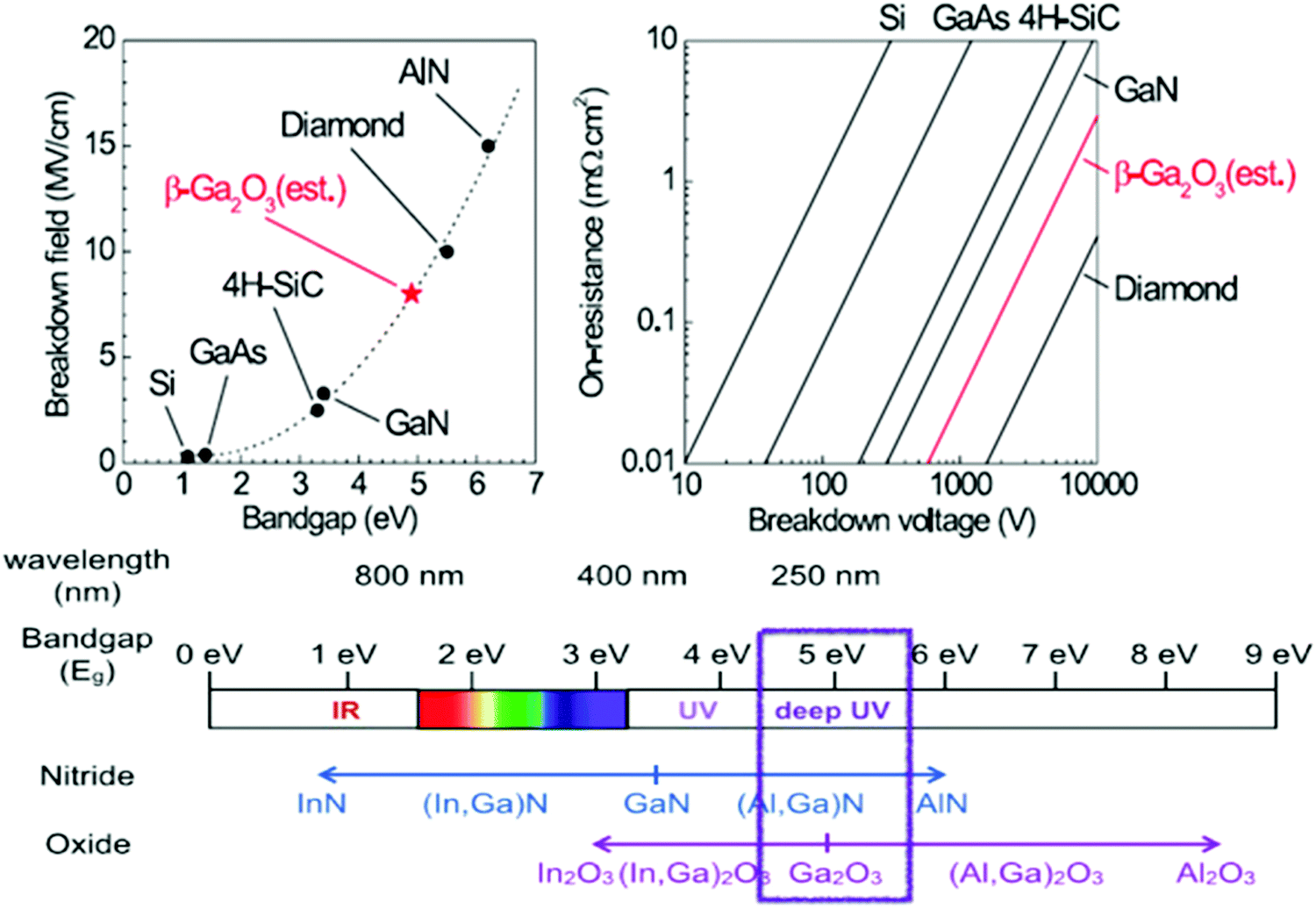 | ||
| Fig. 1 Breakdown voltages and on-state resistances for power electronic devices fabricated on different semiconductors (top) and schematic of bandgaps and equivalent wavelengths spanned by the range of compositions of both the GaN and the Ga2O3-based family of materials with their associated Al and In-containing ternary alloys (bottom). | ||
A huge advantage for β-Ga2O3 in these applications is the availability of large diameter wafers. Bulk crystals have been grown by all the common techniques, including the Czochralski (CZ), float-zone (FZ), edge-defined film fed (EFG) or Bridgman (horizontal or vertical, HB and VB) growth methods.2,7,19,20 Wafers from these bulk crystals can obviously be used for devices like rectifiers, but also provide a template for growth of epitaxial films of controlled thickness and doping for active channel and contact layers5,8,14,15,21 to allow achievement of targeted device parameters such as breakdown voltage, on-state resistance and reverse recovery time.
The robustness of wide bandgap materials is especially advantageous in harsh environments caused by high temperature, pressure or radiation. Given the potential applications for Ga2O3 photoconductors and electronics, they could be subject to fluxes of high energy protons, alpha particles and electrons if used in low earth orbit satellites, as well as neutrons or gamma rays if used in radiation-hard nuclear or military systems.22–28 Each of these forms of radiation produces different types of crystal lattice damage on the crystalline materials. In addition, primary defects may recombine, and form complexes with each other, with dopants and with extended defects.29–33 This may be more complicated in β-Ga2O3, which has two crystallographically inequivalent Ga positions, one with tetrahedral geometry, known as Ga(I), and one with octahedral geometry, known as Ga(II).3,7,9,34 Similarly, the oxygen atoms have three crystallographically different positions denoted as O(I), O(II) and O(III), respectively. Two oxygen atoms are coordinated trigonally and one is coordinated tetrahedrally. The lattice structure is shown schematically in Fig. 2(a), while the two major crystal planes used for devices are shown in Fig. 2(b). This complexity means there are a larger number of possible defect complexes that could form upon irradiation.
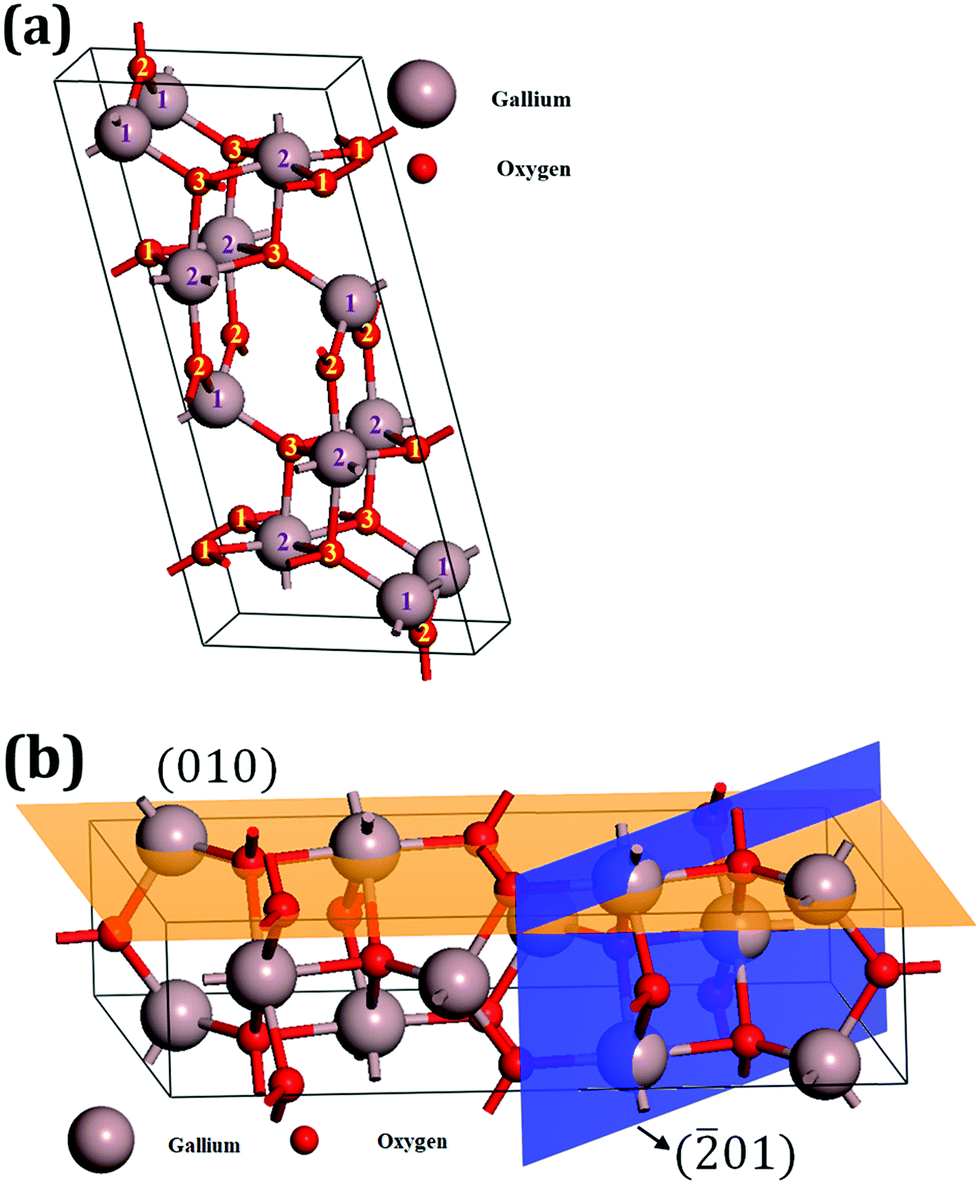 | ||
Fig. 2 (a) β-Ga2O3 crystal structure and (b) (010) and (![[2 with combining macron]](https://www.rsc.org/images/entities/char_0032_0304.gif) 01) surfaces. Reprinted with permission from Pearton et al.,9 copyright 2018, American Institute of Physics. 01) surfaces. Reprinted with permission from Pearton et al.,9 copyright 2018, American Institute of Physics. | ||
At high incident energies, the energy of the primary recoils formed by collisions with lattice atoms becomes so high that they produce collision cascades and form heavily disordered regions (domains) with a very high defect density in the core.29–31,35,36 The collision between an incoming ion and a lattice atom displaces the atom from its original lattice position, leading to vacancies, interstitials and complexes of both, and potentially with impurities in the Ga2O3.37,38 If an incident energetic particle such as a neutron or proton collides with the nucleus of a lattice atom, the primary knock-on atom may be displaced from the lattice if the incident particle has sufficient energy (E > Ed), where Ed is the lattice displacement energy.28–30
Importance of radiation damage in electronics
There are a number of fundamental material parameters important in radiation damage studies, including the ionization energy and capture cross section of the hole or electron traps created and the carrier removal rate for each type of incident radiation, which will determine the lifetime of electronics in radiation environments. These are of interest because of the space radiation encountered by satellites,39 potential high altitude nuclear explosions and robotic inspection systems used near reactor cores or in accident response. The main concerns are the response of electronics to total ionizing dose displacement damage (crystal and interface damage) and single event effects (transients and bit flips due to single energetic particles).22–29For space-based applications, it is of note that the Earth is surrounded by two regions (the Van Allen radiation belts) containing charged particles trapped in the Earth's magnetic field.39 The inner belt, extending from 1200–6500 km (2.5 Earth radii) above the Earth's surface, is relatively stable whereas the outer belt, which extends from 13![[thin space (1/6-em)]](https://www.rsc.org/images/entities/char_2009.gif) 000–40000 km (10 Earth radii), is highly variable. The belts are separated by a gap, known as the slot region, containing few energetic electrons (Fig. 3). The high-energy ionizing particles in this space environment are responsible for the anomalies observed in electronics and fall into three categories:22–27
000–40000 km (10 Earth radii), is highly variable. The belts are separated by a gap, known as the slot region, containing few energetic electrons (Fig. 3). The high-energy ionizing particles in this space environment are responsible for the anomalies observed in electronics and fall into three categories:22–27
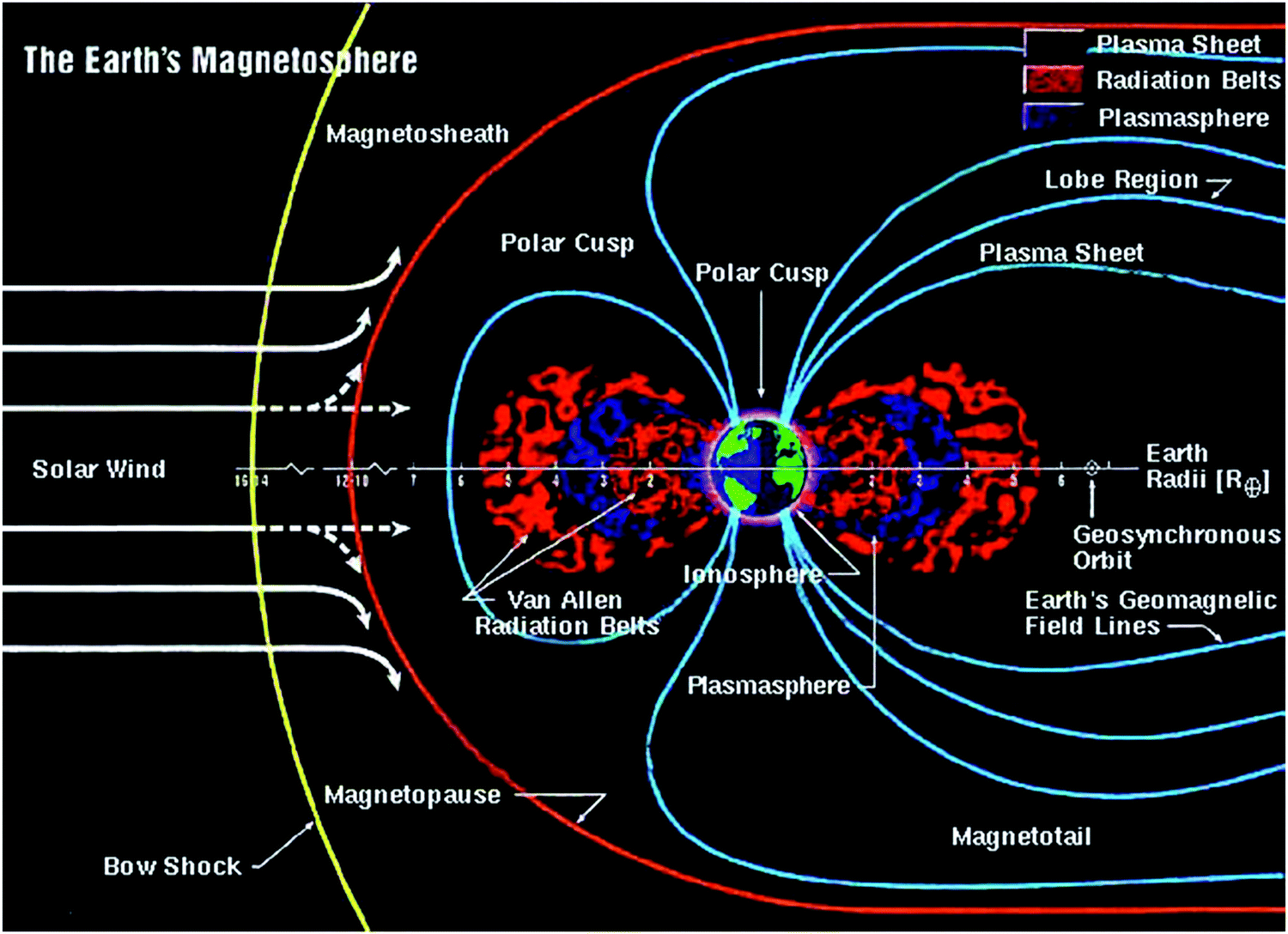 | ||
| Fig. 3 Schematic of space radiation effects in the magnetosphere, Space Environments & Effects Program, NASA Marshall Space Flight Center http://holbert.faculty.asu.edu/eee560/spacerad.html. | ||
(i) The Van Allen belts containing charged particles like electrons and protons. The inner belt comprises protons up to 600 MeV and electrons up to several MeV, while the outer belt has electrons and protons (0.1 to 5 MeV). The slot region between the belts may be enhanced for a year following solar events. These events last several days and comprise both protons and heavier ions. Energies range up to several hundred MeV.39
(ii) Solar flares producing protons (up to 500 MeV) and a smaller component of heavy ions (up to 10 MeV per nucleon). The flare occurrence is influenced by the solar cycle.40
(iii) Cosmic rays, originating outside the solar system, leading to a continuous background of ions whose energies can be very high. The Earth's magnetosphere is bombarded by this nearly isotropic flux of energetic charged particles – 85% protons, 14% α-particles, and 1% heavier ions covering the full range of elements. These are partly kept out by the Earth's magnetic field. Primary cosmic rays interact with air nuclei to generate a cascade of secondary particles comprising protons, neutrons, mesons and nuclear fragments. The intensity of radiation is a maximum at 18 km and drops off to sea level. At normal aircraft cruising altitudes the radiation is several hundred times the ground level intensity and at 18 km a factor of three higher.41–44
Neutron irradiation tends to create disordered regions in semiconductors, while the damage from the other forms of radiation is more typically point defects. In all cases, the damaged region contains carrier traps that reduce the conductivity of the semiconductor and at high enough doses, cause severe degradation of device performance.30–33,45,46 The behavior of neutral radiation like gamma rays passing through semiconductors is fundamentally different than the interaction with charged particles such as protons, electrons or alpha particles and the energy loss mechanisms are the photoelectric effect, Compton scattering and pair production for γ- and X-rays while nuclear (“billiard-ball collisions”) and electronic loss (ionization, heat) are the dominant mechanisms for ionizing radiation.29–36
These particles produce various effects on semiconductor devices, including the accumulation of ionizing dose deposition over a long period, known as the total ionizing dose (TID) effect.40–44 This mainly results from the most prevalent particles (electrons and protons) and leads to degradation of the electrical performance of devices. The accumulation of non-ionizing dose deposition due to protons or high energy electrons generates lattice defects leading to displacement damage effects (DD). These are critical in some classes of devices (sensors, charge-coupled devices, amplifiers) and induce degradation of electrical parameters or increased background noise. Finally, there are the transient effects from a single particle in sensitive regions of devices, called Single Event Upsets or Effects (SEU or SEE).29,39–45 This instantaneous perturbation is due to protons and heavy ions and leads to functional anomalies in most kinds of devices.41–44
For all of the ionizing particles within the atmosphere, the particle energy and flux vary with altitude and latitude.39 The rate of SEUs observed in avionics correlates with the atmospheric neutron flux created by the interaction of cosmic rays with the oxygen and nitrogen atoms in the air at elevated altitudes.40,41 The major concern in this case is random access memories (RAMs), both static and dynamic RAMs, because these contain the largest number of bits susceptible to upset.23–27 The common method for dealing with SEU in RAMs is by error detection and correction (EDAC).27 Commercially available computer systems for aircraft incorporate EDAC in their designs. In addition to upset, other SEEs, such as latch-up and burnout, although less probable, also cause concern.23–26 Charged particles in the atmosphere are also reaction products from the interaction of the primary cosmic rays with the O and N nuclei in the air. These include protons, pions, kaons, and electrons, with the pions and kaons decaying to muons. Most focus is on protons since they also cause SEEs.39,41,42 The distribution of protons is similar to that of neutrons, with respect to energy and altitude.39 The flux of the heavy ions within the primary cosmic rays is rapidly attenuated with increasing atmospheric depth due to interactions with the atmosphere that fragment and thereby remove these heavy ions.39
Most telecommunications satellites are located in geosynchronous orbit (Geo), located at the outer edge of the outer radiation belt.39 Most navigation satellites, such as GPS and Galileo, operate in medium Earth orbit and pass through the heart of the outer radiation belt where they may subsequently experience much higher levels of radiation. Most Earth-observation satellites operate in low Earth orbit and may experience higher radiation levels if their orbits traverse the South Atlantic Anomaly or the auroral zones. The variability in flux of relativistic electrons (E > 1 MeV) in the radiation belts is caused by changes in the solar wind by activity on the Sun.
The types of radiation damage suffered by microelectronics are:22–29
(i) Total dose effects – usually the factor that limits the operational lifetime of spacecraft electronics. As the dose accumulates, the changes in electrical properties of the semiconductor drive the component parameters outside of the design range for the circuits in which they are used and cause the circuit to cease proper functioning.
(ii) Displacement damage, a cumulative effect resulting from prolonged exposure to the radiation environment. Displacement damage is caused by relatively low-energy atomic particles, as they transfer energy to the semiconductor lattice. These low-energy particles may be either directly present in the environment or produced indirectly by nuclear interactions in the device material or shielding. These particles displace atoms from their crystal lattice locations, creating defects in the crystal structure. These trap conduction electrons, increasing the resistance of the device.
(iii) Single event effects are changes in a microelectronic device caused by being hit by a single energetic particle.25,26 SEE are electrical noise induced by the space environment and result in data corruption, transient disturbance, and high current conditions which result in non-destructive and destructive effects. Single event upsets cause a change of state in storage elements, while Single Event Functional Interrupts (SEFI) are events leading to temporal loss of device functionality and can be recovered by reset. Single Event Transients (SET) are transients on external signals leading to erroneous data. SEFI are caused by a single ion strike, similar to the usual single event upsets in memory devices. However, SEFI are manifested in a somewhat different manner. SEFI lead to temporary non-functionality (interruption of normal operation) of the affected device. It may last as long as the power is maintained in some cases, while in others it may last for a finite period.25,26,40–44
Table 1 shows a compilation of current and future requirements for total dose and single event upset radiation hardness of microelectronics.47
| Parameter | Ultimate goal | Current requirement |
|---|---|---|
| Total ionizing dose (krad (Si)) | 103 | 3 × 10² |
| Single event upset (SEU) (errors/bit-day) | <10−11 | <10−10 |
| Single event functional interrupt (errors/chip-day) | None | <10−5 |
| Single event latch-up | None | None |
| Dose rate upset (radSi)/s | None | >108 |
| Displacement damage (n/cm2) | 1014 | 1012 |
Radiation damage in wide bandgap semiconductors
The strong bonding in wide bandgap semiconductors gives them intrinsically high radiation resistance.1,9,18,31–36,44–46 The fluence of ionizing radiation at which materials and devices such as transistors and light-emitting diodes made from SiC, GaN and related materials start to show degradation is about two orders of magnitude higher than in their GaAs equivalents.9,31–36,44–46 This difference is at least partially attributed to the stronger bonding of these materials. A measure of this bond strength is the energy required to displace an atom from its lattice position or simply the atomic displacement energy. This parameter has been measured in several semiconductors and empirically determined to be inversely proportional to the volume of the unit cell.30–32 This also generally scales with energy bandgap, so that these wide bandgap materials have intrinsically higher radiation resistance than Si. From the known size of the Ga2O3 unit lattice,3,6,7 it should be quite radiation hard. β-Ga2O3 has lattice constants of a = 12.2 Å, b = 3.0 Å, and c = 5.8 Å. As a rough estimate of the expected bond strength we take the average lattice constant of the b and c distances, i.e. 4.4 Å; we would expect a similar radiation hardness to that of GaN.29–33The displacement energy threshold plays a crucial role in determining the induced defect concentration for incident electrons having energies <750 keV. The number of Frenkel pairs Nd created by an incident particle can be approximated by Nd = κÊ/2Ed, where κ is the displacement efficiency and Ê is the energy given up in creating atomic displacements.29–33 This is referred to as the non-ionizing energy loss or the nuclear stopping component. For higher energy or heavier particles, the approximation for Nd is less accurate. However, it has been pointed out by Weaver et al.33 that while fewer defects are created in GaN than in GaAs because of the larger values of Ed, the difference (36%) is insufficient to explain the order-of-magnitude (1000%) difference in radiation tolerance. They suggested that creation of Ga vacancies, which are triple acceptors, causes the number of acceptors to significantly increase and (Nd–Na) to decrease.33 It is not yet clear whether a similar explanation can be applied to other wide bandgap materials, or this is specific to the case of GaN. However, VGa acceptors are among the dominant defects present in Ga2O3, even in the as-grown state.48–52
How do the properties of Ga2O3 relate to radiation effects? The total ionizing doses that cause charge accumulation in field oxides in metal-oxide–semiconductor (MOS)-based devices result in the well-known shifts in threshold voltage, but if Ga2O3 transistors use Schottky metal gates, this is less of an issue.1,4 There are also the SEU effects that result from the transit of energetic ions passing through the semiconductor, creating electron–hole pairs. The device structures employed in wide bandgap semiconductors involving heterostructures tend to mitigate this effect. However, Ga2O3 rectifiers use thick active layers and will be more sensitive than a high-electron-mobility transistor (HEMT)-type device. Fig. 4 shows the projected range of protons and alpha particles in Ga2O3 as a function of energy.28 Note that the ranges extend well beyond the typical active layer thicknesses of Ga2O3 rectifiers or MOSFETs. The calculated vacancy distributions are shown in Fig. 5, with an expanded view of the near-surface region. Note that these are maximum values, since defect recombination is significant in wide band gap semiconductors during irradiation.31,36,53 The thickness issue also affects dose-rate radiation effects, which are sensitive to the total volume of a device. The last issue is lattice displacements that typically create traps and recombination sites in the device that degrade the carrier density through trapping and carrier mobility, with both of these mechanisms scaling with radiation dose. Si MOSFETs also suffer from single-event burnout when the charge from an energetic ion creates sustained conduction of the inherent parasitic bipolar transistor and single-event rupture when charge build-up near the gate causes a breakdown in the gate oxide. Ga2O3 MOSFETs are not yet at the level of sophistication where this is likely to be a controlling issue.9,10 An additional factor is that wide bandgap devices generally employ higher critical fields and smaller active volumes that reduce radiation-induced charge collection.
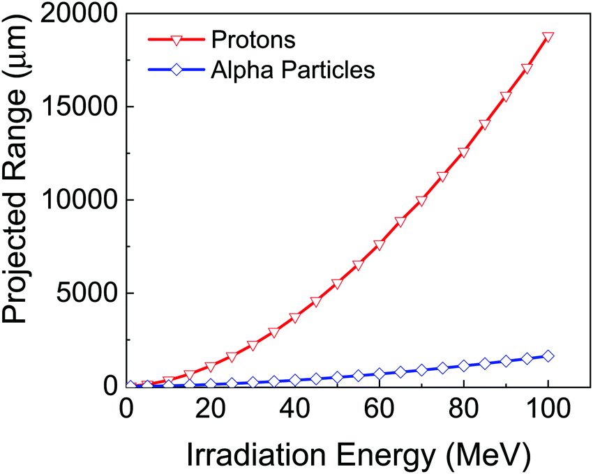 | ||
| Fig. 4 Range of protons and alpha particles in Ga2O3 as a function of energy (1–100 MeV). | ||
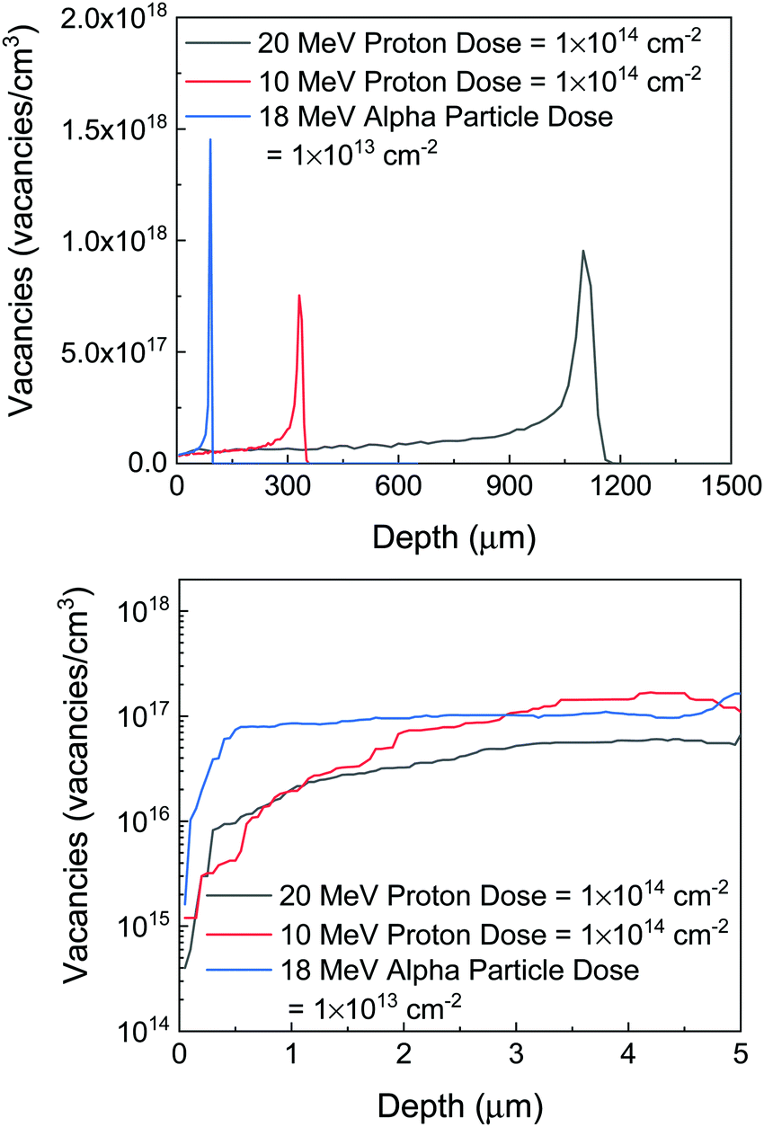 | ||
| Fig. 5 Vacancy distributions calculated by SRIM in Ga2O3 for 10 or 20 MeV protons and 18 MeV alpha particles (top) and expanded view in the region relevant for devices (bottom). | ||
Korhonen et al.48 investigated the electrical compensation in n-type Ga2O3 by Ga vacancies using positron annihilation spectroscopy. They estimated a VGa concentration of at least 5 × 1018 cm−3 in undoped and Si-doped samples. Since theoretical calculations predicts that these VGa should be in a negative charge state for n-type samples,34 they will compensate the n-type doping.48 Kananen et al.49,50 used electron paramagnetic resonance (EPR) to demonstrate the presence of both doubly ionized (V2−Ga) and singly ionized (V−Ga) acceptors at room temperature in CZ Ga2O3. They observed singly ionized gallium vacancies V−Ga in neutron irradiated β-Ga2O3. The two holes in this acceptor are trapped at individual oxygen ions located on opposite sides of the gallium vacancy. A schematic of the VGa derived from EPR is shown in Fig. 6. For the sites of interstitial Ga and O, interstitial Ga and O locate at the same site. The O vacancy, Ga vacancy, and Ga interstitial and O interstitial (NGa2O3Oi) are represented as 1, 2, and 3, respectively, in Fig. 7.54
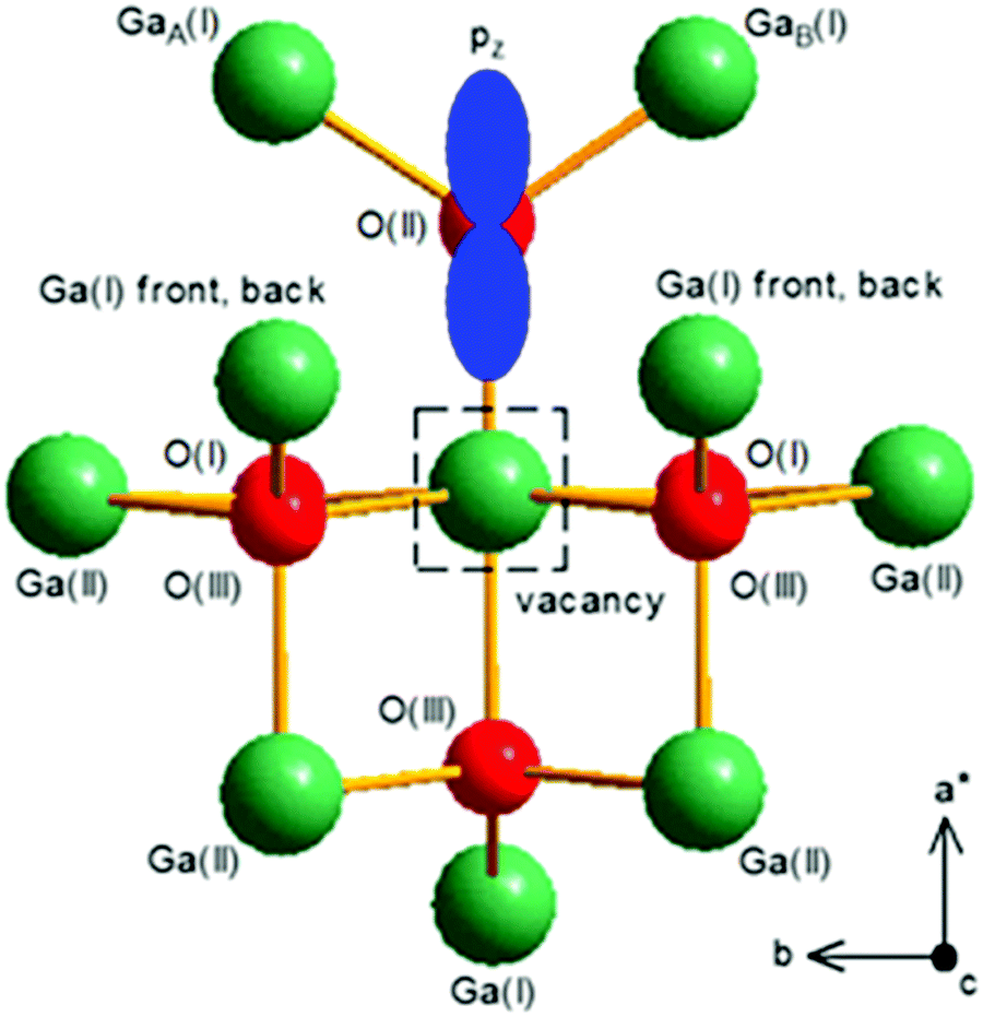 | ||
| Fig. 6 Model of the doubly ionized gallium vacancy in β-Ga2O3. An unpaired spin (the hole) is localized in a pz orbital on a threefold oxygen ion, O(II), adjacent to a gallium vacancy (dashed square) at a sixfold Ga(II) site. Reprinted with permission from Kananen et al.,49 copyright 2017 American Institute of Physics. | ||
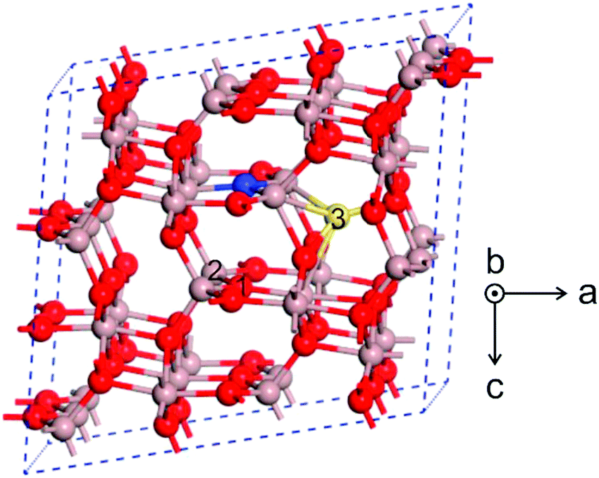 | ||
| Fig. 7 Schematic of O and Ga defects in the Ga2O3 lattice. The Ga, O and N atoms are demonstrated by brown, red and blue spheres, respectively. Numbers 1 and 2 represent the vacancy sites of O and Ga, respectively. The yellow sphere labelled with number 3 denotes the interstitial sites for both O and Ga. Reprinted with permission from Dong et al.,54 copyright 2017, Elsevier. | ||
Summary of radiation damage studies in Ga2O3
(i) Neutron damage effects
Cojocaru37 reported the effect of fast neutrons on the electrical conductivity and thermoelectric power in β-Ga2O3. The conductivity was found to decrease while the thermoelectric power increased after irradiation of 1017 cm−2. This was explained by assuming that the defects introduced acted as electron traps. The defects annealed out at 1000 K with an activation energy of 2 eV and were assumed to be most likely VGa. Arehart et al.55,56 irradiated n-Ga2O3 with 2 MeV neutrons to a fluence of 4 × 1015 cm−2. This produced a decrease in reverse current in rectifier structures, a loss of carriers at a rate of ∼20 cm−1 and the introduction of a deep trap state at Ec-1.88 eV observed in deep level transient spectroscopy (DLTS) measurements. This was tentatively ascribed to an oxygen-vacancy related state.Ga2O3 was also investigated for detection for fast (14 MeV) neutrons,57 utilizing the 16O (n,α)13C reaction. Diamond and 4H-SiC have previously been investigated as nuclear detectors under extreme conditions, involving temperatures up to 700 °C for 4H-SiC and 200 °C for diamond.57 These temperature limits are limited by contacts and packaging rather than the intrinsic limits of the semiconductor. In the long term, it raises the need for simultaneous research on the performance enhancement of the limiting factors. For Ga2O3-based detectors, Pt was used as a Schottky contact on conducting Ga2O3 wafers, with rear Ti/Au Ohmic contacts.57 Insulating samples with Ti/Au Ohmic contacts on both sides were examined for comparison with the conducting samples. The insulating samples could be operated up to voltages of 1000 V.57 The fast neutrons could be detected under these conditions, but with insufficient resolution for spectroscopy.
The displacement cross-section for Ga2O3 irradiated by neutrons was reported by Chaiken and Blue.58 The results in Fig. 8 show a monotonically increasing relation between incident neutron energy and displacement damage cross section. Slight variations in the monotonic trend are seen in the resonance regions of the interaction cross section. The curve is cut off at low energy, because the analysis is cut off at the neutron energy for which the maximum imparted energy is less than the minimum displacement threshold energy in Ga2O3, EdGa = 25 eV.58 The displacement damage cross section was 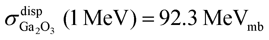 . This is useful for comparing effects of neutron irradiation with differing fluences and energy spectra. The calculation of neutron displacement damage dose can be used to develop a damage effect correlation for other radiation particle types based on the displacement damage dose.
 | ||
| Fig. 8 Group-wise displacement damage cross sections for neutron irradiation of Ga2O3. Reprinted with permission from Chaiken and Blue,58 copyright 2018, IEEE. | ||
(ii) Fast ion damage
The anisotropic expansion and amorphization of Ga2O3 irradiated with 946 MeV Au ions was examined.38 Damage saturation below amorphisation in ion implanted β-Ga2O3 using P, Ar and Sn ions with ion fluences from 1011–2 × 1015 cm−2 has also been reported.53 The concentration of displaced lattice atoms increased with ion fluence up to a saturation value of 90%. Further implantation only led to a broadening of the distribution, while the concentration remained at 90%. The ion fluence dependence of maximum damage concentration was modelled assuming the presence of point defects (which can recombine with those already existing from previous ion impacts) and non-recombinable damage clusters.53 The damage predominantly consisted of randomly displaced lattice atoms, i.e. point defects and their complexes. For higher damage levels, there was also a contribution from correlated displaced lattice atoms, suggesting the damage clusters are not amorphous.53(iii) Proton damage in Ga2O3 nanobelt transistors
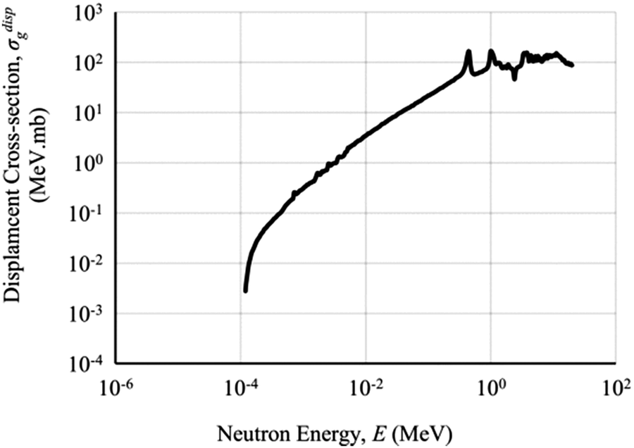
Proton damage in back-gated field-effect transistors (FETs) fabricated on exfoliated β-Ga2O3 nano-layers (nanobelts) was studied for fluences of 10 MeV protons.18 The radiation damaged FETs showed a decrease of 73% in the field-effect mobility and a positive shift of threshold voltage after proton irradiation at 2 × 1015 cm−2, which corresponds to approximately 105 times the intensity of a solar proton event. The on/off ratio of the FETs was maintained even after proton doses of 2 × 1015 cm−2. The data are summarized in the drain–source characteristics of Fig. 9, which show the effect of proton dose.18 Doses of 1–2 × 1015 cm−2 both lead to significant suppression of drain current. The radiation-induced damage in β-Ga2O3-based FETs was significantly recovered after annealing at 500 °C. This temperature is similar to that needed for removal of plasma-induced dry etch damage in Ga2O3.59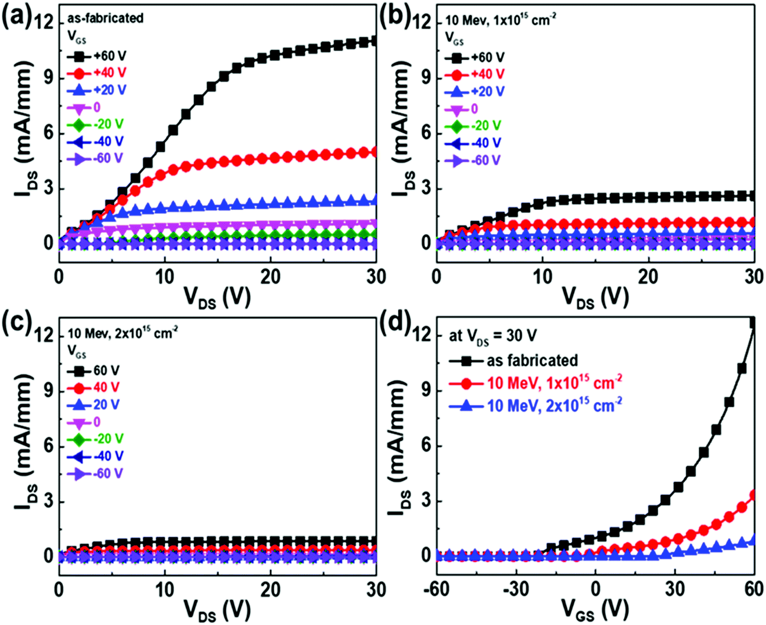 | ||
| Fig. 9 Output characteristics (IDSvs. VDS) of β-Ga2O3 nanobelt FET before and after 10 MeV proton irradiation at different doses: (a) as-fabricated, (b) 1 × 1015 cm−2, and (c) 2 × 1015 cm−2, and (d) transfer characteristics (IDSvs. VGS) of β-Ga2O3 nanobelt FET at VDS = 30 V before and after 10 MeV proton irradiation at different doses. Reprinted with permission from Yang et al.,18 copyright 2017, American Chemical Society. | ||
(iv) Proton damage in Ga2O3 rectifiers
10 MeV proton irradiation of vertical geometry Ga2O3 rectifiers at a fixed fluence of 1014 cm−2 produced trap states that reduced the carrier concentration in the Ga2O3, with a carrier removal rate of 235.7 cm−1 for protons of this energy.60Fig. 10 shows the reverse I–V characteristics before and after irradiation and subsequent annealing, as well as the corresponding capacitance–voltage data used to extract carrier loss rates. Annealing at 300 °C produced a recovery of approximately half of the carriers in the Ga2O3, while annealing at 450 °C almost restored the reverse breakdown voltage.60 The on/off ratio of the rectifiers was severely degraded by proton damage and was only partially recovered by 450 °C annealing. The minority carrier diffusion length decreased from ∼340 nm in the starting material to ∼315 nm after proton irradiation.61,62 The reverse recovery characteristics showed little change, with values in the range 20–30 ns before and after proton irradiation.63 | ||
| Fig. 10 Reverse current density–voltage characteristics from rectifiers before and after 10 MeV proton irradiation with a fluence of 1014 and then annealed at either 300 or 450 °C (top). C−2–V characteristics of Ga2O3 rectifiers before and after proton irradiation and subsequent annealing at either 300 or 450 °C (bottom). Reprinted with permission from Yang et al.,60 copyright 2108, American Institute of Physics. | ||
(v) Trap states induced by proton irradiation
Fig. 11 shows a compilation of trap states observed in as-grown and proton-irradiated Ga2O3. These states span a large portion of the gap.61,64–66Table 2 shows a summary of the trap parameters and possible origin of these states. The trap assignations are still tentative in most cases.61,64–66 | ||
| Fig. 11 Schematic of energy levels in the gap of as-grown and proton irradiated Ga2O3. | ||
| Trap notation | E a (eV) | σ n or σp (cm2) | Material or method | Induced by irradiation | Possible identity |
|---|---|---|---|---|---|
| α p calculated from an ODLTS Arrhenius plot assuming a hole effective mass equal to 1. LCV is CV characteristics with monochromatic light excitation, SSPC is steady state photocapacitance, ODLTS is deep level transient spectroscopy with optical excitation, DLOS is deep level optical spectroscopy. | |||||
| E178 | 0.55–0.62 | (3–30) × 10−14 | Bulk Sn doped,78 bulk Si doped,64 HVPE Si doped61 | 10–20 MeV protons, 18 MeV α-particles | Unknown |
| E278 | 0.74–0.82 | (3–30) × 10−16 | Bulk Sn doped,78 bulk Si doped,64 HVPE Si doped,61,66 MBE Ge doped,79 FETs80 | — | Fe61,78,80 |
| E2*66 | 0.75–0.79 | (3–7) × 10−14 | HVPE Si doped,61,66 FETs80 | 0.8 MeV protons, 10 MeV protons, 20 MeV protons, 18 MeV α-particles | Native defect complex |
| E378 | 0.95–1 | (0.6–6) × 1013 | Bulk Sn doped,78 bulk Si doped,64 HVPE Si doped,61,66 MBE Ge doped79 | 10–20 MeV protons, 18 MeV α-particles | Unknown |
| E461 | 1.2 | (4–15) × 10−14 | 10–20 MeV protons, 18 MeV α-particles | VO(III) | |
| E5 | 0.18 | (1–7) × 10−19 | MBE Ge doped79 | — | Unknown |
| E6 | 0.21 | (0.2–2) × 10−15 | MBE Ge doped, MOCVD Sn doped52 | — | Unknown |
| E761,66 | 0.27–0.29 | 5.6 × 10⁻¹⁸ | HVPE Si doped | 20 MeV protons, 18 MeV α-particles | Unknown |
| H1(STH)81 | 0.2–0.3 | (2.3–14) × 10−15 | ODLTS81 | HVPE Si doped as-grown, HVPE Si doped and irradiated with 20 MeV protons or 18 MeV α-particles | Self-trapped holes81 |
| H3 | 1.3–1.4 | 2.9 × 10⁻¹² | ODLTS, LCV, SSPC81 | HVPE Si doped as grown, HVPE Si doped as grown and irradiated with 20 MeV protons and 18 MeV α-particles, MOCVD Sn doped | VGa |
| H4 | DLOS,64,79 LCV, SSPC52,61,81 | Bulk Si doped, MBE Ge doped, MOCV Sn doped, neutron irradiated, 10–20 MeV proton irradiated, 18 MeV α-particles | Unknown | ||
| H5 | DLOS,79 LCV, SSPC52,61,81 | MBE Ge doped | Possibly same as H381 | ||
| H6 | DLOS64,79 | Bulk Si doped, MBE Ge doped, neutron irradiated | Possibly same as H1(STH) | ||
| H7 | DLOS79 | MBE Ge doped | Possibly same as E2*61,81 | ||
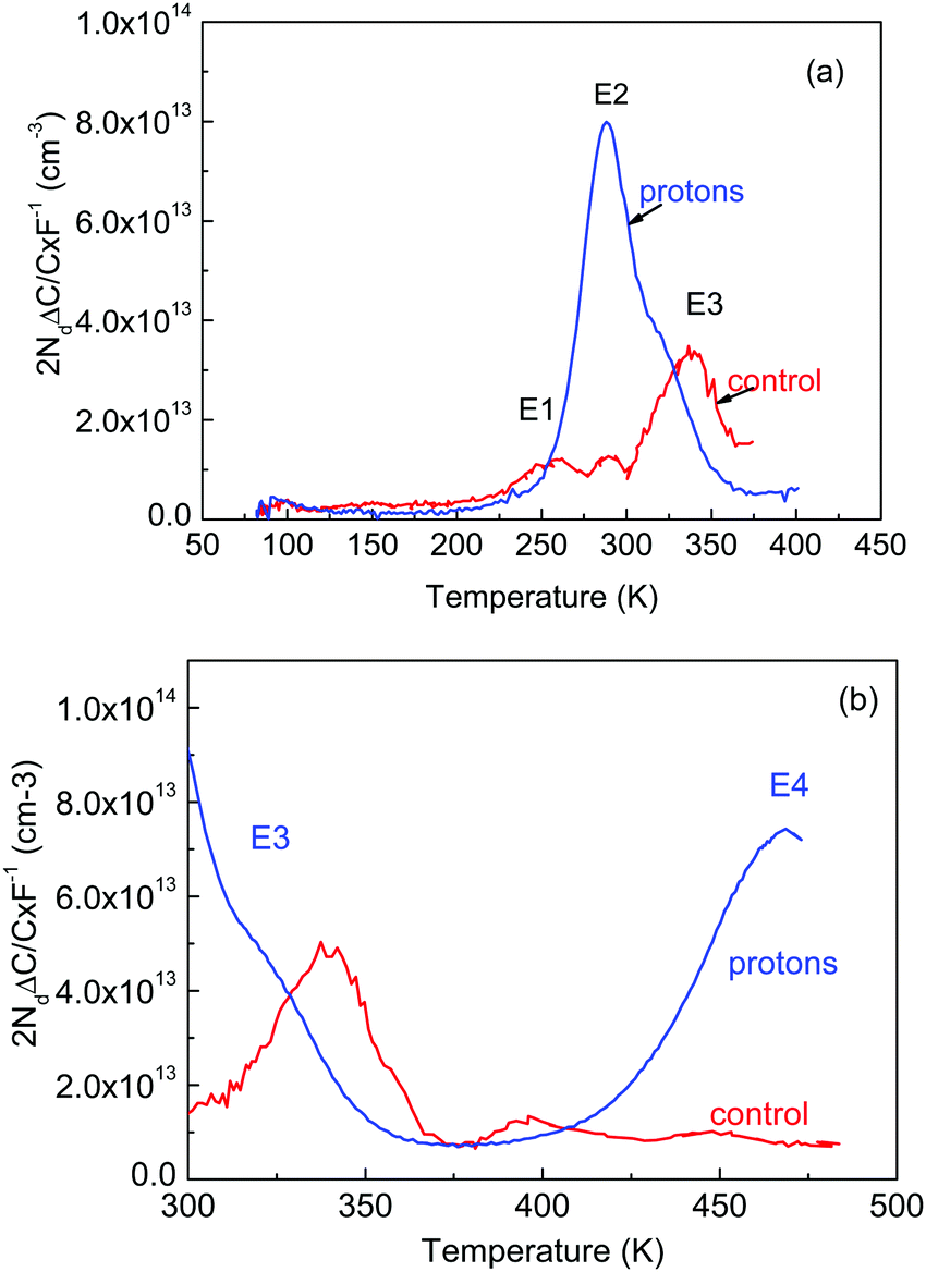
Epitaxial films of β-Ga2O3 grown by hydride vapor phase epitaxy (HVPE) on native substrates exhibit deep electron traps near Ec-0.6 eV, Ec-0.75 eV, and Ec-1.05 eV, similar to the E1, E2, and E3 electron traps observed in bulk β-Ga2O3 crystals.61,64–66 The concentration of these traps in the HVPE films is 1–2 orders of magnitude lower than in the bulk material.61 Proton irradiation increased the density of E2 (Ec-0.75 eV) and Ec-2.3 eV traps, suggesting these incorporate native defects. Irradiation with 10–20 MeV protons creates deep electron and hole traps, a strong increase in photocapacitance and prominent persistent photocapacitance that partly persists above room temperature.61,62 Typical DLTS spectra from samples before and after 10 MeV proton irradiation are shown in Fig. 12, with the presence of a prominent electron trap near Ec-1.05 eV (a capture cross section of σn = 2 × 10⁻¹² cm2) in the control sample. Two minor traps with levels Ec-0.6 eV (σn = 5.6 × 10⁻¹⁵ cm2) and Ec-0.75 eV (σn = 6.5 × 10⁻¹⁵ cm2) were also detected. After proton irradiation, the dominant peak in DLTS spectra was an electron trap with level Ec-0.75 eV (electron capture cross section σn = 6.5 × 10⁻¹⁵ cm2), with a prominent shoulder due to the Ec-1.05 eV electron trap. In the notation of ref. 64, these are respectively E1, E2, and E3 electron traps. The concentrations of E2 and E3 increased and a new trap E4 at Ec-1.2 eV emerged after proton irradiation. Fig. 13 shows the variation of DLTS (top) and ODLTS (bottom) peak amplitude and shape as a function of rate window for samples irradiated with 20 MeV protons.
 | ||
| Fig. 12 (a) DLTS spectra for β-Ga2O3 epilayers and (b) high temperature DLTS spectra, before (red line) and after (blue line) proton irradiation. Reprinted with permission from Polyakov et al.,61 copyright 2018, American Institute of Physics. | ||
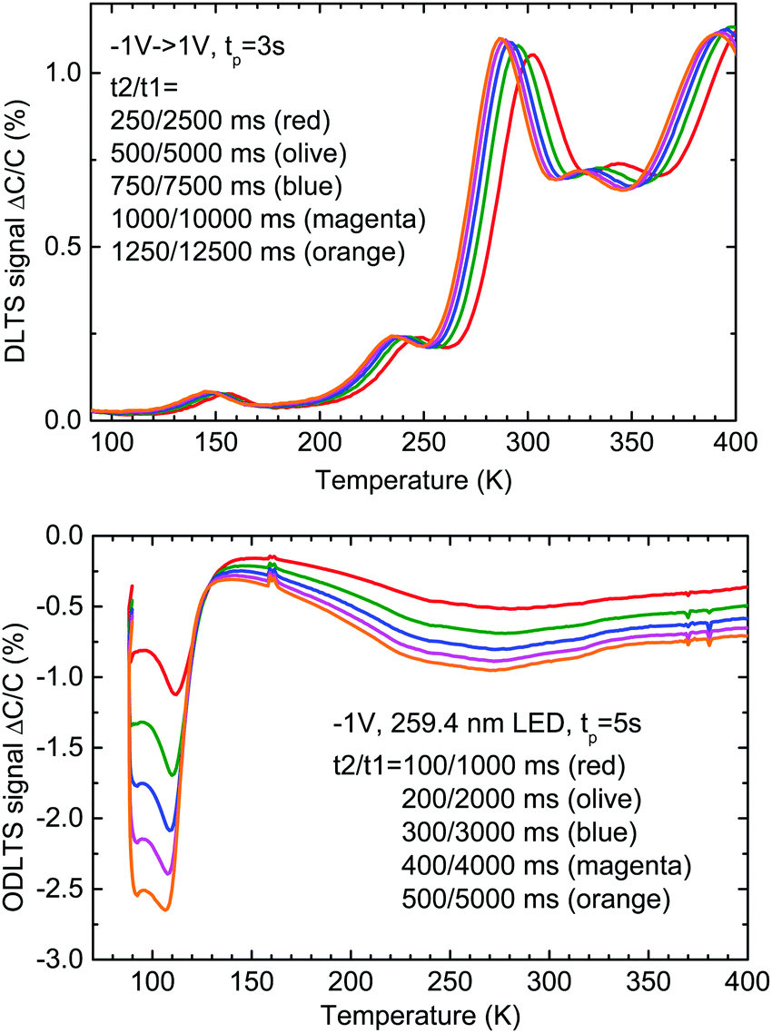 | ||
| Fig. 13 (top) DLTS spectra of Ga2O3 rectifiers after 20 MeV proton irradiation with a fluence of 1014 cm−2, bias −1 V, pulse +1 V, tp = 3 s, showing variation of electron trap peaks with different rate windows; (bottom) ODLTS spectra after irradiation with fluence 1014 cm−2, bias −1 V, 259.4 nm LED, tp = 5 s, showing variation of the hole trap signal with rate window settings. | ||
Hole traps in the lower half of the bandgap were investigated using optical injection. Three hole-traps H1 (STH), H2 (ECB) and H3, with activation energies 0.2, 0.4, and 1.3 eV, respectively, were detected. The H1 (STH) feature was suggested to correspond to the transition of polaronic states of self-trapped holes (STH) to mobile holes in the valence band. The broad H2 (ECB) feature was assigned to overcoming of the electron capture barrier (ECB) of centers responsible for persistent photocapacitance at T < 250 K. The H3 peak was produced by detrapping of holes from Ev + (1.3–1.4) eV hole traps related to VGa acceptors. A deep acceptor with an optical ionization threshold near 2.3 eV is likely responsible for high temperature persistent photocapacitance surviving up to temperatures higher than 400 K. Table 2 summarizes reported trap state energy levels, capture cross sections and possible origin in as-grown and irradiated Ga2O3.
(vi) Dominant defect induced by proton irradiation
There is particular interest in the properties of hydrogen in Ga2O3 because of the predictions from density functional theory and total energy calculations that it should be a shallow donor in this material.34,67 The generally observed n-type conductivity, therefore, may at least in part be explained by the presence of residual hydrogen from the growth ambient, rather than to native defects such as Ga interstitials or O vacancies, the latter of which are suggested to be deep donors.67–70 There is some experimental support for the fact that hydrogen may be a shallow donor in Ga2O3 from experiments on its muonium counterpart and from electron paramagnetic resonance of single-crystal samples.68Fourier transform infrared spectroscopy studies on samples ion implanted with hydrogen or deuterium to obtain concentrations of ∼1020 cm−3 were used to examine temperature- and polarization-dependent effects as well as relative H- and D-concentrations.71 These results, coupled with detailed theoretical calculations, showed no evidence of interstitial atomic hydrogen (Hi); instead, the defects observed involve H trapped at a Ga vacancy, the primary member involving a particular two-H configuration. This configuration is shown in Fig. 14.71 The dominant hydrogen or deuterium absorption lines appear at 3437 and 2545 cm−1, respectively. Incorporation of H2 and D2 simultaneously, splits these OH and OD lines into two lines. This requires the defects contain two equivalent H atoms. This, and the fact that the lines are completely polarized, leads to the model where two H atoms are bonded to a Ga vacancy. When the samples are implanted with hydrogen, additional absorption peaks are observed. As they are annealed, these defects become converted into the 3437 and 2545 cm−1 lines at 400 °C. These lines are stable up to 700 °C, where they are then converted into other new lines.71
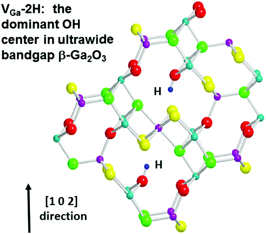 | ||
| Fig. 14 Schematic of the VGa-2H defect in proton irradiated Ga2O3. Reprinted with permission from Weiser et al.,71 copyright 2018, American Institute of Physics. | ||
(vii) Electron irradiation damage
1.5 MeV electron irradiation of vertical rectifiers fabricated on epi Ga2O3 on bulk β-Ga2O3 at fluences from 1.79 × 10¹⁵ to 1.43 × 1016 cm−2 caused a reduction in carrier concentration in the Ga2O3, with a carrier removal rate of 4.9 cm−1.72–74 This compares to a carrier removal rate of ∼300 cm−1 for 10 MeV protons in the same material. Fig. 15 (top) shows the 2 kT region of the forward current–voltage characteristics increased due to electron-induced damage, with a more than 2 orders of magnitude increase in on-state resistance at the highest fluence.72 There was a reduction in reverse current, which scaled with electron fluence. The on/off ratio at −10 V reverse bias voltage was severely degraded by electron irradiation, decreasing from approximately 107 in the un-irradiated reference diodes to approximately 2 × 10⁴ for the highest fluence of 1.43 × 1016 cm−2. The changes in device characteristics were accompanied by a decrease in electron diffusion length from 325 to 240 μm at 300 K,74 as shown at the bottom of Fig. 15. Time-resolved cathodoluminescence after 1.5 MeV electron irradiation showed a 210 ps decay lifetime and reduction in carrier lifetime with increased fluence.74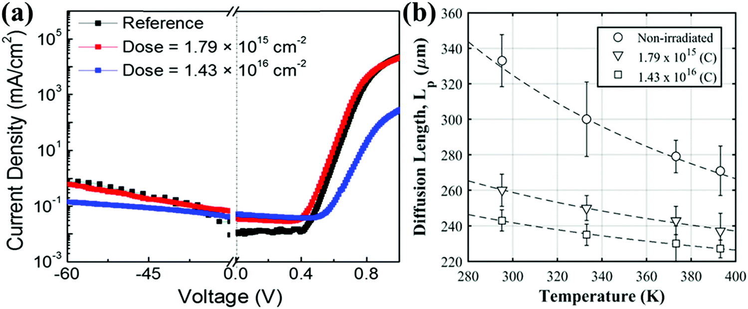 | ||
| Fig. 15 (a) I–Vs from Ga2O3 diodes before and after 1.5 MeV electron irradiation of different doses and (b) diffusion length of electrons as a function of temperature after different electron irradiation doses. Reprinted with permission from Yang et al.,72 copyright 2018, American Institute of Physics. | ||
(viii) Alpha particle damage
Ga2O3 rectifiers irradiated with 18 MeV alpha particles with fluences of 1012–1013 cm−2, simulating space radiation exposure,75 exhibited carrier removal rates in the drift region of 406–728 cm−1. These values are factors of 2–3 higher than for high energy (10 MeV) protons and two orders of magnitude higher than for 1.5 MeV electron irradiation of the same material. The reverse breakdown voltage increased in response to a reduction in channel carrier density (Fig. 16) and the on/off ratio was also degraded. The on-state resistance of the rectifiers was more degraded by alpha particle irradiation than either ideality factor or barrier height.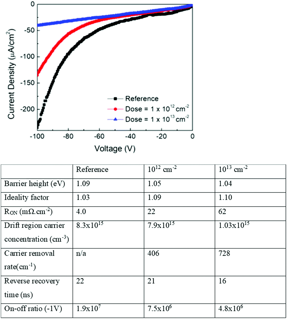 | ||
| Fig. 16 Reverse I–Vs from Ga2O3 rectifiers before and after 18 MeV alpha particle damage, along with summary of changes in device properties. Reprinted with permission from Yang et al.,75 copyright 2018, American Institute of Physics. | ||
(ix) γ-Ray damage
Wong et al.76 examined the gamma-ray irradiation tolerance of lateral depletion mode β-Ga2O3 MOSFETs to doses of 1.6 MGray (SiO2), with little effect on output current and threshold voltage of this total dose. A dose of 1 Gray (Gy) corresponds to an absorbed radiation energy of 1 J per kg of mass, with SiO2 being a common reference material. Degradation in the gate oxide was found to limit the overall radiation resistance.76(x) X-Ray damage
Constant voltage stress of β-Ga2O3 MOS capacitors with Al2O3 gate dielectrics showed increasing electron-trap densities for increasingly positive stress voltages, and hole traps created for irradiation with 10 keV X-rays devices at a dose rate of 31.5 krad (SiO2) min−1 under grounded bias conditions.77 Stress-induced traps were located primarily in the Al2O3 gate dielectric layer, and distributed broadly in energy. Oxygen vacancies in the Al2O3 were suggested to be the most likely defects created.77 The radiation-induced voltage shifts were comparable to or less than those of the MOSFETs exposed to gamma-rays discussed above.76Fig. 17 shows a compilation of carrier removal rates in Ga2O3 for different types and energy of radiation. The data reported to date show that the carrier removal rates in Ga2O3 are basically comparable to those reported previously for GaN.31–33,35,36
 | ||
| Fig. 17 Carrier removal rate in Ga2O3 as a function of energy for different types of radiation. Data is either from University of Florida (UF),60,72,75 National University of Science and Technology (UST-MISiS) or Ohio State University (OSU).55,56 | ||
Conclusions
The present review has comprehensively examined the radiation hardness of a promising ultra-wide bandgap material, β-Ga2O3. Therefore, the radiation damage by high energy particles was investigated at both material and device levels. The initial data on proton, electron, X-ray, gamma and neutron irradiation of β-Ga2O3 show fairly comparable radiation resistance to conventional wide bandgap semiconductors under similar conditions. The carrier removal rates in irradiated rectifier structures range from ∼5 cm−1 for 1.5 MeV electrons to 730 cm−1 for 18 MeV alpha particles. Thermal annealing at ∼500 °C brings a significant recovery towards the initial, un-irradiated characteristics. The dominant defect formed in Ga2O3 by annealing in an H2 ambient or by the implantation of protons is a specific relaxed VGa-2H structure corresponding to the 3437 cm−1 line that dominates the infrared absorption spectra. There is significant scope for additional work to determine carrier removal rates at additional energies for each radiation type, and to look for dose-rate effects, SEU responses, the role of interfaces in MOS structures and annealing stages of the induced defects. In the latter case, it is of importance to know whether in situ thermal annealing or forward biased minority carrier injection annealing are effective in Ga2O3 devices, since these could be used as simple refresh cycles for radiation damaged devices.Conflicts of interest
There are no conflicts to declare.Acknowledgements
The work at Korea University was supported by Space Core Technology Development Program (2017M1A3A3A02015033) and the Technology Development Program to Solve Climate Changes (2017M1A2A2087351) through the National Research Foundation of Korea funded by the Ministry of Science, ICT and Future Planning of Korea. The work at UF is partially supported by HDTRA1-17-1-0011 (Jacob Calkins, monitor). The project or effort depicted is sponsored by the Department of the Defense, Defense Threat Reduction Agency. The content of the information does not necessarily reflect the position or the policy of the federal government, and no official endorsement should be inferred. The work at NUST MISiS was supported in part by the Ministry of Education and Science of the Russian Federation in the framework of Increase Competitiveness Program of NUST (MISiS) (K2-2014-055).References
- J. Y. Tsao, S. Chowdhury, M. A. Hollis, D. Jena, N. M. Johnson, K. A. Jones, R. J. Kaplar, S. Rajan, C. G. Van de Walle, E. Bellotti, C. L. Chua, R. Collazo, M. E. Coltrin, J. A. Cooper, K. R. Evans, S. Graham, T. A. Grotjohn, E. R. Heller, M. Higashiwaki, M. S. Islam, P. W. Juodawlkis, M. A. Khan, A. D. Koehler, J. H. Leach, U. K. Mishra, R. J. Nemanich, R. C. N. Pilawa-Podgurski, J. B. Shealy, M. J. Tadjer, A. F. Witulski, M. Wraback and J. A. Simmons, Adv. Electron. Mater., 2018, 4, 1600501, DOI:10.1002/aelm.201600501.
- A. Kuramata, K. Koshi, S. Watanabe, Y. Yamaoka, T. Masui and S. Yamakoshi, Jpn. J. Appl. Phys., 2016, 55, 1202A2 CrossRef.
- H. V. Wenckstern, Adv. Electron. Mater., 2017, 3, 1600350 CrossRef.
- M. A. Mastro, A. Kuramata, J. Calkins, J. Kim, F. Ren and S. J. Pearton, ECS J. Solid State Sci. Technol., 2017, 6, P356 CrossRef CAS.
- M. J. Tadjer, M. A. Mastro, N. A. Mahadik, M. Currie, V. D. Wheeler, J. A. Freitas, Jr., J. D. Greenlee, J. K. Hite, K. D. Hobart, C. R. Eddy, Jr. and F. J. Kub, J. Electron. Mater., 2016, 45, 2031 CrossRef CAS.
- B. Bayraktaroglu, Assessment of Ga2O3 Technology, Air Force Research Lab, Devices for Sensing Branch, Aerospace Components & Subsystems Division, Report AFRL-RY-WP-TR-2017-0167, 2017, http://www.dtic.mil/dtic/tr/fulltext/u2/1038137.pdf.
- S. I. Stepanov, V. I. Nikolaev, V. E. Bougrov and A. E. Romanov, Rev. Adv. Mater. Sci., 2016, 44, 63 CAS.
- S. Rafique, L. Han and H. Zhao, ECS Trans., 2017, 80, 203 CrossRef CAS.
- S. J. Pearton, J. Yang, P. H. Cary IV, F. Ren, J. Kim, M. J. Tadjer and M. A. Mastro, Appl. Phys. Rev., 2018, 5, 011301 Search PubMed.
- M. Higashiwaki and G. H. Jessen, Appl. Phys. Lett., 2018, 112, 060401, DOI:10.1063/1.5017845.
- A. M. Armstrong, M. H. Crawford, A. Jayawardena, A. Ahyi and S. Dhar, J. Appl. Phys., 2016, 119, 103102 CrossRef.
- J. Kim, S. Oh, M. A. Mastro and J. Kim, Phys. Chem. Chem. Phys., 2016, 18, 15760 RSC.
- M. Kim, J.-H. Seo, U. Singisetti and Z. Ma, J. Mater. Chem. C, 2017, 5, 8338 RSC.
- D. Gogova, G. Wagner, M. Baldini, M. Schmidbauer, K. Irmscher, R. Schewski, Z. Galazka, M. Albrecht and R. Fornari, J. Cryst. Growth, 2014, 401, 665 CrossRef CAS.
- D. Gogova, M. Schmidbauer and A. Kwasniewski, CrystEngComm, 2015, 17, 6744 RSC.
- E. Chikoidze, A. Fellous, A. Perez-Tomas, G. Sauthier, T. Tchelidze, C. Ton-That, T. T. Huynh, M. Phillips, S. Russell, M. Jennings, B. Berini, F. Jomard and Y. Dumont, Mater. Today Phys., 2017, 3, 118 CrossRef.
- J. Kim, M. A. Mastro, M. J. Tadjer and J. Kim, ACS Appl. Mater. Interfaces, 2017, 9, 21322 CrossRef CAS.
- G. Yang, S. Jang, F. Ren, S. J. Pearton and J. Kim, ACS Appl. Mater. Interfaces, 2017, 9, 40471 CrossRef CAS.
- Z. Galazka, R. Uecker, D. Klimm, K. Irmscher, M. Naumann, M. Pietsch, A. Kwasniewski, R. Bertram, S. Ganschow and M. Bickermann, ECS J. Solid State Sci. Technol., 2017, 6, Q3007 CrossRef CAS.
- M. Baldini, M. Albrecht, A. Fiedler, K. Irmscher, R. Schewski and G. Wagner, ECS J. Solid State Sci. Technol., 2017, 6, Q3040 CrossRef CAS.
- S. Rafique, L. Han, M. J. Tadjer, J. A. Freitas Jr, N. A. Mahadik and H. Zhao, Appl. Phys. Lett., 2016, 108, 182105 CrossRef.
- J. F. Ziegler and W. A. Lanford, Science, 1979, 206, 776 CrossRef CAS.
- J. S. Melinger, S. Buchner, D. McMorrow, W. J. Stapor, T. R. Weatherford, A. B. Campbell and H. Eisen, IEEE Trans. Nucl. Sci., 1994, 41, 2574, DOI:10.1109/23.340618.
- E. Normand, IEEE Trans. Nucl. Sci., 1996, 43, 461, DOI:10.1109/23.490893.
- S. Duzellier, Aerosp. Sci. Technol., 2005, 9, 93, DOI:10.1016/j.ast.2004.08.006.
- F. W. Sexton, IEEE Trans. Nucl. Sci., 2003, 50, 603, DOI:10.1109/TNS.2003.813137.
- E. Petersen, Single Event Effects in Aerospace, John Wiley & Sons, NY, 2011 Search PubMed.
- J. F. Ziegler, M. D. Ziegler and J. P. Biersack, Nucl. Instrum. Methods Phys. Res., Sect. B, 2010, 268, 1818 CrossRef CAS.
- J. R. Srour and J. W. Palko, IEEE Trans. Nucl. Sci., 2006, 53, 3610 CrossRef CAS.
- J. Nord, K. Nordlund and J. Keinonen, Phys. Rev. B: Condens. Matter Mater. Phys., 2003, 68, 184104 CrossRef.
- S. J. Pearton, Y.-S. Hwang and F. Ren, J. Mater., 2015, 67, 1601 CAS.
- A. Ionascut-Nedelcescu, C. Carlone, A. Houdayer, H. J. von Bardeleben, J.-L. Cantin and S. Raymond, IEEE Trans. Nucl. Sci., 2002, 49, 2733 CrossRef CAS.
- B. D. Weaver, T. J. Anderson, A. D. Koehler, J. D. Greenlee, J. K. Hite, D. I. Shahin, F. J. Kub and K. D. Hobart, ECS J. Solid State Sci. Technol., 2016, 5, Q208 CrossRef CAS.
- J. B. Varley, J. R. Weber, A. Janotti and C. G. Van de Walle, Appl. Phys. Lett., 2010, 97, 142106 CrossRef.
- A. Y. Polyakov, S. J. Pearton, P. Frenzer, F. Ren, L. Liu and J. Kim, J. Mater. Chem. C, 2013, 1, 877 RSC.
- S. J. Pearton, R. Deist, F. Ren, L. Liu, A. Y. Polyakov and J. Kim, J. Vac. Sci. Technol., A, 2013, 31, 050801 CrossRef.
- L. N. Cojocaru, Radiat. Eff., 1974, 21, 157, DOI:10.1080/00337577408241456.
- C. L. Tracy, M. Lang, D. Severin, M. Bender, C. Trautmann and R. C. Ewing, Nucl. Instrum. Methods Phys. Res., Sect. B, 2016, 374, 40 CrossRef CAS.
- See the extensive database of The NASA Goddard Space Flight Center Radiation Effects effort, https://radhome.gsfc.nasa.gov/.
- E. G. Stassinopoulos, G. J. Brucker, D. W. Nakamura, C. A. Stauffer, G. B. Gee and J. L. Barth, IEEE Trans. Nucl. Sci., 1996, 43, 369 CrossRef.
- M. J. Campola, D. J. Cochran, S. Alt, A. J. Boutte, D. Chen, R. A. Gigliuto, K. A. LaBel, J. A. Pellish, R. L. Ladbury, M. C. Casey, E. P. Wilcox, M. V. O'Bryan, J.-M. Lauenstein and M. A. Xapsos, Compendium of Total Ionizing Dose and Displacement Damage Results from NASA Goddard Spaceflight Center, 2016 IEEE Radiation Effects Data Workshop (REDW), Portland, Oregon 11–15 July 2016, pp. 1–9, ISBN: 978-1-5090-5114-4.
- T. R. Oldham, K. W. Bennett, J. Beaucour, T. Carriere, C. Polvey and P. Garnier, IEEE Trans. Nucl. Sci., 1993, 40, 1820 CrossRef CAS.
- P. E. Dodd, F. W. Sexton and P. S. Winokur, IEEE Trans. Nucl. Sci., 1994, 41, 2005 CAS.
- L. Scheick, IEEE Trans. Nucl. Sci., 2014, 61, 2881 CAS.
- A. P. Karmarkar, B. D. White, D. Buttari, D. M. Fleetwood, R. D. Schrimpf, R. A. Weller, L. J. Brillson and U. K. Mishra, IEEE Trans. Nucl. Sci., 2005, 52, 2239 CAS.
- S. J. Pearton, F. Ren, E. Patrick, M. E. Law and A. Y. Polyakov, ECS J. Solid State Sci. Technol., 2016, 5, Q35 CrossRef CAS.
- Courtesy of Jacob Calkins, Defense Threat Reduction Agency, http://www.dtra.mil/Research/Basic-and-Applied-Science/.
- E. Korhonen, F. Tuomisto, D. Gogova, G. Wagner, M. Baldini, Z. Galazka, R. Schewski and M. Albrecht, Appl. Phys. Lett., 2015, 106, 242103 CrossRef.
- B. E. Kananen, L. E. Halliburton, K. T. Stevens, G. K. Foundos, K. B. Chang and N. C. Giles, Appl. Phys. Lett., 2017, 110, 202104 CrossRef.
- B. E. Kananen, N. C. Giles, L. E. Halliburton, G. K. Foundos, K. B. Chang and K. T. Stevens, J. Appl. Phys., 2017, 122, 215703, DOI:10.1063/1.5007095.
- A. Kyrtsos, M. Matsubara and E. Bellotti, Phys. Rev. B, 2017, 95, 245202, DOI:10.1103/PhysRevB.95.245202.
- A. Y. Polyakov, N. B. Smirnov, I. V. Shchemerov, D. Gogova, S. A. Tarelkin and S. J. Pearton, J. Appl. Phys., 2018, 123, 115702 CrossRef.
- E. Wendler, E. Treiber, J. Baldauf, S. Wolf and C. Ronnig, Nucl. Instrum. Methods Phys. Res., Sect. B, 2016, 379, 85 CrossRef CAS.
- L. Dong, R. Jia, C. Li, B. Xin and Y. Zhang, J. Alloys Compd., 2017, 712, 379, DOI:10.1016/j.jallcom.2017.04.020.
- A. A. Arehart, E. Farzana, T. E. Blue and S. A. Ringel, presented at 2nd International Workshop on Ga2O3 and Related Materials, Parma, Italy, September 2017.
- S. Ringel, et al., The presence and impact of deep level defects induced by high energy neutron radiation in beta-phase gallium oxide, GOMACTech, 2018 Search PubMed.
- D. Szalkai, Z. Galazka, K. Irmscher, P. Tüttő, A. Klix and D. Gehre, IEEE Trans. Nucl. Sci., 2017, 64, 1574 CAS.
- M. F. Chaiken and T. E. Blue, IEEE Trans. Nucl. Sci., 2018, 65, 1147 Search PubMed.
- J. Yang, F. Ren, R. Khanna, K. Bevlin, D. Geerpuram, L.-C. Tung, J. Lin, H. X. Jiang, J. Lee, E. Flitsiyan, L. Chernyak, S. J. Pearton and A. Kuramata, J. Vac. Sci. Technol., B: Nanotechnol. Microelectron.: Mater., Process., Meas., Phenom., 2017, 35, 051201 Search PubMed.
- J. Yang, Z. Chen, F. Ren, S. J. Pearton, G. Yang, J. Kim, J. Lee, E. Flitsiyan, L. Chernyak and A. Kuramata, J. Vac. Sci. Technol., B: Nanotechnol. Microelectron.: Mater., Process., Meas., Phenom., 2018, 36, 011206 Search PubMed.
- A. Y. Polyakov, N. B. Smirnov, I. V. Shchemerov, E. B. Yakimov, J. Yang, F. Ren, G. Yang, J. Kim, A. Kuramata and S. J. Pearton, Appl. Phys. Lett., 2018, 112, 032107 CrossRef.
- E. B. Yakimov, A. Y. Polyakov, N. B. Smirnov, I. V. Shchemerov, J. Yang, F. Ren, G. Yang, J. Kim and S. J. Pearton, J. Appl. Phys., 2018, 123, 185704 CrossRef.
- S. Ahn, Y.-H. Lin, F. Ren, S. Oh, Y. Jung, G. Yang, J. Kim, M. A. Mastro, J. K. Hite, C. R. Eddy, Jr. and S. J. Pearton, J. Vac. Sci. Technol., B: Nanotechnol. Microelectron.: Mater., Process., Meas., Phenom., 2016, 34, 041213 Search PubMed.
- Z. Zhang, E. Farzana, A. R. Arehart and S. A. Ringel, Appl. Phys. Lett., 2016, 108, 052105, DOI:10.1063/1.4941429.
- Y. Nakano, ECS J. Solid State Sci. Technol., 2017, 6, P615 CrossRef CAS.
- M. E. Ingebrigtsen, J. B. Varley, A. Yu. Kuznetsov, B. G. Svensson, G. Alfieri, A. Mihaila, U. Badstübner and L. Vines, Appl. Phys. Lett., 2018, 112, 042104, DOI:10.1063/1.5020134.
- A. Janotti and C. G. Van de Walle, Nat. Mater., 2007, 6, 44 CrossRef CAS.
- P. D. C. King and T. D. Veal, J. Phys.: Condens. Matter, 2011, 23, 334214 CrossRef CAS.
- S. Ahn, F. Ren, E. Patrick, M. E. Law, S. J. Pearton and A. Kuramata, Appl. Phys. Lett., 2016, 109, 242108 CrossRef.
- S. Ahn, F. Ren, E. Patrick, M. E. Law and S. J. Pearton, ECS J. Solid State Sci. Technol., 2017, 6, Q3026 CrossRef CAS.
- P. Weiser, M. Stavola, W. Beall Fowler, Y. Qin and S. J. Pearton, Appl. Phys. Lett., 2018, 112, 232104 CrossRef.
- J. Yang, F. Ren, S. J. Pearton, G. Yang, J. Kim and A. Kuramata, J. Vac. Sci. Technol., B: Nanotechnol. Microelectron.: Mater., Process., Meas., Phenom., 2017, 35, 031208 Search PubMed.
- J. Lee, E. Flitsiyan, L. Chernyak, S. Ahn, F. Ren, L. Yun, S. J. Pearton, J. Kim, B. Meyler and J. Salzman, ECS J. Solid State Sci. Technol., 2017, 6, Q3049 CrossRef CAS.
- J. D. Lee, E. Flitsiyan, L. Chernyak, J. Yang, F. Ren, S. J. Pearton, B. Meyler and Y. J. Salzman, Appl. Phys. Lett., 2018, 112, 082104 CrossRef.
- J. Yang, C. Fares, Y. Guan, F. Ren, S. J. Pearton, J. Bae, J. Kim and A. Kuramata, J. Vac. Sci. Technol., B: Nanotechnol. Microelectron.: Mater., Process., Meas., Phenom., 2018, 36, 031205 Search PubMed.
- M. H. Wong, A. Takeyama, T. Makino, T. Ohshima, K. Sasaki, A. Kuramata, S. Yamakoshi and M. Higashiwaki, Appl. Phys. Lett., 2018, 112, 023503, DOI:10.1063/1.5017810.
- M. A. Bhuiyan, H. Zhou, R. Jiang, E. X. Zhang, D. M. Fleetwood, P. D. Ye and T.-P. Ma, IEEE Electron Device Lett., 2018, 39, 1022 Search PubMed.
- K. Irmscher, Z. Galazka, M. Pietsch, R. Uecker and R. Fornari, J. Appl. Phys., 2011, 110, 063720 CrossRef.
- E. Farzana, E. Ahmadi, J. S. Speck, A. R. Arehart and S. A. Ringel, J. Appl. Phys., 2018, 123, 161410 CrossRef.
- J. F. McGlone, Z. Xia, Y. Zhang, C. Joishi, S. Lodha, S. Rajan, S. A. Ringel and A. R. Arehart, IEEE Electron Device Lett., 2018, 39, 1042 Search PubMed.
- A. Y. Polyakov, N. B. Smirnov, I. V. Shchemerov, S. J. Pearton, F. Ren, A. V. Chernykh, P. B. Lagov and T. V. Kulevoy, APL Mater., 2018, 6, 096102 CrossRef.
| This journal is © The Royal Society of Chemistry 2019 |