
 Open Access Article
 This Open Access Article is licensed under a
 Creative Commons Attribution 3.0 Unported Licence
Earth abundant, non-toxic, 3D printed Cu2−xS with high thermoelectric figure of merit†
Matthew R.
Burton
 *a,
Shahin
Mehraban
b,
James
McGettrick
a,
Trystan
Watson
a,
Nicholas P.
Lavery
b and
Matthew J.
Carnie
*a
*a,
Shahin
Mehraban
b,
James
McGettrick
a,
Trystan
Watson
a,
Nicholas P.
Lavery
b and
Matthew J.
Carnie
*a
aSPECIFIC-IKC, Materials Research Centre, College of Engineering, Swansea University, Bay Campus, Fabian Way, Swansea, SA1 8EN, UK. E-mail: m.r.burton@swansea.ac.uk; m.j.carnie@swansea.ac.uk
bMACH1, Materials Research Centre, College of Engineering, Swansea University, Bay Campus, Fabian Way, Swansea, SA1 8EN, UK
First published on 29th October 2019
Abstract
The toxicity, earth abundance and manufacturing costs of thermoelectric materials are three leading reasons why thermoelectric generators are not used in wide scale applications. This is the first paper to tackle all three of these problems simultaneously. A pseudo-3D printing technique is combined with Cu2−xS based inks to yield bulk samples capable of being used in traditional architecture thermoelectric generators. These bulk samples are characterised over a wide temperature range in XPS, which reveals a curing temperature of 550 K yields pure Cu2−xS samples. The thermoelectric properties of these samples are tested over a wide temperature range, with a peak ZT of 0.63 ± 0.09 being recorded at 966 K. This work gives a significant advancement towards low cost highly efficient non-toxic thermoelectric generators. This work also provides the first route to print Cu2−xS, a material of much interest to the solar cell, catalysis and biosensor fields.
Introduction
Due to the diminishing supply of fossil fuels and the effects of climate change, the development of sustainable energy sources has become a necessity. Waste heat is of major concern, in the UK alone 48 TW h yr−1 of energy is lost from industry through heat.1 This accounts to around one sixth of all industrial energy and harvesting just 1% of this waste heat could equate to a 0.25 Tg year−1 reduction in CO2 emmissions.2 Thermoelectric generators offer a route of sustainable energy production, from this otherwise wasted heat energy. Thermoelectric generators could also power small electronic devices such as those required for the internet of things,3 and flexible generators have been shown to power wearable electronics.4 The efficiency of a thermoelectric material is related to the dimensionless figure of merit (ZT), which is comprised of the electrical conductivity (σ, S cm−1), the Seebeck coefficient (S, V K−1), the thermal conductivity (κ, W m−1 K−1) and the absolute temperature (T, K) as shown in eqn (1). A higher ZT correlates to a higher efficiency material.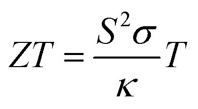 | (1) |
The most commonly used materials for thermoelectrics are Bi2Te3 and PbTe for room temperature and mid-temperature applications respectively. ZT was shown to be ∼1 in these materials in the 1950s.5,6 Although these materials have dominated thermoelectrics for some time, Te is a rare element with an Earth abundancy similar to that of Pt (1 μg kg−1).7 This along with the toxicity of Te, has prevented the wide scale use of thermoelectrics. Tin selenide (SnSe) has sparked much interest in the field of thermoelectrics, since the observation of the record ZT of 2.6 ± 0.3 at 923 K. Whilst the Earth abundancy of Se is fifty times greater than that of Te,7 Se abundance is still lower than Ag (75 μg kg−1) making Se a potentially costly constituent element. Additionally, the toxicity of Se makes the use of SnSe as a thermoelectric material far from ideal.8
In 2014 He et al. showed that Cu deficient copper(I) sulphide (Cu2S) exhibits a maximum ZT of 1.7 at 1000 K.9 The unique combination of all Earth abundant elements (Cu, 60 mg kg−1; S, 350 mg kg−1),7 non-toxic components and a high ZT has led to a large interest in this material in the thermoelectric community. In addition Cu2S is a material of much interest in solar cells,10–12 photocatalysis,13 catalysis14 and biosensors,15 due to Cu2S having a bulk band gap of 1.21 eV.16
Many fabrication techniques have been studied since Cu2S was discovered to be a highly efficient thermoelectric material, including melt-solidification,17 mechanochemical synthesis,18 ultrasonication and pressing,19 chemical synthesis and hot pressing,20 hydrothermal synthesis and hot pressing,21 hydrothermal synthesis and mechanical alloying followed by spark plasma sintering,22 mechanical alloying followed by spark plasma sintering,23 and mechanical alloying with Se doping followed by spark plasma sintering.24 These techniques however, require high pressure, high temperature and lengthy fabrication times which all contribute to the embodied energy of the material. In contrast, printing can be achieved at ambient temperature and pressure and with fast fabrication times. Printing of thermoelectrics has primarily focused on the production of films (∼300 μm), due to the limitations of printing techniques being studied for thermoelectrics, such as screen printing25,26 and inkjet printing.27 More recently printed elements that have dimensions of standard thermoelectric “legs” (i.e. not thin films) have been investigated for Bi2Te3 and SnSe with promising results.28,29 Whilst these examples show the potential of printed thermoelectrics, they both require toxic and low Earth abundant elements. This work for the first time demonstrates printed all Earth-abundant, standard geometry, thermoelectric elements.
Experimental
Ink formulation
Cu (99%, GoodFellow) and S (≥99.5%, Sigma Aldrich) powders were added in stoichiometric quantities to a 250 ml stainless steel grinding bowl (Fritsch), to which stainless steel ball bearings (30) of 10 mm in diameter were added. This was secured into a planetary mill (PULVERISETTE 5/2) and a sand filled grinding bowl was added as a counterbalance. This was set to spin (200 rpm for 30 minutes) followed by a resting period of 30 minutes, this cycle was repeated 60 times. Binder solutions were made by mixing sodium carboxymethylcellulose (average MW ∼250![[thin space (1/6-em)]](https://www.rsc.org/images/entities/char_2009.gif) 000, Sigma-Aldrich) with deionised water in a weight percentage of 4% in water. The binder mixing process was accelerated with the use of a centrifugal mixer (SpeedMixerTM DAC 150.1 FVZ). Binder solution (13 g) was mixed with ball milled powder (37 g) in a centrifugal mixer (1500 rpm for 60 seconds), the mixture was then briefly agitated on a vortex genie and stirred with a spatula. This process was repeated until a uniform paste was produced.
000, Sigma-Aldrich) with deionised water in a weight percentage of 4% in water. The binder mixing process was accelerated with the use of a centrifugal mixer (SpeedMixerTM DAC 150.1 FVZ). Binder solution (13 g) was mixed with ball milled powder (37 g) in a centrifugal mixer (1500 rpm for 60 seconds), the mixture was then briefly agitated on a vortex genie and stirred with a spatula. This process was repeated until a uniform paste was produced.
Printing of samples
Bulk samples were printed at 140 °C with the aid of sacrificial moulds. Printed samples were characterized by X-ray diffraction (XRD) on a Brucker D8 diffractor with Cu Kα radiation. Scanning Electron Microscopy (SEM) and Energy Dispersive X-ray spectroscopy (EDX) was performed on a Joel 7800F FEG SEM with an Oxford Laboratory EDX attachment. X-ray photoelectron spectroscopy (XPS) was performed on a Kratos Axis Supra instrument and data was processed in CasaXPS (2.3.17dev6.4k), with experimental details as outlined previously.30Thermoelectric characterization
Electrical and Seebeck coefficient measurements were conducted through the printing thickness using an ULVAC ZEM-3 thermoelectric tester, in a He atmosphere. Sample dimensions were measured both before and after measurements, with no change in dimensions observed. Thermal conductivity was determined through the product of thermal diffusivity, heat capacity and density. Thermal diffusivities (D) were measured through the printing thickness using a Netzsch 457 LFA on cylindrical samples with a diameter of 10 mm and a thickness of 2.5 mm. This was calibrated with a 10 mm ∅ Pyroceram 9606 calibration standard. Results are reported in Fig. S5a.† Heat capacities (Cp) were deduced from literature values.9 Densities were determined using the method of hydrostatic weighing that uses the Archimedes principle,31 with results reported in Fig. S5b.†Results and discussion
Printing and curing samples of Cu2−xS
Copper and sulfur were mixed in stoichiometric amounts and ball milled, resulting in the formation of dark blue to grey powder. XRD of the ball milled 1.97Cu + S powder is shown in Fig. 1, with all the other powders represented in Fig. S1.† These show that the ball milled powders used in the inks still exhibit clear peaks indicative of Cu, at 43.3°, 50.4° and 74.1°. This indicates that ball milling alone, was insufficient to facilitate a full solid–state reaction between S and Cu to produce Cu2−xS. These powders were then made into inks using a mixture of water and sodium carboxymethylcellulose. Fig. 1 shows an XRD pattern for an initial printed sample, which had been heated to 413 K in the printing process (for complete XRD data and a Miller index labelled sample, see Fig. S1†). The XRD patterns for these printed samples no longer exhibit the strong Cu peaks as were seen in the ball milled powders.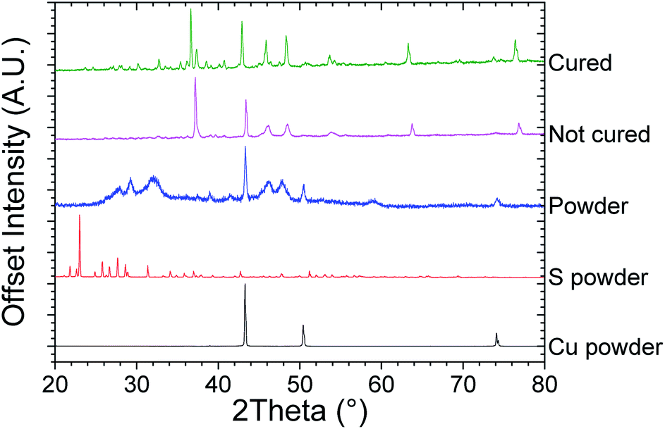 | ||
| Fig. 1 X-ray diffraction of purchased Cu and S powders, ball milled 1.97Cu + 1S (powder), printed ink using the ball milled powder in a water and sodium carboxymethylcellulose based ink (not cured) and the printed sample after being cured at 550 K in a He atmosphere (cured). | ||
XPS of all the samples are shown in Fig. S2,† whilst the printed Cu1.98S is represented in Fig. 2. The sulfur region is shown in Fig. 2a where the S(2p) envelope shows a strong doublet with the S(2p3/2) centered at 161.6 eV, which is typical of Cu2S species.32 Ground chalcocite has been previously shown to offer a complex surface chemistry, which is again observed in this case.33 S(2p3/2) doublets present at 162.7, 164.9 and 168.2 eV are assigned to metal deficient sulfides, polysulfides and sulfate/thiosulfate respectively.33,34 The copper region is shown in Fig. 2c where the Cu 2p envelope is in all cases dominated by the Cu(2p3/2) peak at 932.5 eV. On its own, and with small satellites observed, this peak is ambiguous as Cu(I) or Cu(0). The principal Auger line shown in Fig. 2e, however, is consistently noted at a kinetic energy of 917.4 eV, which is consistent with a Cu(I) species.35 The spectra show, however, that these samples exhibit a significant Cu(II) signal indicating the presence of a significant portion of CuO and/or CuS. This reveals that printing the inks at 413 K was insufficient to facilitate the complete formation of Cu2−xS.
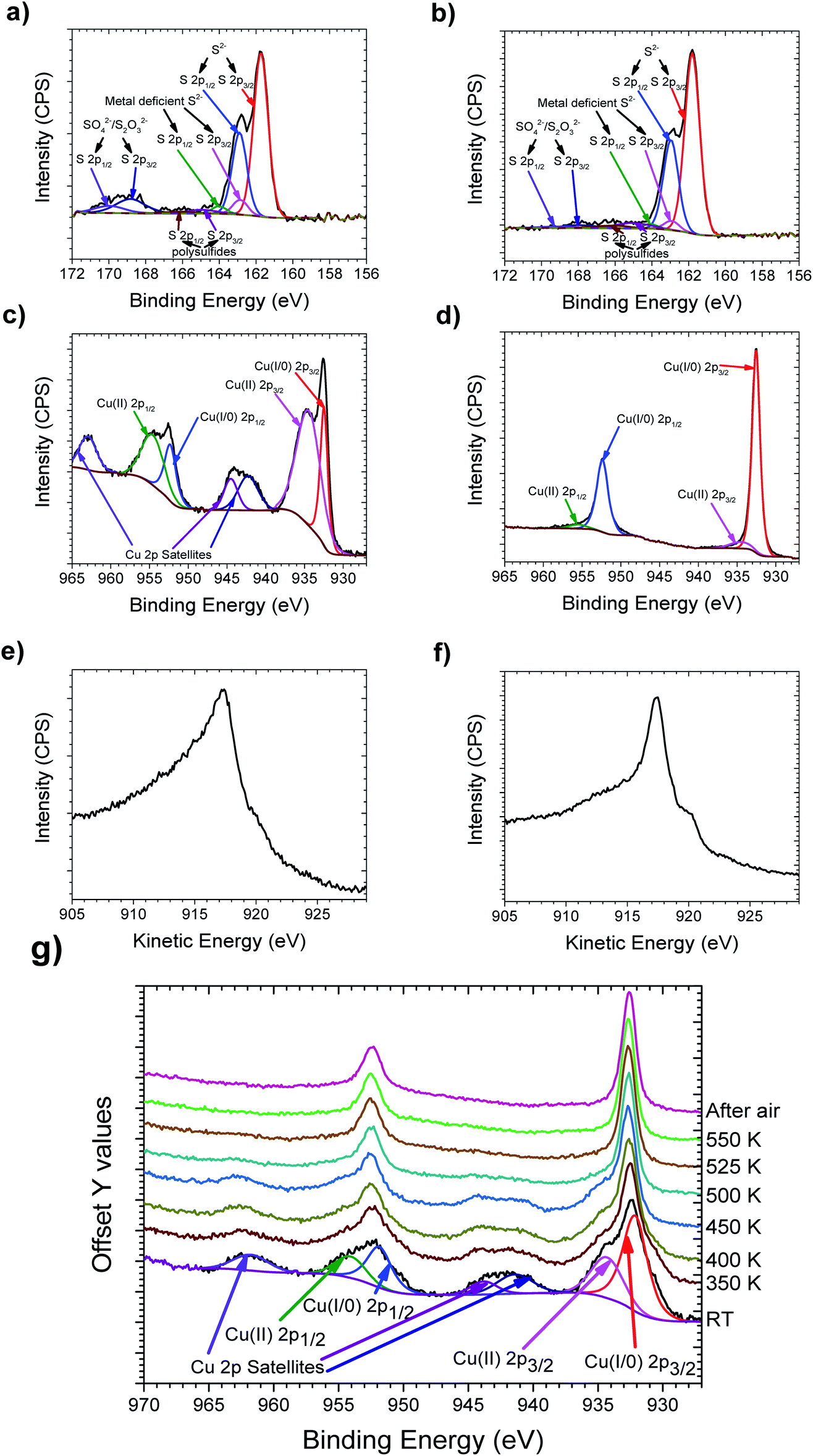 | ||
| Fig. 2 XPS analysis of printed Cu1.98S, where a, c, e and g have been printed on a hot plate in air at 413 K and b, d and f have had a further curing step at 550 K in a He atmosphere. (a) and (b) fitted S 2p, (c) and (d) fitted Cu 2p, (e) and (f) Cu Auger, (g) XPS data of the Cu 2p region of a sample at increasing temperatures in a vacuum. | ||
The printed samples were then heated to 550 K in a He atmosphere at a heating rate of 0.5 K per minute and then were left to cool naturally. Once cool the samples were left in air for 2 weeks. XRD can be seen after this curing step in Fig. 1, which reveals that the peaks are sharper compared to the non-cured printed samples, whilst more peaks are also observed. The sharper peaks are indicative of an increased grain size, as shown by the Scherrer equation.36 The extra peaks are also a sign that the material is now significantly less amorphous. XPS of the cured samples, as shown in Fig. 2, shows that both the Cu(2p3/2) peak and principal Auger line sharpen, with a stronger Cu(I) contribution, whilst the Cu(II) peak observed at 934.6 eV, and its associated satellites are notably reduced. It is also notable that on curing, the sulfate component is reduced and the sulfide becomes more dominant. Therefore, it was concluded that whilst neither the ball milling process nor the printing process at 413 K in air is enough to make significantly pure Cu2−xS by themselves, when an addition of a brief curing step at 550 K in He is added, significantly pure Cu2−xS is made. The samples were also deemed to be stable in air at room temperature, due to the lack of observed oxidation after 2 weeks of air exposure.
To investigate the required curing temperature to facilitate the complete formation of Cu2−xS, a printed sample was placed on a heating stage in the vacuum chamber of the XPS. This was then heated from 350 K to 550 K in 50 K increments to investigate the changes in the oxidation state of the sample. The Cu 2p energy region can be seen in Fig. 2g, whilst the Cu Auger and the S binding region can be seen in Fig. S3.† A gradual removal of the Cu(II) 2p peaks can be seen up to 500 K where these peaks are seen to be notably removed. An extra spectrum at 525 K and the spectrum at 550 K are then both consistent with the spectrum observed at 500 K. This therefore indicates a curing temperature of 500 K is sufficient to facilitate the formation of significantly pure Cu2−xS. It is of note that this change was permanent, as the XPS spectrum was consistent when measured at room temperature after the sample had been exposed to the atmosphere.
Compositional analysis of printed samples
The compositional analysis of the initial printed Cu2−xS samples from XPS can be seen in Fig. 3a, which indicates a large Cu excess when compared to the desired composition of Cu2S or Cu2S with a slight Cu deficiency. In contrast, elemental composition derived from EDX for these samples, as seen in Fig. 3b, can be seen to be of the intended stoichiometry within the margin of error for EDX. The contradictory results of the two techniques can be explained as XPS is a surface sensitive technique, with a penetration depth of 10 nm. EDX in contrast, has a penetration depth of over a micron which gives stoichiometry more representative of the bulk. This post printing Cu enrichment of the surface is thought to occur due to preferential loss of lighter S over Cu in water evaporation from the surface during the drying process. After curing at 550 K in a He atmosphere this Cu surface enrichment is seen to disappear as XPS reveals a composition near stoichiometry, which is consistent with the EDX measurement of the bulk at this stage.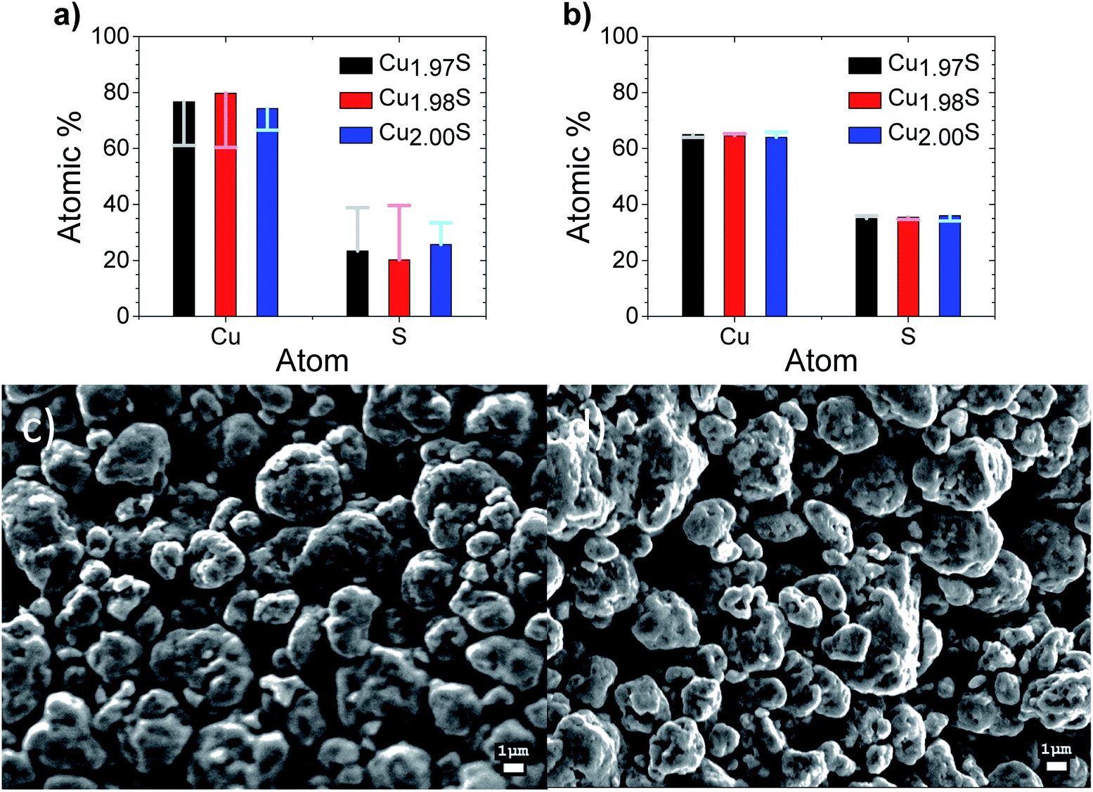 | ||
| Fig. 3 Compositional analysis of printed Cu2−xS samples (a) XPS composition of samples before (columns) and after curing (bars), and (b) EDX composition of samples before (columns) and after curing (bars). SEM of printed Cu2−xS samples (c) Cu1.97S not cured, (d) Cu1.97S cured. | ||
Scanning electron microscopy (SEM) images of the printed Cu1.97S samples both before and after curing at 550 K in He are shown in Fig. 3c and d respectively, with all the samples shown in Fig. S4.† The films are seen to be porous with what appears to be randomly orientated particles. This morphology appears to be unaltered through the various compositions and between the curing states.
Thermoelectric characterisation
Thermoelectric characterization of the printed Cu2−xS samples can be seen in Fig. 4. Electrical conductivity is shown in Fig. 4a and reveals that higher levels of S deficiency led to higher electrical conductivity. This can be rationalised as the removal of S from Cu2S leads to the introduction of extra holes into the material,9 which provides a lower resistance conduction pathway. Interestingly, three distinct condition regimes can be observed in the Cu2−xS samples, which correlate with the 3 known phases of Cu2−xS in the temperature regions studied.10 The first is from room temperature to 370 K, where the electrical conductivity increases with increasing temperature. This conduction below 370 K is typical of an intrinsic semiconductor and can be attributed to the low chalcocite γ phase (L-chalcocite). From 370 K to 700 K the Cu2−xS materials in general exhibit a drop in electrical conductivity with increase in temperature, which is consistent with the metallic behaviour of the high chalcocite β phase (H-chalcocite) through this temperature range.9 An outlier in this trend can be seen in the electrical data at around 600 K, however, this is likely due to a sintering effect enlarging the grain size. This would thus lower the contact resistance at the grains. This occurs at 600 K, higher than the 550 K manufacturing temperature of the thermoelectric elements. A major thermal degradation of sodium carboxymethylcellulose also occurs between 523 K and 648 K,37 so this outlier could also be caused by the removal of any remaining insulating binder. This observation indicates that a curing temperature in excess of 550 K may yield an improvement in measured power factors. Finally, above 700 K, Cu2S changes phase to an α phase with a face centered cubic structure, which exhibits largely temperature independent electrical conductivity. As would be expected, the trend in Seebeck coefficient versus Cu deficiency is the inverse to the trend seen in electrical conductivity. This is due to the Seebeck coefficient and electrical conductivity having an inverse and direct correlation to carrier concentration respectively.38 The resultant power factor is seen to be highest in Cu1.97S, especially in the α phase. Thermal conductivity is seen to be similar across all stoichiometry levels, with Cu2S exhibiting the lowest thermal conductivity values. This slightly lower thermal conductivity would be expected due to lower number of charge carries resulting in a lower electronic thermal conductivity,38 an observation that is also seen in spark plasma sintered samples.9 This results in the ZT reflecting a similar trend to the power factor.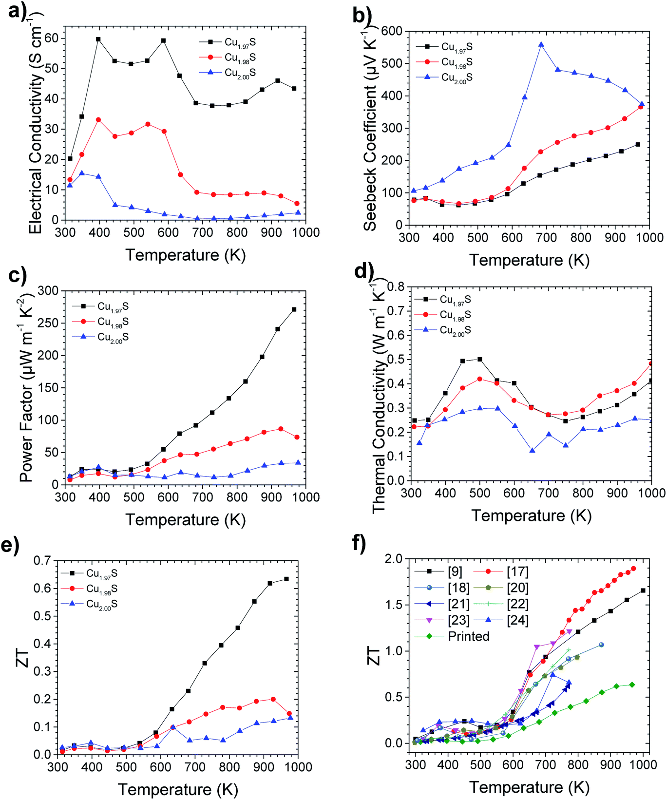 | ||
| Fig. 4 Thermoelectric performance of pseudo-3D printed Cu2−xS with varying stoichiometries: (a) electrical conductivity, (b) Seebeck coefficient, (c) power factor, (d) thermal conductivity (κ), (e) figure of merit, (f) figures of merit of printed Cu1.97S versus literature Cu2−xS values, where multiple values were reported, the highest value was used for comparison. | ||
After measurement of the thermoelectric properties at 1000 K, segregation of metallic copper could be visually observed in the samples. This is consistent with observations seen previously in the literature and highlights the instability of Cu2−xS at high temperatures.39,40 A cycling of the thermoelectric properties consequently saw a drop in thermoelectric performance, as highlighted in Fig. S6.†
When comparing the ZT results of printed Cu1.97S to literature values of Cu2−xS, as shown in Fig. 4f, printed Cu2−xS exhibits lower ZT values compared to other more time, energy and cost intensive manufacturing techniques. Na+ doping of Cu2−xS from sodium carboxymethylcellulose, could potentially in part explain the lower ZT values observed. The most significant cause of the diminished ZT values is, however, likely due to the low density of the samples. This resulted in lower electrical conductivity, compared to spark plasma sintered samples.9 The density of the printed samples were measured to be 4.5 g cm−3 (Fig. S5b†), making them 80% dense.41 This resulted in the high level of porosity which can be observed in the SEM images (Fig. 3).
Printed Cu1.97S still exhibits a peak ZT of 0.63 ± 0.09 at 966 K however, which is one of the highest numbers ever reported for a printed sample and the highest for a printed non-toxic or earth abundant material.42 In addition, this is the first example of a bulk printed thermoelectric material (as required for efficient thermoelectric generators), that is either non-toxic or Earth abundant, of which Cu2−xS is both.
Conclusions
In conclusion, bulk Cu2−xS samples were printed from ball milled constituent elements. The printed samples presented multiple Cu oxidation states, indicating the lack of purity of Cu2−xS initially. Following a cure at 550 K in He these additional oxidation states were seen to significantly diminish, leaving relatively pure Cu2−xS samples. SEM of the printed samples showed that the samples exhibit a porous nature, whilst XPS and EDX revealed that the composition of the samples had the same stoichiometry as the precursor powder formulation. The thermoelectric properties of the printed samples were investigated and revealed a peak ZT of 0.63 ± 0.09 at 966 K for Cu1.97S, which is the highest ZT recorded for a printed earth abundant material, whilst also being the highest ZT ever reported for a printed non-toxic material.Conflicts of interest
There are no conflicts to declare.Acknowledgements
The authors wish to thank EPSRC (EP/N020863/1) for funding. NPL and SM wish to thank the Welsh Government, ERDF and SMARTExpertise Wales for funding MACH1 and COMET. MJC would like to thank ERDF and WEFO for funding of SPARC II. All authors acknowledge the SU AIM Facility (EPSRC EP/M028267/1) for microscopy and imaging facilities. The authors would like to thank COATED2 (EPSRC EP/L015099/1) for purchasing the ULVAC ZEM-3.Notes and references
- J. Besseling and H. Pershad, The potential for recovering and using surplus heat from industry Final Report, London, 2014 Search PubMed.
- DEFRA, Act on CO2 Calculator: Public Trial Version Data, Methodology and Assumptions Paper, 2007 Search PubMed.
- D. Miorandi, S. Sicari, F. De Pellegrini and I. Chlamtac, Ad Hoc Netw., 2012, 10, 1497–1516 CrossRef.
- V. Leonov and R. J. M. Vullers, J. Electron. Mater., 2009, 38, 1491–1498 CrossRef CAS.
- D. A. Wright, Nature, 1958, 181, 834 CrossRef.
- A. F. Joffe and L. S. Stil’bans, Rep. Prog. Phys., 1959, 22, 306 CrossRef.
- CRC Handbook of Chemistry and Physics, ed. D. R. Lide, CRC Press, Boca Raton, FL, USA, 85th edn, 2005 Search PubMed.
- U. Tinggi, Toxicol. Lett., 2003, 137, 103–110 CrossRef CAS PubMed.
- Y. He, T. Day, T. Zhang, H. Liu, X. Shi, L. Chen and G. J. Snyder, Adv. Mater., 2014, 26, 3974–3978 CrossRef CAS PubMed.
- Q. Xu, B. Huang, Y. Zhao, Y. Yan, R. Noufi and S.-H. Wei, Appl. Phys. Lett., 2012, 100, 061906 CrossRef.
- S. Kashida, W. Shimosaka, M. Mori and D. Yoshimura, J. Phys. Chem. Solids, 2003, 64, 2357–2363 CrossRef CAS.
- H.-T. Zhang, G. Wu and X.-H. Chen, Langmuir, 2005, 21, 4281–4282 CrossRef CAS PubMed.
- M. Peng, L.-L. Ma, Y.-G. Zhang, M. Tan, J.-B. Wang and Y. Yu, Mater. Res. Bull., 2009, 44, 1834–1841 CrossRef CAS.
- Z. Li, W. Chen, H. Wang, Q. Ding, H. Hou, J. Zhang, L. Mi and Z. Zheng, Mater. Lett., 2011, 65, 1785–1787 CrossRef CAS.
- H. Lee, S. W. Yoon, E. J. Kim and J. Park, Nano Lett., 2007, 7, 778–784 CrossRef CAS PubMed.
- M. Salavati-Niasari, S. Alizadeh, M. Mousavi-Kamazani, N. Mir, O. Rezaei and E. Ahmadi, J. Cluster Sci., 2013, 24, 1181–1191 CrossRef CAS.
- L. Zhao, X. Wang, F. Y. Fei, J. Wang, Z. Cheng, S. Dou, J. Wang and G. J. Snyder, J. Mater. Chem. A, 2015, 3, 9432–9437 RSC.
- D. Yang, X. Su, Y. Yan, J. He, C. Uher and X. Tang, APL Mater., 2016, 4, 116110 CrossRef.
- R. Mulla and M. K. Rabinal, Ultrason. Sonochem., 2017, 39, 528–533 CrossRef CAS PubMed.
- S. Wu, J. Jiang, Y. Liang, P. Yang, Y. Niu, Y. Chen, J. Xia and C. Wang, J. Electron. Mater., 2017, 46, 2432–2437 CrossRef CAS.
- Y.-Q. Tang, Z.-H. Ge, J. Feng, Y.-Q. Tang, Z.-H. Ge and J. Feng, Crystals, 2017, 7, 141 CrossRef.
- Y.-Q. Tang, K. Zhang, Z.-H. Ge and J. Feng, J. Solid State Chem., 2018, 265, 140–147 CrossRef CAS.
- L.-J. Zheng, B.-P. Zhang, H. Li, J. Pei and J.-B. Yu, J. Alloys Compd., 2017, 722, 17–24 CrossRef CAS.
- Y. Yao, B.-P. Zhang, J. Pei, Y.-C. Liu and J.-F. Li, J. Mater. Chem. C, 2017, 5, 7845–7852 RSC.
- C. Han, G. Tan, T. Varghese, M. G. Kanatzidis and Y. Zhang, ACS Energy Lett., 2018, 3, 818–822 CrossRef CAS.
- Z. Cao, E. Koukharenko, M. J. Tudor, R. N. Torah and S. P. Beeby, Sens. Actuators, A, 2016, 238, 196–206 CrossRef CAS.
- F. Jiao, C. Di, Y. Sun, P. Sheng, W. Xu and D. Zhu, Philos. Trans. R. Soc., A, 2014, 372, 20130008 CrossRef PubMed.
- F. Kim, B. Kwon, Y. Eom, J. E. Lee, S. Park, S. Jo, S. H. Park, B.-S. Kim, H. J. Im, M. H. Lee, T. S. Min, K. T. Kim, H. G. Chae, W. P. King and J. S. Son, Nat. Energy, 2018, 3, 301–309 CrossRef CAS.
- M. R. Burton, S. Mehraban, D. Beynon, J. McGettrick, T. Watson, N. P. Lavery and M. J. Carnie, Adv. Energy Mater., 2019, 1900201 CrossRef.
- M. R. Burton, T. Liu, J. McGettrick, S. Mehraban, J. Baker, A. Pockett, T. Watson, O. Fenwick and M. J. Carnie, Adv. Mater., 2018, 30, 1801357 CrossRef PubMed.
- A. Smakula and V. Sils, Phys. Rev., 1955, 99, 1744–1746 CrossRef CAS.
- A. V. Naumkin, A. Kraut-Vass, S. W. Gaarenstroom and C. J. Powell, NIST X-ray Photoelectron Spectroscopy Database, https://srdata.nist.gov/xps/, accessed 4 June 2019 Search PubMed.
- S. Zhao and Y. Peng, Powder Technol., 2012, 230, 112–117 CrossRef CAS.
- I. Nakai, Y. Sugitani, K. Nagashima and Y. Niwa, J. Inorg. Nucl. Chem., 1978, 40, 789–791 CrossRef CAS.
- S. W. Goh, A. N. Buckley, R. N. Lamb, R. A. Rosenberg and D. Moran, Geochim. Cosmochim. Acta, 2006, 70, 2210–2228 CrossRef CAS.
- A. L. Patterson, Phys. Rev., 1939, 56, 978–982 CrossRef CAS.
- N. Ahmad, R. Wahab and S. Y. Al-Omar, Eur. J. Chem., 2014, 5, 247–251 CrossRef.
- G. J. Snyder and E. S. Toberer, Nat. Mater., 2008, 7, 105–114 CrossRef CAS PubMed.
- G. Dennler, R. Chmielowski, S. Jacob, F. Capet, P. Roussel, S. Zastrow, K. Nielsch, I. Opahle and G. K. H. Madsen, Adv. Energy Mater., 2014, 4, 1301581 CrossRef.
- A. V. Powell, J. Appl. Phys., 2019, 126, 100901 CrossRef.
- P. Patnaik, Handbook of inorganic chemicals, McGraw-Hill, Burlington, New Jersey, 2003 Search PubMed.
- M. Orrill and S. LeBlanc, J. Appl. Polym. Sci., 2017, 134, 44256 CrossRef.
Footnote |
| † Electronic supplementary information (ESI) available: Supporting Information includes all XRD, XPS and SEM data, in addition, thermal diffusivity, density and ZEM-3 cycling data is also presented. All data created during this research are openly available from the Swansea University data archive at DOI: 10.5281/zenodo.3375554. See DOI: 10.1039/c9ta10064d |
| This journal is © The Royal Society of Chemistry 2019 |