Monocrystalline perovskite wafers/thin films for photovoltaic and transistor applications

Abstract
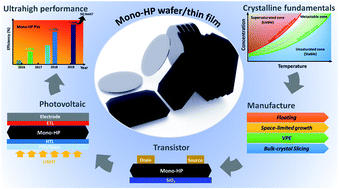
High-purity monocrystalline silicon has a long history in the development of photovoltaics; so far, it has dominant applications in modern computers with its profound implementations in transistors and chips. The success of silicon has shown that monocrystalline wafers/thin films of semiconducting materials with superior electronic properties are a good platform for optoelectronic and electronic applications. Recently, the newly emerging semiconducting materials of halide perovskites (HPs) have attracted considerable attention owing to their continuing success in high-efficiency solar cells. The demonstrated optoelectronic properties of HPs indicate that it could be a promising alternative to the silicon-based semiconducting industry. However, the prerequisite of high-efficiency devices is the material accessibility of monocrystalline HPs (mono-HPs), as per the lessons learned from monocrystalline silicon. Current HPs-based technologies, in terms of research areas such as solar cells, photodetectors, light-emitting diodes (LEDs), lasers, and transistors, suffer a bottleneck in manufacturing mono-HP wafers/thin-film materials; hence, exciting results involving mono-HP devices are absent. State-of-the-art optoelectronic HP-based devices are exclusively built using polycrystalline thin films, which are limited in their performance due to issues such as grain-boundary defects, large trap density, and inhomogeneous charge transport. However, these issues can be resolved by utilizing mono-HPs. In this review, we provide in-depth analyses and discussions on the potential of mono-HPs in photovoltaics and transistor applications, and we present the remaining challenges, as well as promising research strategies, to provide a direction for future programs.
- This article is part of the themed collection: Recent Review Articles
 Please wait while we load your content...

