
 Open Access Article
 This Open Access Article is licensed under a
 Creative Commons Attribution 3.0 Unported Licence
Enhanced performance of ZnO nanoparticle decorated all-inorganic CsPbBr3 quantum dot photodetectors†
Kai
Shen
 a,
Xiao
Li
a,
Hao
Xu
*a,
Mingqing
Wang
b,
Xiao
Dai
c,
Jian
Guo
d,
Ting
Zhang
e,
Shibin
Li
e,
Guifu
Zou
c,
Kwang-Leong
Choy
*b,
Ivan P.
Parkin
d,
Zhengxiao
Guo
dfg,
Huiyun
Liu
a and
Jiang
Wu
*ah
a,
Xiao
Li
a,
Hao
Xu
*a,
Mingqing
Wang
b,
Xiao
Dai
c,
Jian
Guo
d,
Ting
Zhang
e,
Shibin
Li
e,
Guifu
Zou
c,
Kwang-Leong
Choy
*b,
Ivan P.
Parkin
d,
Zhengxiao
Guo
dfg,
Huiyun
Liu
a and
Jiang
Wu
*ah
aDepartment of Electronic and Electrical Engineering, University College London, Torrington Place, London WC1E 7JE, UK. E-mail: hao.xu.15@ucl.ac.uk; jiangwu@uestc.edu.cn
bInstitute for Materials Discovery, University College London, Torrington Place, London WC1E 7JE, UK. E-mail: k.choy@ucl.ac.uk
cSchool of Energy, Soochow Institute for Energy and Materials Innovations, Key Laboratory of Advanced Carbon Materials and Wearable Energy Technologies of Jiangsu Province, Soochow University, Suzhou 215006, China
dDepartment of Chemistry, University College London, 20 Gordon Street, Bloomsbury, London WC1H 0AJ, UK
eState Key Laboratory of Electronic Thin Films and Integrated Devices, School of Optoelectronic Information, University of Electronic Science and Technology of China (UESTC), Chengdu, Sichuan 610054, China
fDepartments of Chemistry and Mechanical Engineering, The University of Hong Kong, Hong Kong SAR, China
gZhejiang Institute of Research and Innovation, The University of Hong Kong, Qingshan Lake SciTech City, Hangzhou, China
hInstitute of Fundamental and Frontier Science, University of Electronic Science and Technology of China, Chengdu 610054, P. R. China
First published on 25th February 2019
Abstract
All-inorganic perovskite quantum dots have attracted substantial attention due to their excellent optical properties. However, the surface states of colloidal quantum dots and the insufficient carrier transport in a quantum dot film hinder their further development. Here, solution-processed CsPbBr3/ZnO quantum dot/nanoparticle nanocomposites are used to lessen the impact of surface states as well as facilitate charge transport. The blending of ZnO nanoparticles during CsPbBr3 quantum dot synthesis results in improved optical properties as well as film formation that enhances charge transport. A photodetector based on the CsPbBr3/ZnO/glassy-graphene heterostructure is fabricated, which exhibits an enhanced photoresponse and distinct self-powered operation with an open-circuit voltage as large as 150 mV. Most importantly, an excellent stability of the hybrid nanoparticle/quantum dot photodetector is reported and consistent high performance with marginal degradation is achieved for more than 7 months.
Introduction
Photodetectors play an important role in a wide range of applications, such as optical communication, environmental monitoring, imaging and biochemical sensing.1–4 Various semiconductors have been employed in photodetectors, such as GaN, Si and InGaAs.5–7 Although the technologies of commercial photodetectors are mature and reliable, there has been increasing interest in developing cost-effective photodetectors using emerging materials as alternatives to conventional ones in the state-of-the-art photodetectors.Recently, organolead halide perovskites (OHPs), a family of cost-effective and high-throughput materials, have been extensively explored for optoelectronic devices, including solar cells, light emitting diodes (LEDs), and photodetectors, owing to their excellent optoelectronic properties, such as tunable direct band gaps, large absorption coefficients, high carrier mobility, and long diffusion lengths.8–11 Within a few years, halide perovskite based photovoltaic devices have achieved impressive power conversion efficiencies as high as 23.6%.12 However, OHPs are unstable in ambient air and sensitive to moisture and heat, causing significant degradation and hindering their further development. In comparison, all-inorganic halide perovskite, cesium lead halide (CsPbX3, X = Cl, Br, I), quantum dots (QDs) not only inherit the advantages of OHPs, but also exhibit better thermal stability.9,13 For example, Liu et al. presented photodetectors made of CsPbCl3 nanocrystals, which exhibited a good photoresponse to UV light.14 Han and co-workers reported CsPbBr3 microcrystal based photodetectors with high on/off ratios as well as a fast response speed,15 and Fan et al. demonstrated CsPbI3 nanowire configured array-photodetectors, which had a stabilized cubic phase and exhibited high responsivity.16 Apart from that, the excellent emission efficiency and tunable emission color of CsPbX3 QDs benefit from the quantum size effect and anion exchange, and make them potential candidates in high quantum efficiency and low-cost LEDs.13,17,18 Particularly, CsPbBr3 exhibits better environmental stability, which does not need to be synthesized in a glove box with a N2 atmosphere to prevent degradation.18–21 However, CsPbBr3 QDs, the same as general colloidal QDs, are prone to a high density of trap states which are detrimental to device performance.22,23 On the other hand, the insulating barriers, produced by a large number of long ligand chains or dangling bonds in CsPbBr3 QDs, significantly mitigate efficient carrier transport. Therefore, new ligand or passivation strategies are highly desirable and being sought to promote the carrier transport as well as lower surface state densities and associated surface recombination. To date, atomic-ligand and hybrid passivation schemes have been demonstrated by introducing monovalent halide anions and organic crosslinks, but they are time-consuming and the synthesis was at relatively high temperature, not suitable for flexible devices.24,25
In this work, cost-effective and solution-processed CsPbBr3 QDs were synthesized immediately followed by in situ blending of ZnO nanoparticles (NPs) at room temperature without the use of an inert gas. The ZnO NP blended CsPbBr3 QD film clearly exhibits improvement in crystal quality, in terms of grain boundaries. The blending of ZnO NPs also reduces surface trap states and enables increased control over the balance of charges on the surface of the QDs, which leads to an increase in carrier transport. Photodetectors based on the hybrid CsPbBr3 QDs/ZnO NPs show enhanced performance, including higher photocurrent, lower dark current, better photoresponsivity and faster response speeds. Most importantly, the photodetectors exhibit excellent stability after being stored in air for more than 7 months, which is promising for practical perovskite-based devices and further promotes their potential commercialization.
Results and discussion
The hybrid of CsPbBr3 QDs/ZnO NPs was synthesized by an optimized one-step injection method at room temperature.26 A Cs+ precursor was prepared by dissolving Cs2CO3 powder in propionic acid (PrAc), and PbBr2 powder was dissolved into a mixture of solvents of butylamine (BuAm), isopropanol (IPrOH) and PrAc to prepare a PbBr2 precursor, as illustrated in the schematic flowchart in Fig. 1a. The PbBr2 precursor was then mixed with the Cs+ precursor, hexane (HEX) and PrAc, which immediately turned yellow after stirring and was centrifuged and dispersed in toluene 3 times to remove irrelevant solvents. ZnO NPs dispersed in chloroform were injected into CsPbBr3 QD solution. Subsequently, ZnO NP blended CsPbBr3 QD films were prepared using spin coating followed by annealing. Transmission electron microscopy (TEM) was employed to investigate the crystal quality of the as-prepared perovskite QDs. A representative TEM image of CsPbBr3 QDs is shown in Fig. 1b, in which well-crystallized dots without any lattice distortion or crystal defects were observed. The average size of the as-prepared nanocomposites is measured to be ∼9 nm (Fig. S1, ESI†). Furthermore, chemical compositions (Cs, Pb, Br, Zn and O) and their distributions were analyzed by energy dispersive X-ray spectroscopy (EDX) in a zoomed-out area as shown in Fig. 1c. Each element, particularly Zn and O, is uniformly and well distributed in the observed area, confirming that ZnO NPs and CsPbBr3 QDs were uniformly mixed. | ||
| Fig. 1 Synthesis, and structural and film properties of the CsPbBr3 QDs blended with ZnO NPs. (a) Schematic representation of the growth process of the CsPbBr3 QDs. (b) High resolution TEM image of the CsPbBr3 QDs. The scale bar is 10 nm. (c) A low magnification TEM image of the CsPbBr3 QDs and element mapping within this area by EDX. The scale bar in the low magnification TEM image is 200 nm. (d) SEM images of CsPbBr3 QD films with different amounts of ZnO NPs: pure CsPbBr3 QDs, and CsPbBr3 QDs with 20 μL ZnO, 40 μL ZnO, 60 μL ZnO, 80 μL ZnO and 100 μL ZnO. The scale bar is 1 μm. | ||
Fig. 1d shows the surface morphology evolution of CsPbBr3 QD films after introducing ZnO NPs, obtained from scanning electron microscopy (SEM). As shown in Fig. 1d, the film surface of pristine QDs without ZnO NPs is comprised of large grains with an average dimension of circa 1 μm, which resulted from clustering or agglomeration of CsPbBr3 QDs. Long grain boundaries and large pinholes were observed as well, indicative of the relatively poor coverage of the film on the substrate. In contrast, via blending more ZnO NPs by increasing the injection volume from 20 μL to 100 μL but at the same concentration, the perovskite films possessed smaller grains and fewer pinholes. Additionally, the increase in ZnO NP blending gradually results in a more compact film and thus better surface coverage, as depicted in Fig. 1d and S2.† This significant improvement of surface morphology reveals successful binding of CsPbBr3 QDs by ZnO NPs, which is potentially advantageous to reduce grain boundaries and facilitate charge transfer as a result of the high conductivity of ZnO NPs.
The as-prepared materials were studied by powder X-ray diffraction (PXRD). In Fig. 2a, CsPbBr3 QD films exhibit almost unchanged XRD peaks before and after injecting ZnO NPs. The characteristic peaks at 15.1°, 21.45° and 30.7° were assigned to the (110), (112) and (220) planes of the crystalline orthorhombic CsPbBr3 perovskite (ICSD # 97851), respectively, consistent with reported work.26 The dominant peaks with a full-width at half-maximum (FWHM) of ∼0.5° not only indicate the uniformity of QDs but also the high crystallinity of the CsPbBr3 QD films. Notably, there is an additional peak located at 11.65°, which could be attributed to the formation of CsPb2Br5 or excess PbBr2.27,28 By adding ZnO NPs, this peak tends to be reduced due to the capping of CsPbBr3 QDs with ZnO NPs, which protects CsPbBr3 QDs from reacting with excess Pb2+ and Br− ions.29
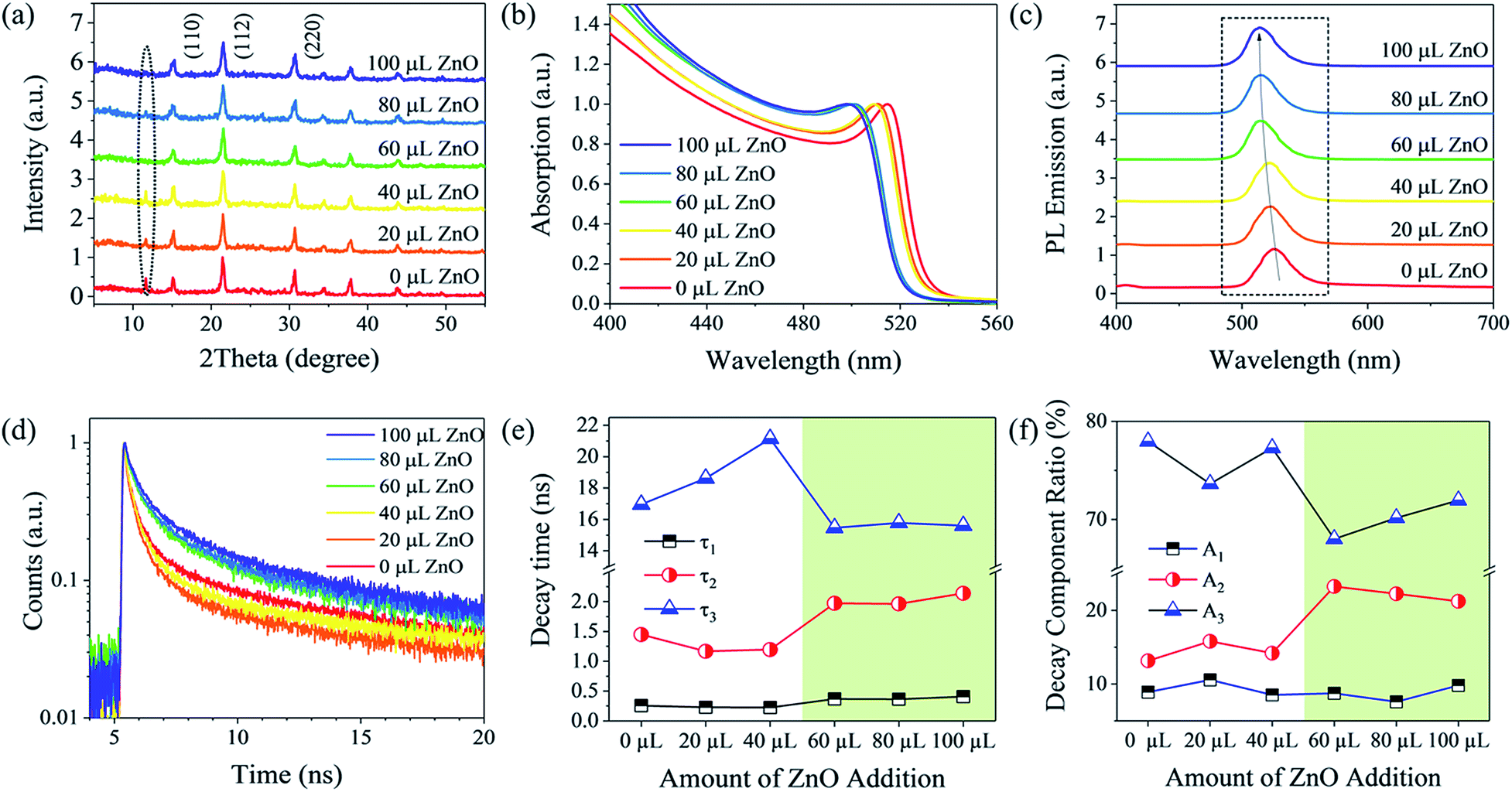 | ||
| Fig. 2 Structural and optical characterization of ZnO NP blended CsPbBr3 QDs. (a) XRD patterns. (b) Absorption spectra. (c) Steady-state PL spectra. (d) Time-resolved PL measurement. Each color represents the different quantities of ZnO NPs involved. The excitation laser wavelength is 405 nm. (e) Decay times and (f) decay component ratios extracted from the TRPL spectra in (d) as a function of the amount of ZnO NPs added to the CsPbBr3 QDs. | ||
In order to gain further insight into the optical properties of CsPbBr3 QD films with ZnO NPs, UV-Vis spectroscopy, photoluminescence (PL) and time-resolved PL (TRPL) measurements were performed. In Fig. 2b, the steady-state absorption spectrum of pure CsPbBr3 QDs exhibits a sharp absorption edge at 531 nm, corresponding to a direct bandgap of 2.34 eV, slightly higher than that of their bulk counterparts due to the quantum size effect.9,30 After introducing 20 μL to 100 μL of ZnO NPs, the absorption edges gradually shifted to shorter wavelengths. This blue shift indicates the formation of CsPbBr3 QDs/ZnO NP nanocomposites and hence stronger quantum confinement of charges, i.e., holes, in CsPbBr3 QDs/ZnO NPs. PL spectra excited using a 405 nm laser are illustrated in Fig. 2c, in which an evident peak at 526.9 nm with a narrow FWHM of 29.1 nm was identified for the pure CsPbBr3 QDs. It was observed that the PL emission peak of the ZnO NP blended CsPbBr3 QD film shifts from 526.9 nm to 514 nm after increased injection of ZnO NPs, in good agreement with the absorption spectra (Fig. 2b). Moreover, the ZnO NP blended CsPbBr3 QD films possessed narrower FWHMs of PL spectra, indicating the better uniformity of QDs owing to suppressing agglomeration of CsPbBr3 QDs (Fig. S3, ESI†). In order to understand charge carrier dynamics and confirm the benefits of adding ZnO NPs, TRPL spectra of CsPbBr3 QDs were obtained (Fig. 2d), which can be fitted with a multi-exponential decay function with three decay components. These three time constants τ1, τ2 and τ3 obtained by the fitting are summarized in Table S1.† The average decay lifetimes of CsPbBr3 QDs with an increasing amount of ZnO NPs can be calculated as 13.431, 13.921, 16.530, 11.006, 11.536 and 11.724 ns, respectively. A shorter decay time, benefiting from the reduced carrier trapping by surface states, is important for fast photodetectors. To understand the carrier dynamics of CsPbBr3 QDs after blending ZnO NPs, the decay times and the ratios of each decay component are plotted in Fig. 2e and f. The fastest decay time, τ1, and the ratio of this decay component are barely changed. This decay time is most likely associated with non-radiative recombination, as the crystal quality of the CsPbBr3 QDs should not be influenced by ZnO NPs. The ratio of this decay is the lowest, which again indicates high crystal quality of the CsPbBr3 QDs. The time constants τ2 and τ3 have a distinct dependence on the amount of ZnO NPs incorporated into the QDs. The former, τ2, is about 1–2 ns, which can be assigned to typical radiative recombination.31 The long decay time, τ3, of over 10 ns may be caused by the surface trap states of CsPbBr3 QDs. From Fig. 2e and f, it can be seen that the increase of ZnO NPs (>40 μL) clearly leads to reduction of τ3 and reduced ratios of surface trap-related decay or increased ratios of radiative recombination, suggesting surface passivation of CsPbBr3 QD films by ZnO NPs. It should be noted that the increase in τ2 and relatively low ratio of radiative combination even after incorporating ZnO NPs is due to the type II CsPbBr3/ZnO band alignment and thus electrons transfer from CsPbBr3 QDs to ZnO NPs. In summary, the ZnO blended CsPbBr3 QDs, exhibit a better surface morphology, higher crystal quality, and lower trap states, and are promising for low-cost and solution-processed optoelectronics.
Photodetectors based on the CsPbBr3/ZnO QD/NP nanocomposites were fabricated on quartz substrates. The device structure is schematically shown in Fig. 3a. Glassy-graphene thin films, possessing excellent properties of transparency, conductivity, and chemical inertness, were employed as the electron transport layer and transparent electrode.32,33 Two devices, one based on perovskite QDs with 60 μL ZnO NPs (PGH_1) and the other based on perovskite QDs only (PGH_2), were studied. As shown in the inset of Fig. 3a, a device with glassy graphene electrodes shows good transparency. Fig. 3b shows the current–voltage (I–V) curves of PGH_1 measured in the dark, under white light, and under 405 nm and 520 nm laser illumination at room temperature, respectively. The linear dependence of I–V curves suggests good conductivity and efficient charge carrier transport between perovskite QDs and glassy-graphene. This is not the case when no ZnO NP was added, and a higher dark current and lower photocurrent were measured for device PGH_2 as shown in Fig. 3c. Notably, there is a distinct open circuit voltage when illuminated using lasers. At 405 nm illumination, the photovoltage of PGH_1 can be as high as 150 mV; however, the photovoltaic effect was not observed in the PGH_2 photodetector (Fig. S4, ESI†). This phenomenon can be assigned to the introduction of a built-in electric field by ZnO nanoparticles. As one of the key figures-of-merit, photoresponsivity, which can be expressed as RA = Iph/P (where Iph denotes the photocurrent and P represents the incident light intensity), was calculated and is plotted in Fig. 3d, as a function of applied voltage.33 The obtained largest photoresponsivity of the PGH_1 device at 1 V bias was 0.4 mA W−1 and 0.03 mA W−1 when illuminated using 405 nm and 520 nm lasers, respectively. The lower response at 520 nm is due to a lower absorption of photons with energy close to the band edge (Fig. 2b). The RA values of PGH_2 under different illuminations were both one order smaller than those of PGH_1 measured under the same conditions. The improved photocurrent and photoresponse again confirm the advantages of blending ZnO NPs in perovskite QDs.
 | ||
| Fig. 3 The overview and electrical performance of the CsPbBr3 and glassy-graphene heterostructure device. (a) Scheme of the architecture of the PGH photodetector (quartz/Au/Ni/Glassy-graphene/CsPbBr3/Ni/Au). The inset shows a device placed over the UCL Engineering logo, showing good transparency. (b) I–V characteristic curves of the PGH_1 device in the dark and under white light and different illuminations, 405 nm and 520 nm. (c) The photocurrent and dark current of the PGH_1 and PGH_2 photodetectors. (d) The calculated photoresponsivity of the two devices above under 405 nm and 520 nm illumination, respectively. | ||
The effects of introducing ZnO NPs on the detector performance were further investigated by atomic force microscopy (AFM) and conductive atomic force microscope (CAFM). The surface morphologies of the samples prepared with 0–80 μL ZnO NPs are displayed in Fig. 4a, respectively. Similar to the SEM images (Fig. 1d), it was observed that pinholes were gradually filled by ZnO NPs, so the surface of QD films became much more compact and smoother, consistent with the decreased surface roughness. Surface current maps were obtained by CAFM to evaluate ZnO NP treatment induced impacts on the electrical properties of films, as illustrated in Fig. 4b. Without adding ZnO NPs, higher current is measured for the QD films. On increasing the amount of ZnO NPs, the current gradually became lower and more uniform across the scanned area. This behavior can be explained by the illustration shown in Fig. 4c. Without ZnO NPs, clustering or agglomeration of CsPbBr3 QDs resulted in rough surfaces along with a high density of pinholes, which induced a high leakage current. These pinholes compromise lateral charge transfer and hence collection of photocurrent. The assumption can be well supported by the I–V characteristics shown in Fig. 3c. Blending ZnO NPs in the CsPbBr3 QDs prevented serious clustering or agglomeration of QDs and hence enabled the formation of compact and smooth films. Photocarriers generated in CsPbBr3 QDs can be more effectively transferred to the terminals when ZnO NPs bridge the gaps between the QDs. The ZnO NPs also function as a means of passivation. Consequently, the devices were able to have smaller leakage current and lower dark current but deliver higher photocurrent after ZnO NP treatment.
 | ||
| Fig. 4 Surface morphology characterization and passivation process of CsPbBr3. (a) Surface morphology of each sample with an increasing percentage of ZnO from 0 μL to 80 μL by AFM. (b) The corresponding current mapping. (c) Schematic process of applying ZnO NP passivation to the CsPbBr3 QD film. | ||
Typical I–V curves of PGH_1 photodetector under the 405 nm laser illumination with various power intensities are shown in Fig. 5a, exhibiting the apparent dependence on light intensity. With increasing light intensity, photocurrent was enhanced due to a larger population of photogenerated carriers. Power-dependent photocurrent is plotted in Fig. 5b, fitted by the power law (Iph ∝ Pβ, where β denotes the Duane plot slope). The best fitting gave a non-linear behavior of β = 0.502, which is associated with the increased recombination of photogenerated charge carriers at high light intensity. This indicates presence of some recombination centers within the perovskite.34,35 As shown in Fig. 2f, the non-radiative recombination time constant, τ1, barely changed after adding ZnO NPs, which requires further optimization of QD synthesis. Current–time (I–t) curves of transient photoresponse as a function of incident light intensity were measured and are plotted in Fig. 5c. It was observed that all the dynamic curves exhibited a sensitive and reproducible photoresponse, and the photocurrent continuously increased with the irradiation power raised from 1.3 mW cm−2 to 22.8 mW cm−2. Fig. 5d shows the photoresponsive dynamics of the PGH_1 photodetector at 1 V and −1 V bias illuminated using 405 nm and 520 nm lasers, respectively. A larger photocurrent was obtained at −1 V than 1 V bias, caused by the built-in electric field. Notably, the PGH_1 photodetector displayed an excellent photoresponse under 0 V bias (Fig. 5e), demonstrating self-powered operating mode enabled by the built-in electric field.
 | ||
| Fig. 5 Electrical properties of the PGH_1 photodetector. (a) I–V curves of the device illuminated using a 405 nm laser with the incident light intensity varied from 1.3 mW cm−2 to 22.8 mW cm−2. (b) The photocurrent measured as a function of incident light intensity and the corresponding power fitting curve. (c) The transient photocurrent response of the device illuminated using a 405 nm laser with varying power from 1.3 mW cm−2 to 22.8 mW cm−2 at 1 V bias. (d) The transient photoresponse curves of the PGH_1 photodetector under 405 nm and 520 nm illumination with an intensity of 22.8 mW cm−2. The applied voltages are 1 V and −1 V, respectively. (e) The transient photoresponse curves of the PGH_1 photodetector under 405 nm illumination at 0 V. (f) The corresponding rise and fall time under 1 V bias voltage. (g) The corresponding rise and fall time at 0 V bias. (h) The long-term stability of the PGH_1 photodetector over 7 months. (i) The transient photocurrent response of the device around the middle and end of the stability test. | ||
As displayed in Fig. 5f, the rise time (τrise) and fall time (τfall) of the PGH_1 device were determined to be less than 76.5 ms and 73.5 ms at 1 V bias, respectively, which reached the steady-state condition faster than the PGH_2 device (Fig. S5 and Table S3, ESI†). This pronounced enhancement was mainly attributed to faster charge separation and more efficient carrier transport at interfaces that resulted from surface passivation by ZnO NPs. As compared with previous reports, the photoresponse time of our ZnO NP blended PGH photodetectors is much shorter by two orders than that of all-inorganic perovskite based and 2-D material heterostructure based photodetectors,36–38 indicating the good light-switching behavior of the as-prepared devices. For self-powered photodetection (Fig. 5g), it was found that the fall time is almost unchanged while the rise time is obviously increased under 0 V bias (fitted by a single-exponential decay, Fig. S6 and Table S2, ESI†), which was probably due to the internal electric field not being strong enough to separate the electron–hole pair efficiently. The stability of perovskite-based devices is a critical factor for practical applications. To test the stability of the device reported in this study, the photocurrent of the PGH_1 photodetector was recorded over a seven-month period, as shown in Fig. 5h. The dark current maintained similar values between 1 nA and 5 nA, and the photocurrent still retained its initial value with negligible degradation after storing under ambient conditions for more than 7 months. Notably, the PGH_1 photodetector still displayed good reproducibility, as well as marginal degradation in response speed, after being stored under ambient conditions for over 7 months, as shown in Fig. 5i, exhibiting outstanding stability. In contrast, PGH_2 photodetectors significantly suffered from degradation, with respect to the response speed (Fig. S7 and Table S3, ESI†). This is mainly ascribed to the passivation of ZnO NPs. By comparing with other reported perovskite-based photodetectors,39–44 the ZnO NP decorated PGH photodetector achieves the best reported stability under ambient conditions.
Conclusions
In summary, CsPbBr3 QDs decorated by ZnO NPs were successfully synthesized by a simple non-vacuum solution-processed method. By introducing ZnO NPs, a better film surface morphology with fewer defects at the grain boundaries and fewer pinholes was achieved. Improved optical and electrical properties of CsPbBr3 QDs were observed after adding ZnO NPs. PGH photodetectors based on ZnO/CsPbBr3 hybrids were fabricated. The detectors exhibited excellent responsivity, fast photoresponsive on-off switching (<76.5 ms), and self-powered operating mode. Moreover, an outstanding stability over 7 months was achieved for our devices reported in this study, which could pave the way for future commercialization of perovskite-based optoelectronic applications.Experimental section
Chemicals
PbBr2 (99.9%), Cs2CO3 (99%), butylamine (BuAm, 99.5%), isopropanol (IPrOH, 99.5%), propionic acid (PrAc, 99.5%), N-hexane (HEX, 99.5%), toluene (99.8%) and ZnO nanoparticles (99.9%) were purchased from Sigma-Aldrich. Chloroform (99.9%) was purchased from Fisher Chemical. All chemicals were used as received without further purification.Material synthesis
Procedures involved in the preparation of ZnO NP blended CsPbBr3 QDs are carried out in ambient air at room temperature, as shown in Fig. 1a. A Cs+ precursor was prepared by dissolving Cs2CO3 powder (1.1736 g) in the PrAc (2 mL). Meanwhile, the PbBr2 powder (0.9175 g) was dissolved into a mixture of solvents of BuAm, IPrOH and PrAc (5 mL, 1![[thin space (1/6-em)]](https://www.rsc.org/images/entities/char_2009.gif) :1:1) to form the PbBr2 precursor. Subsequently, the PbBr2 precursor (270 μL) was swiftly injected into the solution mixture containing the Cs+ precursor (25 μL), IPrOH (5 mL) and HEX (10 mL). This solution turned light yellow within seconds. Subsequently, high-quality CsPbBr3 QDs were obtained by centrifuging and dispersing the as-prepared solution in toluene 3 times, in order to eliminate the trace of other solvents. Different centrifugation speeds of 1500 rpm, 2000 rpm and 1500 rpm for 2 min were used each time. Finally, different amounts of ZnO NP precursor (0.5 M, dissolved in chloroform) from the top of the clear solution were injected into the as-prepared CsPbBr3 QDs.
:1:1) to form the PbBr2 precursor. Subsequently, the PbBr2 precursor (270 μL) was swiftly injected into the solution mixture containing the Cs+ precursor (25 μL), IPrOH (5 mL) and HEX (10 mL). This solution turned light yellow within seconds. Subsequently, high-quality CsPbBr3 QDs were obtained by centrifuging and dispersing the as-prepared solution in toluene 3 times, in order to eliminate the trace of other solvents. Different centrifugation speeds of 1500 rpm, 2000 rpm and 1500 rpm for 2 min were used each time. Finally, different amounts of ZnO NP precursor (0.5 M, dissolved in chloroform) from the top of the clear solution were injected into the as-prepared CsPbBr3 QDs.
Materials characterization
Transmission electron microscopy (TEM) images and energy dispersive X-ray (EDX) mappings were obtained on a JEOL 2100 microscope attached with an X-MaxN detector (Oxford Instruments). The surface morphology of the samples was examined using an EVO LS15 scanning electron microscope (ZEISS). X-ray diffraction was recorded using a powder X-ray diffractometer (PXRD, Bruker D8 Discover) with CuKα1,2 radiation (λ = 1.54056 Å). Optical absorption spectra were measured using Lambda 750S UV-Vis spectrometers (Perkin Elmer) at room temperature. Steady-state and time-resolved PL spectra were obtained on a TCSPC (LifeSpec-ps) from Edinburgh Instruments with an excitation wavelength of 405 nm at −15 °C. The current mapping measurements were carried out on a Keysight 5600LS atomic force microscope (AFM) in the current sensing mode in the air.Device fabrication
Few-layer glassy-graphene (5 nm) was pre-deposited onto the quartz substrate by a polymer-assisted deposition (PAD) approach.32 The as-synthesized perovskite precursor was then spin-coated on the glassy-graphene coated substrate at 1000 rpm for 60 s. Subsequent deposition cycles were applied to increase the thickness of the absorbing layer. The samples were annealed at 120 °C for 1 min after each spinning, and baked at 120 °C for 5 min after spin coating of the last layer. The total thickness of the active layer was around 150 nm (8 deposition cycles). The heterojunction was formed at the interface where the perovskite and glassy-graphene were overlapped, with the dimension circa 2 mm by 5 mm. The Ni/Au (10/100 nm) electrodes were finally deposited through a shadow mask by thermal evaporation. The size of the metal contact pads was circa 1 mm by 4 mm.Device characterization
I–V characteristics of devices were determined using a Keithley 4200 semiconductor parameter analyzer and an attached probe station. Two laser diodes (405 nm and 520 nm) were employed as the illumination source, with the corresponding power intensity of 22.8 mW cm−2 and 10.5 mW cm−2, respectively. The spot size of the two laser diodes was estimated to be 0.75 mm in radius. During the measurements, all devices were kept at room temperature in the ambient atmosphere.Conflicts of interest
There are no conflicts to declare.Acknowledgements
The authors acknowledge the support of EPSRC grants (EP/L018330/1 and EP/P006973/1) and Innovate UK under Hi-prospect project (102470).References
- G. Konstantatos, I. Howard, A. Fischer, S. Hoogland, J. Clifford, E. Klem, L. Levina and E. H. Sargent, Nature, 2006, 442, 180–183 CrossRef CAS PubMed.
- G. Konstantatos and E. H. Sargent, Nat. Nanotechnol., 2010, 5, 391–400 CrossRef CAS PubMed.
- T. Rauch, M. Böberl, S. F. Tedde, J. Fürst, M. V. Kovalenko, G. Hesser, U. Lemmer, W. Heiss and O. Hayden, Nat. Photonics, 2009, 3, 332–336 CrossRef CAS.
- F. H. L. Koppens, T. Mueller, P. Avouris, A. C. Ferrari, M. S. Vitiello and M. Polini, Nat. Nanotechnol., 2014, 9, 780–793 CrossRef CAS PubMed.
- M. A. Khan, M. Shatalov, H. P. Maruska, H. M. Wang and E. Kuokstis, Jpn. J. Appl. Phys., 2005, 44, 7191–7206 CrossRef CAS.
- J. Michel, J. Liu and L. C. Kimerling, Nat. Photonics, 2010, 4, 527 CrossRef CAS.
- S. Maimon, E. Finkman, G. Bahir, S. E. Schacham, J. M. Garcia and P. M. Petroff, Appl. Phys. Lett., 1998, 73, 2003–2005 CrossRef CAS.
- M. M. Lee, J. Teuscher, T. Miyasaka, T. N. Murakami and H. J. Snaith, Science, 2012, 338, 643–647 CrossRef CAS PubMed.
- J. Song, J. Li, X. Li, L. Xu, Y. Dong and H. Zeng, Adv. Mater., 2015, 27, 7162–7167 CrossRef CAS PubMed.
- L. Dou, Y. M. Yang, J. You, Z. Hong, W. H. Chang, G. Li and Y. Yang, Nat. Commun., 2014, 5, 5404 CrossRef CAS PubMed.
- T. Zhang, J. Wu, P. Zhang, W. Ahmad, Y. Wang, M. Alqahtani, H. Chen, C. Gao, Z. D. Chen, Z. Wang and S. Li, Adv. Opt. Mater., 2018, 6, 1701341 CrossRef.
- K. A. Bush, A. F. Palmstrom, Z. J. Yu, M. Boccard, R. Cheacharoen, J. P. Mailoa, D. P. McMeekin, R. L. Z. Hoye, C. D. Bailie, T. Leijtens, I. M. Peters, M. C. Minichetti, N. Rolston, R. Prasanna, S. Sofia, D. Harwood, W. Ma, F. Moghadam, H. J. Snaith, T. Buonassisi, Z. C. Holman, S. F. Bent and M. D. McGehee, Nat. Energy, 2017, 2, 17009 CrossRef CAS.
- L. Protesescu, S. Yakunin, M. I. Bodnarchuk, F. Krieg, R. Caputo, C. H. Hendon, R. X. Yang, A. Walsh and M. V. Kovalenko, Nano Lett., 2015, 15, 3692–3696 CrossRef CAS PubMed.
- J. Zhang, Q. Wang, X. Zhang, J. Jiang, Z. Gao, Z. Jin and S. Liu, RSC Adv., 2017, 7, 36722–36727 RSC.
- B. Yang, F. Zhang, J. Chen, S. Yang, X. Xia, T. Pullerits, W. Deng and K. Han, Adv. Mater., 2017, 29, 1703758 CrossRef PubMed.
- A. Waleed, M. M. Tavakoli, L. Gu, S. Hussain, D. Zhang, S. Poddar, Z. Wang, R. Zhang and Z. Fan, Nano Lett., 2017, 17, 4951–4957 CrossRef CAS PubMed.
- T. Chiba, Y. Hayashi, H. Ebe, K. Hoshi, J. Sato, S. Sato, Y.-J. Pu, S. Ohisa and J. Kido, Nat. Photonics, 2018, 12, 681–687 CrossRef CAS.
- J. Song, T. Fang, J. Li, L. Xu, F. Zhang, B. Han, Q. Shan and H. Zeng, Adv. Mater., 2018, 1805409 CrossRef PubMed.
- S. Wang, K. Wang, Z. Gu, Y. Wang, C. Huang, N. Yi, S. Xiao and Q. Song, Adv. Opt. Mater., 2017, 5, 1700023 CrossRef.
- Q. Jiang, X. Zeng, N. Wang, Z. Xiao, Z. Guo and J. Lu, ACS Energy Lett., 2018, 3, 264–269 CrossRef CAS.
- X. Zhang, Q. Wang, Z. Jin, J. Zhang and S. Liu, Nanoscale, 2017, 9, 6278–6285 RSC.
- M. V. Kovalenko, M. Scheele and D. V. Talapin, Science, 2009, 324, 1417–1420 CrossRef CAS PubMed.
- R. Wang, Y. Shang, P. Kanjanaboos, W. Zhou, Z. Ning and E. H. Sargent, Energy Environ. Sci., 2016, 9, 1130–1143 RSC.
- J. Tang, K. W. Kemp, S. Hoogland, K. S. Jeong, H. Liu, L. Levina, M. Furukawa, X. Wang, R. Debnath, D. Cha, K. W. Chou, A. Fischer, A. Amassian, J. B. Asbury and E. H. Sargent, Nat. Mater., 2011, 10, 765–771 CrossRef CAS PubMed.
- A. H. Ip, S. M. Thon, S. Hoogland, O. Voznyy, D. Zhitomirsky, R. Debnath, L. Levina, L. R. Rollny, G. H. Carey, A. Fischer, K. W. Kemp, I. J. Kramer, Z. Ning, A. J. Labelle, K. W. Chou, A. Amassian and E. H. Sargent, Nat. Nanotechnol., 2012, 7, 577–582 CrossRef CAS PubMed.
- Q. A. Akkerman, M. Gandini, F. Di Stasio, P. Rastogi, F. Palazon, G. Bertoni, J. M. Ball, M. Prato, A. Petrozza and L. Manna, Nat. Energy, 2017, 2, 16194 CrossRef CAS.
- X. Zhang, Z. Jin, J. Zhang, D. Bai, H. Bian, K. Wang, J. Sun, Q. Wang and S. F. Liu, ACS Appl. Mater. Interfaces, 2018, 10, 7145–7154 CrossRef CAS PubMed.
- Z. Zhang, Y. Zhu, W. Wang, W. Zheng, R. Lin and F. Huang, J. Mater. Chem. C, 2018, 6, 446–451 RSC.
- J. Li, H. Zhang, S. Wang, D. Long, M. Li, Y. Guo, Z. Zhong, K. Wu, D. Wang and T. Zhang, RSC Adv., 2017, 7, 54002–54007 RSC.
- J. A. Sichert, Y. Tong, N. Mutz, M. Vollmer, S. Fischer, K. Z. Milowska, R. García Cortadella, B. Nickel, C. Cardenas-Daw, J. K. Stolarczyk, A. S. Urban and J. Feldmann, Nano Lett., 2015, 15, 6521–6527 CrossRef CAS PubMed.
- K. Wei, Z. Xu, R. Chen, X. Zheng, X. Cheng and T. Jiang, Opt. Lett., 2016, 41, 3821 CrossRef CAS PubMed.
- X. Dai, J. Wu, Z. Qian, H. Wang, J. Jian, Y. Cao, M. H. Rummeli, Q. Yi, H. Liu and G. Zou, Sci. Adv., 2016, 2, 1–4 Search PubMed.
- H. Xu, X. Han, X. Dai, W. Liu, J. Wu, J. Zhu, D. Kim, G. Zou, K. A. Sablon, A. Sergeev, Z. Guo and H. Liu, Adv. Mater., 2018, 30, 1706561 CrossRef PubMed.
- Y. Li, Z. F. Shi, S. Li, L. Z. Lei, H. F. Ji, D. Wu, T. T. Xu, Y. T. Tian and X. J. Li, J. Mater. Chem. C, 2017, 5, 8355–8360 RSC.
- S. C. Kung, W. E. Van Der Veer, F. Yang, K. C. Donavan and R. M. Penner, Nano Lett., 2010, 10, 1481–1485 CrossRef CAS PubMed.
- D. H. Kang, S. R. Pae, J. Shim, G. Yoo, J. Jeon, J. W. Leem, J. S. Yu, S. Lee, B. Shin and J. H. Park, Adv. Mater., 2016, 28, 7799–7806 CrossRef CAS PubMed.
- L. Zhou, K. Yu, F. Yang, J. Zheng, Y. Zuo, C. Li, B. Cheng and Q. Wang, Dalton Trans., 2017, 46, 1766–1769 RSC.
- J. H. Cha, J. H. Han, W. Yin, C. Park, Y. Park, T. K. Ahn, J. H. Cho and D. Y. Jung, J. Phys. Chem. Lett., 2017, 8, 565–570 CrossRef CAS PubMed.
- H. Lu, W. Tian, F. Cao, Y. Ma, B. Gu and L. Li, Adv. Funct. Mater., 2016, 26, 1296–1302 CrossRef CAS.
- C. Bao, J. Yang, S. Bai, W. Xu, Z. Yan, Q. Xu, J. Liu, W. Zhang and F. Gao, Adv. Mater., 2018, 30, 1803422 CrossRef PubMed.
- S. Chen, C. Teng, M. Zhang, Y. Li, D. Xie and G. Shi, Adv. Mater., 2016, 5969–5974 CrossRef CAS PubMed.
- H. Deng, X. Yang, D. Dong, B. Li, D. Yang, S. Yuan, K. Qiao, Y. B. Cheng, J. Tang and H. Song, Nano Lett., 2015, 15, 7963–7969 CrossRef CAS PubMed.
- X. Hu, X. Zhang, L. Liang, J. Bao, S. Li, W. Yang and Y. Xie, Adv. Funct. Mater., 2014, 24, 7373–7380 CrossRef CAS.
- H. Zhou, J. Mei, M. Xue, Z. Song and H. Wang, J. Phys. Chem. C, 2017, 121, 21541–21545 CrossRef CAS.
Footnote |
| † Electronic supplementary information (ESI) available. See DOI: 10.1039/c9ta00230h |
| This journal is © The Royal Society of Chemistry 2019 |