
 Open Access Article
 This Open Access Article is licensed under a
 Creative Commons Attribution 3.0 Unported Licence
Lone-pair effect on carrier capture in Cu2ZnSnS4 solar cells
Sunghyun
Kim
 *a,
Ji-Sang
Park
a,
Samantha N.
Hood
a and
Aron
Walsh
*ab
*a,
Ji-Sang
Park
a,
Samantha N.
Hood
a and
Aron
Walsh
*ab
aDepartment of Materials, Imperial College London, London SW7 2AZ, UK. E-mail: sunghyun.kim@imperial.ac.uk
bDepartment of Materials Science and Engineering, Yonsei University, Seoul 03722, Korea. E-mail: a.walsh@imperial.ac.uk
First published on 21st January 2019
Abstract
The performance of kesterite thin-film solar cells is limited by a low open-circuit voltage due to defect-mediated electron–hole recombination. We calculate the non-radiative carrier-capture cross sections and Shockley–Read–Hall recombination coefficients of deep-level point defects in Cu2ZnSnS4 (CZTS) from first-principles. While the oxidation state of Sn is +4 in stoichiometric CZTS, inert lone pair (5s2) formation lowers the oxidation state to +2. The stability of the lone pair suppresses the ionization of certain point defects, inducing charge transition levels deep in the band gap. We find large lattice distortions associated with the lone-pair defect centers due to the difference in ionic radii between Sn(II) and Sn(IV). The combination of a deep trap level and large lattice distortion facilitates efficient non-radiative carrier capture, with capture cross-sections exceeding 10−12 cm2. The results highlight a connection between redox active cations and ‘killer’ defect centres that form giant carrier traps. This lone pair effect will be relevant to other emerging photovoltaic materials containing ns2 cations.
Introduction
In a semiconductor subject to above-band-gap illumination, the lifetime of charge carriers is determined by the kinetics of electron–hole recombination: radiative, Auger, and trap-assisted processes.1,2 Radiative and Auger recombination usually only become significant at high carrier concentrations such as in light-emitting diodes or solar cells using concentrated sunlight. In most photovoltaic technologies, defects limit carrier lifetimes and device efficiencies by acting as non-radiative electron–hole recombination centers.3,4Thin-film solar cells offer advantages over traditional silicon-based solar cells as they require less raw materials and energy to produce, and open up new application areas such as building-integrated photovoltaics. As an alternative to the current thin-film light absorbers such as CdTe and Cu(In,Ga)Se2 (CIGS) whose constituting elements are vulnerable to decreases in supply, kesterite minerals such as Cu2ZnSnS4 (CZTS) and Cu2ZnSnS4 (CZTSe) (see Fig. 1(a)), have attracted much attention due to the earth-abundance of Cu, Zn, and Sn.5–7 In 2014, an alloyed CZTSSe kesterite solar cell reached a record light-to-electricity conversion efficiency of 12.6%.8 Recently, 11% efficiency is achieved in a pure sulfide CZTS solar cell.9 However, this technology suffers from a large open-circuit voltage (VOC) deficit.10–12 The performance of current kesterite-based solar cells falls far below the Shockley–Queisser limit of ∼30%.13,14 One likely origin of the VOC deficit is a short minority carrier (electron) lifetime of below few ns due to fast non-radiative recombination pathways.12,15
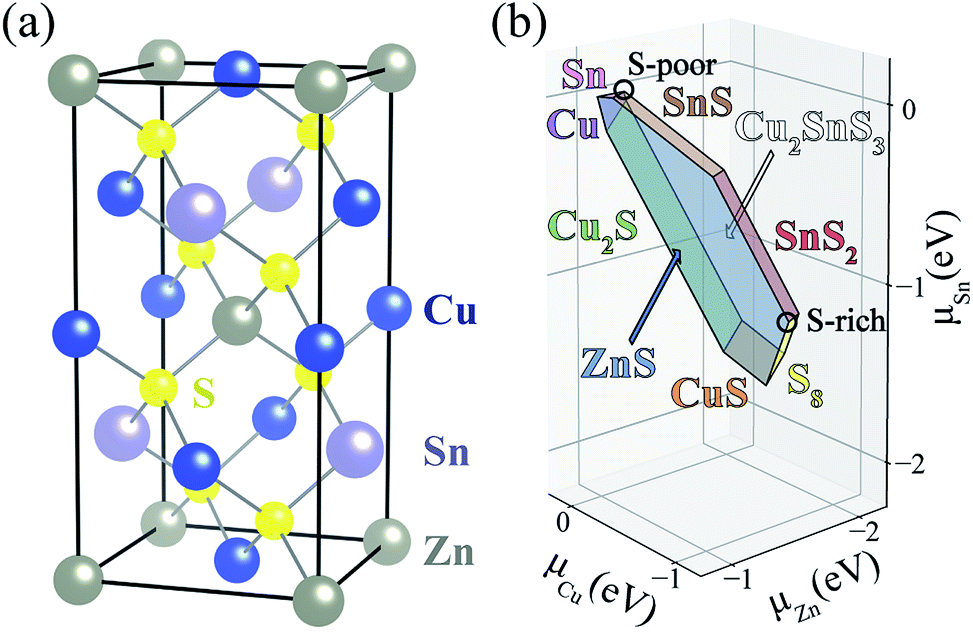 | ||
| Fig. 1 (a) Atomic structure and (b) phase diagram of CuZnSnS4 in chemical potential space, where μi = 0 represent element i in its standard state. Blue, gray, purple and yellow balls represent Cu, Zn, Sn, and S atoms, respectively. | ||
Thus, it is important to identify dominant recombination centers and to control their concentrations. According to Shockley–Read–Hall (SRH) statistics,16,17 a deep level in the band gap of a semiconductor acts as an efficient recombination channel that facilitates the sequential capture of minority and majority carriers. In addition to deep thermodynamic charge transition levels, large lattice distortions are required to achieve fast recombination rates.3,18 However, due to the strong interactions between an impurity and a host material, it is hard to predict the properties (charge transition level and lattice distortion) of impurities a priori or to find general trends in various host materials. Identification of recombination centers has relied on individual experimental or theoretical studies. If a simple criterion existed, then we could identify detrimental defects limiting the efficiency more easily and screen candidate optoelectronic materials more efficiently.
In this work, we argue that defects in semiconductors involving heavy post-transition metals are likely to act as fast non-radiative recombination centers not only due to their deep-level nature but also the large lattice distortions that accompany a change in oxidation state. As a representative case, we study the native point defects in CZTS containing multivalent ions of Sn and Cu. Through analysis of carrier capture rates from first-principles, we find that the dominant non-radiative recombination centers (VS, VS–CuZn and SnZn) are associated with Sn 5s2 lone-pair configurations. These defects produce deep donor levels due to the Sn double reduction, and the recombination processes involve large structure distortions because of the change in the ionic radius of Sn during the carrier capture. We expect to find similar behaviour for other lone pair cations including Bi and Sb.
Here, we use the notion XYq for a defect where X is the species (e.g. Cu, Zn, Sn, S or V for a vacancy), Y is the lattice site, and q is the charge state if specified. For example, VS represents the sulfur vacancy and SnZn is Sn-on-Zn antisite. Defect complexes are represented by symbols connected by a dash as in VS–VCu.
Methods
Non-radiative carrier capture
The phenomenon of carrier capture in semiconductors via multiphonon emission has been extensively studied following pioneering work by Huang and Rhys,19 and Henry and Lang.20 The initial excited state of system, for example, a positively charged donor (D+) with an electron in the conduction band (e−), vibrates around the equilibrium geometry. Owing to the electron–phonon coupling, the deformation of the structure causes the electronic energy level of a state localized around the defect to oscillate. As the defect level approaches the conduction band, the probability for the defect to capture an electron increases significantly. When an electron is captured, the donor becomes neutral (D0) and relaxes to a new equilibrium geometry by emitting multiple phonons as shown in Fig. 2. To describe and predict this process, quantitative accounts of the electronic and atomic structures as well as the vibrational properties of the defect are essential.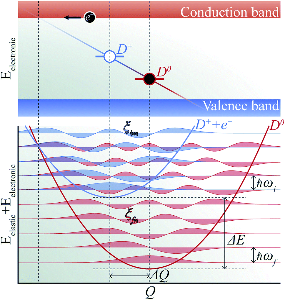 | ||
| Fig. 2 Schematic of non-radiative electron (e−) capture by a positively charged defect (D+) turning into the neutral defect (D0) in band diagram (upper panel) following Henry and Lang (ref. 20). The electron (black circle) is captured by the empty level (blue line) crossing the conduction band due to the thermal vibration of local geometry. The diagonal line represents evolution of the electronic energy level as the local geometry (Q) vibrates. The occupied level (red line) has a lower electronic energy due to the change in the equilibrium geometry (ΔQ). Configuration coordinate diagram (lower panel) for the same process shows potential energy surfaces of D+ + e− (blue curve) and D0 (red curve). The vibrational wave functions (ξim and ξfn, see the text) are shown in lighter shades. | ||
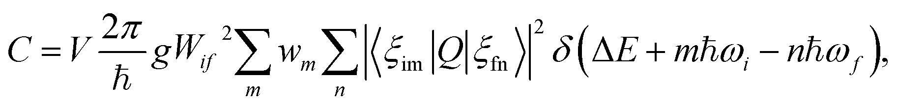
Recently, approaches have been developed for first-principles calculations of capture rates within a certain set of approximations.21,22 We have adopted a one-dimensional configuration coordinate for the effective vibrational wave function and the static coupling theory for electron-phonon coupling matrix elements as proposed by Alkauskas et al.22,23
We described the degree of deformation using a one-dimensional configuration coordinate Q defined by
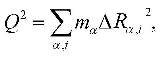 | (1) |
 | (2) |
The Coulomb interaction at temperature T between a carrier with charge q and a defect in a charge state Q is accounted by the Sommerfeld factor 〈s〉;24,25
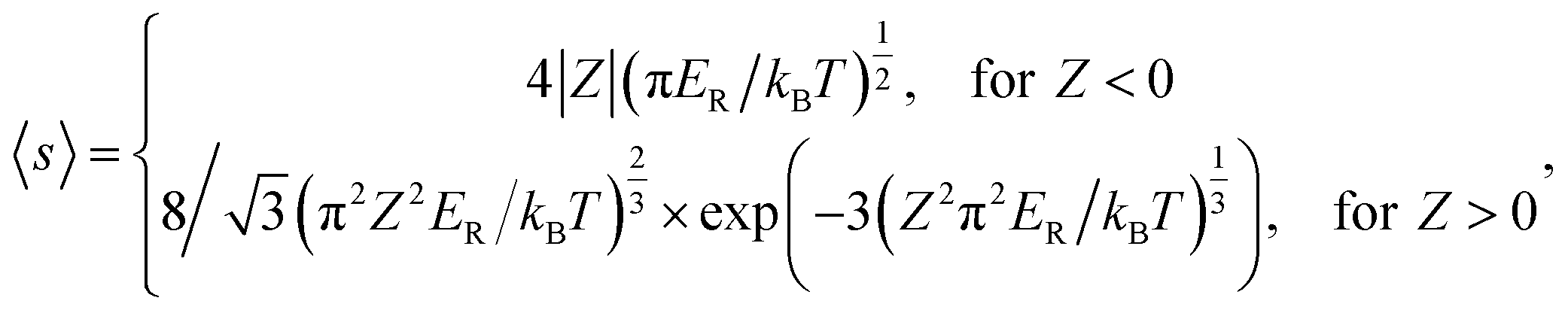 | (3) |
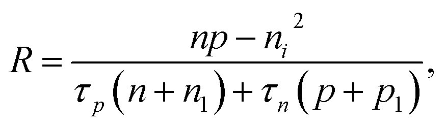
Based on the principle of detailed balance, the steady-state recombination rate R via a defect with electron-capture cross section σn and hole-capture cross section σp is given by16,17
 | (4) |
 | (5) |
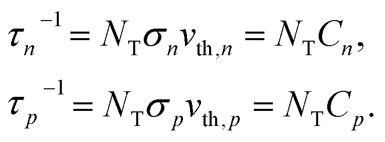
Here, n, p and NT denote concentrations of electrons, holes and defects, respectively. n1 and p1 represent the densities of electrons and holes, respectively, when the Fermi level is located at the trap level. The thermal velocities of electrons 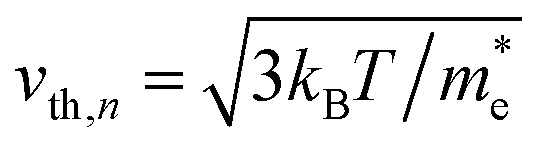 and holes
 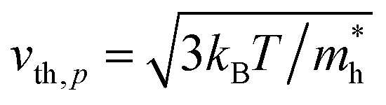 are calculated from the effective masses of electron
  and hole
  in the electronic band structure. Cn and Cp are the capture coefficients for electron and hole, respectively. Finally, the Shockley–Read–Hall recombination coefficient A is given by
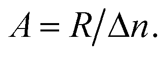 | (6) |
We assume an excess carrier concentration Δn = 1 × 1014 cm−3, which results in an open-circuit voltage VOC of 0.9 V. The Shockley–Read–Hall coefficient is not sensitive to the excess carrier concentration as long as Δn is much lower than the majority carrier concentration.
Electronic structure theory
The atomic and electronic structure of defects were calculated from first-principles within the framework of density functional theory (DFT).26,27 We employed the projector-augmented wave (PAW) method28 and the hybrid exchange-correlation functional of Heyd–Scuseria–Ernzerhof (HSE06),29 as implemented in VASP.30 The wave functions were expanded in plane waves up to an energy cutoff of 380 eV. A Monkhorst–Pack k-mesh31 with a grid spacing less than 2π × 0.03 Å−1 was used for Brillouin zone integration. The atomic coordinates were optimized until the residual forces were less than 0.02 eV Å−1. The lattice vectors were relaxed until stress was below 0.5 kbar. For defect formation, a 2 × 2 × 1 supercell expansion (64 atoms) of the conventional cell was employed.We calculated the formation energy ΔEform(Dq) of a defect D in the charge state q which is given by32
 | (7) |
Results and discussion
Equilibrium phase diagram
A challenge to achieving high efficiency from kesterite thin-film solar cell is to synthesize homogeneous CZTS without unintentional formation of secondary phases.15,36–39 The thermodynamic chemical potential μ of each element depends on the growth environment including partial pressures and temperature. We compare the DFT total energies of CZTS and its competing phases in the chemical potential space (Fig. 1(b)), showing the range of chemical potentials that favors the formation of CZTS, using CPLAP.40 The narrow range and complex shape of the phase diagram implies that it is hard to get a single-phase and homogeneous CZTS sample without the secondary phases. Even ‘pure’ CZTS is expected to contain an equilibrium population of point defects whose concentrations are controlled by the chemical potentials. We calculate the formation energies of the native defects under S-poor and S-rich conditions depicted in the phase diagram (Fig. 1(b)).S-poor growth environment
Under S-poor conditions, which could be realized by annealing in a low sulfur partial pressure, the most dominant native defects are CuZn and ZnCu antisites which are shallow and responsible for the p-type behaviour with a Fermi level close to the valence band (see Fig. 3(a)). At the Fermi level of 0.22 eV determined self-consistently, we predict high concentrations of VS (1.3 × 1016 cm−3), VS–CuZn (3.0 × 1017 cm−3) and SnZn (1.1 × 1018 cm−3). Here, we assume the growth and annealing temperature of 853 K resulting in defect populations. The operating temperature of a solar cell is a complex function of a level of irradiation, wind speed, humidity, and mounting type.41 We assumed a typical operating temperature of 330 K to equilibrate the Fermi level. | ||
| Fig. 3 Calculated formation energies of native defects in CZTS (a) under S-poor conditions and (b) under S-rich conditions. The self-consistent Fermi level resulting from the equilibrium defect population is shown as a vertical black dashed line. The top of valence band is set to 0 eV, while the bottom of conduction band is 1.46 eV. | ||
Previously, we have shown that VS can act as an efficient non-radiative recombination center in CZTS.42 However, for electron capture, VS needed to be activated. Firstly, as the ground state of V0S involving Sn(II) is neutral and produces a state resonant within the valence band, thermal excitation is required to access VS+. As shown in Fig. 4a, the hole capture barrier for VS+ is so high that the thermal motion can not overcome it. Instead, the optical absorption can trigger the vertical transition from VS+ to VS2+, which corresponds to Sn(III) to Sn(IV) oxidation.
 | ||
| Fig. 4 Configuration coordinate diagrams for (a) VS (2+/1+), (b) VS–CuZn (0/1+), (c) SnZn (2+/1+) and (d) SnZn (1+/0). The dot represents the formation energy calculated by DFT, and the line is a quadratic fit to the change in energy as the structure is distorted along the configuration coordinate. Q defines a pathway between the minimum-energy structure for each charge state. | ||
Here, we find that VS can also be activated by forming a defect complex with CuZn. In (VS–CuZn)0, the electronic wave function is localized around the Sn 5s lone-pair orbital similar to that of VS1+ (Fig. 5(a) and (b)), suggesting that the ionized acceptor CuZn1− ionizes the neutral donor V0S. Thus, Sn(III) becomes the ground-state electronic configuration in the neutral VS–CuZn complex, indicating, unlike the isolated VS, thermal excitation is not necessary.
 | ||
| Fig. 5 Charge density of the lowest unoccupied Kohn–Sham orbitals associated with (a) VS1+, (b) neutral (VS–VCu)0 and (c) SnZn1+. The black and orange balls represent VS and CuZn, respectively. | ||
We further find that optical excitation is not required for hole capture by the VS–CuZn complex. As a stronger Coulomb force binds the negatively charged acceptor CuZn1−, the formation energy difference between Sn(III) and Sn(IV) is reduced in the VS–VCu complex (Fig. 4(b)). Accordingly, the reduced barrier for hole capture facilitates carrier recombination without optical excitation. The subsequent electron capture process will be fast due to the negligible energy barrier (see Fig. 4(b)). The VS–VCu complex shows similar behavior, but its concentration is low under standard growth conditions.
We also examine recombination pathways via the donor levels of SnZn. Fig. 5(c) shows the defect charge density of SnZn is well localized around the Sn lone pair, suggesting the transitions involving Sn reduction and oxidation could trigger the carrier recombination similar to those in VS and VS–CuZn. The recombination path involving the double donor level SnZn(2+/1+) has a relatively high electron capture barrier of 0.23 eV (Fig. 4(c) and Table 1). On the other hand, SnZn(1+/0) – corresponding to the transition between Sn(III) and Sn(II) – has a smaller energy barrier of 0.05 eV, implying a faster recombination process.
| Defect | N T (cm−3) | σ (cm2) | E t (eV) | E b (meV) | A (s−1) | ||||
|---|---|---|---|---|---|---|---|---|---|
| S-poor | S-rich | n | p | n | p | S-poor | S-rich | ||
| VS–CuZn (+/0) | 3.0 × 10¹⁷ | 1.2 × 10¹² | 1.5 × 10⁻¹² | 8.4 × 10⁻¹⁴ | 0.24 | 9 | 190 | 9.8 × 10¹² | 3.81 × 10⁷ |
| SnZn (2+/1+) | 1.1 × 10¹⁸ | 3.3 × 10¹⁴ | 1.5 × 10⁻¹⁴ | 3.2 × 10⁻¹⁵ | 0.60 | 230 | 5 | 4.8 × 10¹¹ | 1.4 × 10⁸ |
| SnZn (1+/0) | 1.8 × 10¹² | 6.7 × 10⁸ | 5.5 × 10⁻¹³ | 5.5 × 10⁻¹⁵ | 0.87 | 54 | 184 | 2.7 × 10⁷ | 1.0 × 10⁴ |
| CuSn (2−/1−) | 2.7 × 10⁸ | 6.7 × 10¹¹ | 2.6 × 10⁻³⁴ | 1.3 × 10⁻¹⁶ | 0.31 | 1693 | 427 | 2.0 × 10⁻¹⁸ | 4.9 × 10⁻¹⁵ |
In Fig. 6(a), we present the capture cross section calculated within the static coupling approximation.22 VS–VCu and SnZn can be classified as a giant electron trap whose electron capture cross section (∼104 Å2) far exceeds the size of its atomic structure.18 The calculated capture cross sections of the native defects in CZTS are orders of magnitudes larger than extrinsic transition metal impurities in silicon solar cells including Ti, V, Cr, Mo, Fe, Au and Zn whose cross sections range from 10−1 Å2 to 103 Å2.46,47 This analysis suggests that VS–CuZn and SnZn are the main sources of non-radiative recombination that limit the efficiency of CZTS solar cells (see Table 1). Note that due to the small energy barrier of VS–CuZn, the recombination is expected to be fast even at low temperature. At high temperature, the slight decrease in the capture cross section is attributed to the high Landau–Zener velocity;48 the faster the defect level crosses the conduction bands, the less likely the defect captures electrons. The calculated capture cross section of SnZn1+ is an order of magnitude higher than that of SnZn2+ (Fig. 6 and Table 1).
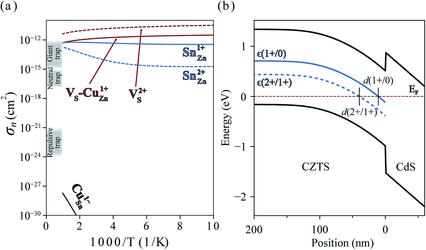 | ||
| Fig. 6 (a) Electron capture cross-sections of VS, VS–CuZn complex, SnZn, and CuSn. Gray shades represent the typical orders of magnitude of cross sections of giant, neutral and repulsive traps.18 (b) Band diagram of CZTS/CdS heterojunction. The solid and dashed blue curves represent the single ε(1+/0) and double donor levels ε(2+/1+) of SnZn, respectively. d(q1/q2) is defined by the distance from the interface where the charge transition levels of SnZnε(q1/q2) equals the Fermi level EF (red dashed line). The band diagram and d(2+/1+) = 40 nm are obtained by solving the Poisson–Boltzmann equation using https://pythonhosted.org/eq_band_diagram. | ||
In an operating solar cell, the recombination rate due to SnZn may depend on the spatial position because the distance from the interface between CZTS and CdS determines the Fermi level (electronic band bending) and, hence, the charge state of SnZn. In the undepleted region (d > d(2 +/1+)) in Fig. 6(b)), most of SnZn is in the form of +2 charge state which is a slower recombination channel. However, in the depletion region ((d < d(2 +/1+)), SnZn favors a +1 charge state which has much larger capture cross section. In this case, a recombination pathway is activated by band bending in a photovoltaic device.
S-rich growth environment
Under S-rich conditions, the formation of VS and VS–CuZn is strongly suppressed (see Fig. 3(b)). We associate this with the experimentally observed increase in VOC under a high S partial pressure during the annealing of a photovoltaic device.49 However, even under S-rich conditions, a considerable concentration of SnZn is still expected, which can limit the lifetime of carriers to below 7.1 ns (see Table 1). This shows good agreement with the reported photoluminescence (PL) decay times of kesterite materials which range from 1 ns to 10 ns.9,50 Moreover, the electron paramagnetic resonance (EPR) signal in CZTS51 supports the existence partially oxidized Sn(III) with an unpaired electron (5s1), which is the active state in the proposed recombination pathways.Inert-pair effect
The heavy post-transition metals (elements in groups 13, 14, 15 and 16) often exhibit oxidation states two less than the group valency, referred to as the inert-pair effect. The inert-pair effect is explained by the insufficient screening by d10 electrons resulting in the s2 lone-pair electrons tightly bound to the ion.52–55 However, the role of the inert-pair effect on the properties of defects in semiconductors has not been fully explored.Thus, the inert-pair effect in Sn is responsible for both the deep charge transition levels and the large lattice distortion of VS, VS–CuZn and SnZn, which make them efficient non-radiative recombination centers. Similarly, we find the deep acceptor level of CuSn owing to the oxidation of Cu. However, the electron capture rates by CuSn (1−/2−) are low (Table 1). The multivalency of Cu is due to the change in the occupation of 3d orbital: from 3d10 in Cu(I) to 3d9 in Cu(II). Thus, the local relaxation after the oxidation is not significant. The small lattice distortion in CuSn produces an electron capture barrier above 1.6 eV, making capture unlikely (Fig. 6(a)).
Emergence of deep defects induced by the formation of lone pairs has also been reported in CIGS. Extrinsic dopants of Bi and Sb are deep in CuInSe2 due to the lone-pair s2 states.59 Han et al.60 have also found that the formation of lone pairs in amorphous oxide semiconductors, such as InGaZnO4 and ZnSnO3, is responsible for electron trapping.
While Sn reduction captures electrons, in lone-pair compounds whose cations, such as Tl(I), Pb(II) and Bi(III), have occupied s2 orbitals in the stoichiometric compounds, the oxidation of cations could capture holes. Several EPR measurements show that Pb(III) is responsible for the hole traps in lead halides.61–64
The efficiency and lifetime of optoelectronic devices can be severely damaged by a defect with fast non-radiative recombination. Stoneham18 suggests several characteristics of such killer centers, including: (1) defects producing many and closely spaced electronic levels; (2) defects with large lattice distortions. The first type can be directly related to the transition metal impurities with partially filled d orbitals (e.g. Ni in GaP). While a simple vacancy center was suggested as a candidate for the second-type,18 a wide variety of vacancies are not recombination centers in photovoltaic materials (e.g. VCu is a shallow acceptor in CZTS, and VI is a shallow donor in CH3NH3PbI3.) Because of the strong interaction between impurities and host materials, it is difficult to find a general trend of the properties of defects in the absence of detailed calculations. On the other hand, we find that the inert lone-pair of Sn is the origin of the large cross-section of an wide range of defects and not significantly altered by a specific configuration or an electronic state of the defect. Thus, we speculate that the inert-pair effect could likely cause killer centers with the ability to act as giant carrier traps in a broad range of semiconductors.
Many photovoltaic materials with band gaps close to the theoretical optimum of 1.3–1.5 eV (ref. 13) show poor performances; in particular a low VOC. The record efficiency of Cu2SnS3, whose band gap is around 1 eV, is still low (4.63%) even with the high current density JSC of 37.3 mA cm−2 mainly because of low VOC of 283 mV.65 The carrier lifetime of Cu2SnS3 was reported to be very short (0.1–10 ps).66 Sb2Se3 solar cells also exhibit low VOC with short carrier lifetime of 1.3 ns.67 The first light-to-electricity conversion efficiency of Cu3BiS3 solar cell (0.17%) has been achieved only recently with VOC of 190 meV,68 and, to our knowledge, a successful operation of CuBiS2 solar cell has not been reported. The presence of lone-pair cations is a common feature in these technologies.
Conclusion
The lone-pair effect associated with Sn is responsible for both the deep defect levels and large lattice distortions that facilitate rapid electron–hole recombination in the semiconductor Cu2ZnSnS4. By employing a first-principles approach to predict the defect levels, concentrations, and capture rates, we can distinguish between active and inactive defect centres. For a material grown under S-poor conditions, VS, VS–CuZn and SnZn act as dominant recombination centers, while SnZn limits the minority carrier lifetime under S-rich conditions. We propose that a similar mechanism could underpin the low performance of other emerging photovoltaic compounds. We emphasise the need for further experimental and theoretical investigation of defects in semiconductors composed of heavy post-transition metals to further evaluate the general role of the inert-pair effect on the non-radiative electron–hole recombination process.Conflicts of interest
There are no conflicts to declare.Acknowledgements
We acknowledge support from the Royal Society, the EPSRC (Grant No. EP/K016288/1), and the EU Horizon2020 Framework (STARCELL, Grant No. 720907). We are grateful to the UK Materials and Molecular Modeling Hub for computational resources, which is partially funded by EPSRC (EP/P020194/1). Via our membership of the UK's HEC Materials Chemistry Consortium, which is funded by EPSRC (EP/L000202), this work used the ARCHER UK National Supercomputing Service (http://www.archer.ac.uk). This work was also supported by a National Research Foundation of Korea (NRF) grant funded by the Korean government (MSIT) (No. 2018R1C1B6008728).Notes and references
- J. Nelson, The Physics of Solar Cells, Imperial College Press, London, UK, 2003 Search PubMed.
- J.-S. Park, S. Kim, Z. Xie and A. Walsh, Nat. Rev. Mater., 2018, 50, 797 Search PubMed.
- A. M. Stoneham, Rep. Prog. Phys., 2000, 44, 1251 CrossRef.
- T. Kirchartz and U. Rau, Adv. Energy Mater., 2018, 356, 1703385 CrossRef.
- M. Kumar and C. Persson, Int. J. Theor. Appl. Sci., 2013, 5, 1 CrossRef.
- M. Kumar, A. Dubey, N. Adhikari, S. Venkatesan and Q. Qiao, Energy Environ. Sci., 2015, 8, 3134 RSC.
- K. Kaur, N. Kumar and M. Kumar, J. Mater. Chem. A, 2017, 5, 3069 RSC.
- W. Wang, M. T. Winkler, O. Gunawan, T. Gokmen, T. K. Todorov, Y. Zhu and D. B. Mitzi, Adv. Energy Mater., 2013, 4, 1301465 CrossRef.
- C. Yan, J. Huang, K. Sun, S. Johnston, Y. Zhang, H. Sun, A. Pu, M. He, F. Liu, K. Eder, L. Yang, J. M. Cairney, N. J. Ekins-Daukes, Z. Hameiri, J. A. Stride, S. Chen, M. A. Green and X. Hao, Nat. Energy, 2018, 1, 15015 Search PubMed.
- D. A. R. Barkhouse, O. Gunawan, T. Gokmen, T. K. Todorov and D. B. Mitzi, Prog. Photovolt: Res. Appl., 2011, 20, 6 CrossRef.
- T. K. Todorov, J. Tang, S. Bag, O. Gunawan, T. Gokmen, Y. Zhu and D. B. Mitzi, Adv. Energy Mater., 2012, 3, 34 CrossRef.
- L. Grenet, M. A. A. Suzon, F. Emieux and F. Roux, ACS Appl. Energy Mater., 2018, 1, 2103 CrossRef CAS.
- W. Shockley and H. J. Queisser, J. Appl. Phys., 1961, 32, 510 CrossRef CAS.
- S. Rühle, Sol. Energy, 2016, 130, 139 CrossRef.
- S. K. Wallace, D. B. Mitzi and A. Walsh, ACS Energy Lett., 2017, 2, 776 CrossRef CAS.
- R. N. Hall, Phys. Rev., 1952, 87, 387 CrossRef CAS.
- W. Shockley and J. W. T Read, Phys. Rev., 1952, 87, 835 CrossRef CAS.
- A. M. Stoneham, Theory of Defects in Solids, Oxford University Press, Oxford, UK, 1975 Search PubMed.
- K. Huang and A. Rhys, Proc. R. Soc. A, 1950, 204, 406 CAS.
- C. H. Henry and D. V. Lang, Phys. Rev. B, 1977, 15, 989 CrossRef CAS.
- L. Shi and L.-W. Wang, Phys. Rev. Lett., 2012, 109, 245501 CrossRef PubMed.
- A. Alkauskas, Q. Yan and C. G. Van de Walle, Phys. Rev. B, 2014, 90, 075202 CrossRef.
- A. Alkauskas, M. D. McCluskey and C. G. Van de Walle, J. Appl. Phys., 2016, 119, 181101 CrossRef.
- R. Pässler, Phys. Status Solidi B, 1976, 78, 625 CrossRef.
- P. T. Landsberg, Recombination in Semiconductors, Cambridge University Press, Cambridge, UK, 2009 Search PubMed.
- P. Hohenberg and W. Kohn, Phys. Rev., 1964, 136, B864 CrossRef.
- W. Kohn and L. J. Sham, Phys. Rev., 1965, 140, A1133 CrossRef.
- P. E. Blöchl, Phys. Rev. B, 1994, 50, 17953 CrossRef.
- J. Heyd, G. E. Scuseria and M. Ernzerhof, J. Chem. Phys., 2003, 118, 8207 CrossRef CAS.
- G. Kresse and D. Joubert, Phys. Rev. B, 1999, 59, 1758 CrossRef CAS.
- H. J. Monkhorst and J. D. Pack, Phys. Rev. B, 1976, 13, 5188 CrossRef.
- C. Freysoldt, B. Grabowski, T. Hickel, J. Neugebauer, G. Kresse, A. Janotti and C. G. Van de Walle, Rev. Mod. Phys., 2014, 86, 253 CrossRef.
- C. Freysoldt, J. Neugebauer and C. G. Van de Walle, Phys. Rev. Lett., 2009, 102, 016402 CrossRef PubMed.
- Y. Kumagai and F. Oba, Phys. Rev. B, 2014, 89, 195205 CrossRef.
- SC-FERMI, https://github.com/jbuckeridge/sc-fermi, accessed: 2019-01-03.
- J. J. S. Scragg, P. J. Dale, L. M. Peter, G. Zoppi and I. Forbes, Phys. Status Solidi B, 2008, 245, 1772 CrossRef CAS.
- S. Chen, X. G. Gong, A. Walsh and S.-H. Wei, Appl. Phys. Lett., 2010, 96, 021902 CrossRef.
- A. J. Jackson and A. Walsh, J. Mater. Chem. A, 2014, 2, 7829 RSC.
- M. Dimitrievska, A. Fairbrother, E. Saucedo, A. Perez-Rodriguez and V. Izquierdo-Roca, Sol. Energy Mater. Sol. Cells, 2016, 149, 304 CrossRef CAS.
- J. Buckeridge, D. O. Scanlon, A. Walsh and C. R. A. Catlow, Comput. Phys. Commun., 2014, 185, 330 CrossRef CAS.
- E. Skoplaki, A. G. Boudouvis and J. A. Palyvos, Sol. Energy Mater. Sol. Cells, 2008, 92, 1393 CrossRef CAS.
- S. Kim, J.-S. Park and A. Walsh, ACS Energy Lett., 2018, 3, 496 CrossRef CAS.
- S. Chen, J.-H. Yang, X. G. Gong, A. Walsh and S.-H. Wei, Phys. Rev. B, 2010, 81, 245204 CrossRef.
- S. B. Zhang, S.-H. Wei, A. Zunger and H. Katayama-Yoshida, Phys. Rev. B, 1998, 57, 9642 CrossRef CAS.
- A. Walsh and A. Zunger, Nat. Mater., 2017, 50, 797 Search PubMed.
- D. Macdonald and L. J. Geerligs, Appl. Phys. Lett., 2004, 85, 4061 CrossRef CAS.
- A. R. Peaker, V. P. Markevich, B. Hamilton, G. Parada, A. Dudas, A. Pap, E. Don, B. Lim, J. Schmidt, L. Yu, Y. Yoon and G. Rozgonyi, Phys. Status Solidi A, 2012, 209, 1884 CrossRef CAS.
- C. Zener, Proc. R. Soc. A, 1932, 137, 696 CrossRef.
- Y. Ren, N. Ross, J. K. Larsen, K. Rudisch, J. J. S. Scragg and C. Platzer-Björkman, Chem. Mater., 2017, 29, 3713 CrossRef CAS.
- C. J. Hages, A. Redinger, S. Levcenko, H. Hempel, M. J. Koeper, R. Agrawal, D. Greiner, C. A. Kaufmann and T. Unold, Adv. Energy Mater., 2017, 7, 1700167 CrossRef.
- C. Chory, F. Zutz, F. Witt, H. Borchert and J. Parisi, Phys. Status Solidi C, 2010, 7, 1486 CrossRef CAS.
- N. V. Sidgwick and H. M. Powell, Proc. R. Soc. London, Ser. A, 1940, 176, 153 CAS.
- R. J. Gillespie and R. S. Nyholm, Q. Rev., Chem. Soc., 1957, 11, 339 RSC.
- L. Shimoni-Livny, J. P. Glusker and C. W. Bock, Inorg. Chem., 1998, 37, 1853 CrossRef CAS.
- A. Walsh, D. J. Payne, R. G. Egdell and G. W. Watson, Chem. Soc. Rev., 2011, 40, 4455 RSC.
- K. Biswas, S. Lany and A. Zunger, Appl. Phys. Lett., 2010, 96, 201902 CrossRef.
- D. Han, Y. Y. Sun, J. Bang, Y. Y. Zhang, H.-B. Sun, X.-B. Li and S. Zhang, Phys. Rev. B, 2013, 87, 155206 CrossRef.
- D. L. Dexter, C. C. Klick and G. A. Russell, Phys. Rev., 1955, 100, 603 CrossRef CAS.
- J.-S. Park, J.-H. Yang, K. Ramanathan and S.-H. Wei, Appl. Phys. Lett., 2014, 105, 243901 CrossRef.
- W. H. Han and K. J. Chang, Phys. Rev. Appl., 2016, 6, 044011 CrossRef.
- M. Iwanaga, M. Shirai, K. Tanaka and T. Hayashi, Phys. Rev. B, 2002, 66, 064304 CrossRef.
- I. A. Shkrob and T. W. Marin, J. Phys. Chem. Lett., 2014, 5, 1066 CrossRef CAS PubMed.
- D. Cortecchia, J. Yin, A. Bruno, S.-Z. A. Lo, G. G. Gurzadyan, S. Mhaisalkar, J.-L. Brédas and C. Soci, J. Mater. Chem. C, 2017, 5, 2771–2780 RSC.
- S. Colella, M. Todaro, S. Masi, A. Listorti, D. Altamura, R. Caliandro, C. Giannini, E. Carignani, M. Geppi, D. Meggiolaro, G. Buscarino, F. De Angelis and A. Rizzo, ACS Energy Lett., 2018, 3, 1840–1847 CrossRef CAS.
- M. Nakashima, J. Fujimoto, T. Yamaguchi and M. Izaki, Appl. Phys. Express, 2015, 8, 042303 CrossRef.
- L. L. Baranowski, K. McLaughlin, P. Zawadzki, S. Lany, A. Norman, H. Hempel, R. Eichberger, T. Unold, E. S. Toberer and A. Zakutayev, Phys. Rev. Appl., 2015, 4, 044017 CrossRef.
- X. Wen, C. Chen, S. Lu, K. Li, R. Kondrotas, Y. Zhao, W. Chen, L. Gao, C. Wang, J. Zhang, G. Niu and J. Tang, Nat. Commun., 2018, 9, 2179 CrossRef PubMed.
- J. Li, X. Han, Y. Zhao, J. Li, M. Wang and C. Dong, Sol. Energy Mater. Sol. Cells, 2018, 174, 593 CrossRef CAS.
| This journal is © The Royal Society of Chemistry 2019 |