
Simultaneous enhancement in performance and UV-light stability of organic–inorganic perovskite solar cells using a samarium-based down conversion material†
Naveed Ur
Rahman
a,
Wasim Ullah
Khan
b,
Wenlang
Li
a,
Shaukat
Khan
b,
Javid
Khan
b,
Shizhao
Zheng
*a,
Tongtong
Su
a,
Juan
Zhao
 *a,
Matthew P.
Aldred
a and
Zhenguo
Chi
*a
*a,
Matthew P.
Aldred
a and
Zhenguo
Chi
*a
aPCFM Lab, GD HPPC Lab, Guangdong Engineering Technology Research Center for High-performance Organic and Polymer Photoelectric Functional Films, State Key Laboratory of Optoelectronic Material and Technologies, School of Chemistry, Sun Yat-sen University, Guangzhou 510275, PR China. E-mail: chizhg@mail.sysu.edu.cn; zhaoj95@mail.sysu.edu.cn; zshizhao@mail.sysu.edu.cn
bSchool of Chemistry, Sun Yat-sen University, Guangzhou 510275, PR China
First published on 20th November 2018
Abstract
Extending the spectral response from the ultraviolet (UV) to the visible-light range and enhancing the UV-light stability are two remaining challenges for the development of perovskite solar cells (PSCs). Lanthanide complexes show a broad absorption range in the UV region and can down convert UV-light into visible-light; thus, they are potentially able to improve the device performance of PSCs. Herein, we report the fabrication of PSCs with a novel samarium (Sm)-based down conversion nanomaterial, Sr2CeO4:Sm3+ (SCOS). In comparison to the control device without a SCOS layer, the SCOS-coated device shows an enhancement of 11.4% in photocurrent and 16.2% in average power conversion efficiency (PCE), due to the harvesting and re-emitting of UV-light in the visible range through the SCOS layer. Significantly, the SCOS-coated devices retain 50% of their initial PCE for 60 hours under continuous UV-light illumination and even after 60 days of storage under ambient environment conditions, whilst for the control device the longevity is 15 hours and 26 days, respectively. The results suggest that the SCOS layer makes an important contribution in terms of both enhanced photovoltaic performance and prolonged device stability by reducing photo-loss and photo-degradation.
Introduction
Organic–inorganic halide perovskite solar cells (PSCs) constitute an emerging top research area in photovoltaics, and have attracted tremendous research interest.1–6 In PSCs, perovskites are the most promising materials for next generation low-cost and highly efficient solar cells due to their remarkable optical and electronic properties, such as high light absorption coefficient (104–105 cm−1), high charge-carrier mobility, low exciton binding energy (≈50 meV) and long carrier diffusion length.7–11 To date, the power conversion efficiency (PCE) of perovskite solar cells has been improved from 3.8% (ref. 12) to 23.3% (ref. 13) by virtue of great advances made in materials and fabrication technologies, such as improved perovskite film quality and improved properties of charge transporting materials.14–17 However, the stability of PSCs under ambient environment and illumination conditions is compromised, representing a currently intractable challenge. Therefore, current research has been mainly focused on achieving the goal of long-term stability of PSCs in humid and open environments; however, the ultraviolet (UV)-light stability of PSCs is still of great importance.18–21 As is known, UV-light illumination involves the issue of decomposition of the perovskite layer, which is due to the presence of the methylammonium ion (CH3NH3+) in the materials22 and is also caused by oxygen vacancies and defects, degrading the PSC performance and stability.23–25 To overcome this problem of photodegradation, a number of approaches such as photo-anode modification,26–28 halogen ion doping,29–31 hole transporting materials (HTMs) design,32–35 and UV filter film usage36–38 have been proposed. However, these approaches have only resulted in partial improvement of performance and stability. On the other hand, with respect to the widely used hybrid lead halide perovskite materials, such as CH3NH3PbI3, they have a favorable direct bandgap (1.55 eV) for good absorption of light in the visible range.39 However, visible light only comprises 44% of the total incident light while 50% of the light lies in the UV and infrared ranges, which PSCs are unable to utilize, thus limiting the device performance of PSCs. In this regard, novel approaches enabling simultaneous improvement in the UV-light absorption and stability could be more intriguing and also in high demand.To meet these requirements, one promising approach is the utilization of down conversion materials, which have the ability of absorbing UV-light and re-emitting visible-light due to their 4f electronic structure.40–43 In addition, the introduction of down conversion materials can help in preventing UV-light from interacting with the perovskite layer, removing the load of spectral matching and decreasing thermalization losses in the device,44–47 showing potential to reduce the UV-light corrosion of the device and accordingly enhance the device stability. Meanwhile, the introduced down conversion layer can absorb all converted light, enhance charge-carrier transportation and reduce charge-carrier recombination,48–50 thus improving PSC performance. To date, a few down conversion materials, which are mostly lanthanide-based photoluminescent materials, have been employed in PSCs, leading to enhancement in either light harvesting or UV-light stability.51–54 For example, the introduction of a CeO2:Eu3+ nanophosphor51 endowed the PSCs with a 6.9% improvement in PCE compared to that of devices without the nanophosphor, while the efficiency was reduced by 32% after 50 min under UV irradiation. Another down conversion material Y2O3:Eu3+ was introduced into PSCs and resulted in a 5.9% increase in PCE, which decreased by 60% after 24 h of UV irradiation.53 Therefore, it is clear that it remains an important challenge to simultaneously improve the photovoltaic performance and UV-light stability of PSCs.54
In this work, a samarium (Sm)-based down conversion material, namely Sr2CeO4:Sm3+ (SCOS), was introduced into PSCs to increase the light harvesting efficiency and UV-light stability. The SCOS nanophosphors converted UV light (283–400 nm) to visible light that matched well with the absorption of the perovskite material, thus helping to make full use of incident light for performance enhancement of PSCs. Importantly, the SCOS-coated devices show more excellent long-term stability under UV-light irradiation and open environment conditions, demonstrating the novelty of the multifunctional SCOS material. To the best of our knowledge, this is the first study employing a samarium-based down conversion material in PSCs.
Experimental
Materials
All solvents and reagents were commercially available, pure and used without further purification. Cerium oxide (CeO2), samarium oxide (Sm2O3), and strontium carbonate (SrCO3) were purchased from Aladdin. Lead(II) iodide, dimethyl sulfoxide, lithium bis(trifluoromethylsulphonyl) imide (Li-TFSI), 4-tert-butylpyridine (TBP) and titanium isopropoxide were purchased from Aldrich. Methylammonium iodide and spiro-OMeTAD were obtained from Xi'an Polymer Light Technology Co. Ltd.; acetylacetonate, N,N-dimethylformamide, ethanol and chlorobenzene were from Sinopharm. Details of device fabrication and characterization are provided in the ESI.†Synthesis and characterization of samarium nanophosphors
Samarium (Sm)-based down conversion materials (SCOS nanophosphors) were synthesized via a solid-state reaction method. The reactants were as follows: SrCO3 (A.R. grade), Na2CO3 (A.R. grade), Sm2O3 (99.99%) and Ce2O3 (99.99%). Materials in designed stoichiometric composition were thoroughly mixed and ground by using a pestle in an agate mortar. Subsequently, the well-ground mixture was transferred to an alumina crucible and calcined at 1200 °C for 3 h in an air atmosphere. Finally, the obtained SCOS nanophosphors were ground again and used for further measurements. The morphology and structure of the SCOS and PSCs (surface and cross sectional) and the energy-dispersive X-ray spectroscopy (EDS) spectrum of the SCOS were investigated by scanning electron microscopy (SEM, FEI, Quanta450 FEG) and X-ray diffraction (XRD, Bruker D8 Advance with Cu Kα radiation), as well as high resolution transmission electron microscopy (HRTEM) and selected area electron diffraction (SAED) analysis, which were performed using an FEI Tecnai G2 Spirit, and UV-vis absorption spectroscopy, which was carried out using a UV-vis spectrometer (Hitachi U-3900). The photoluminescence (PL) spectra of the SCOS nanocrystals were examined using a fluorescence spectrophotometer (RF-5301PC). The roughness of the films was characterized by atomic force microscopy (AFM, Bruker Multimode 8 SPM system). X-ray photoelectron spectroscopy (XPS) measurements were performed using an ESCALAB 250Xi (Thermo Fisher Scientific). Optical diffuse reflectance measurements were performed at room temperature on a UV-visible-NIR spectrometer (Carry-5000) to obtain diffuse reflectance spectra (DRS). Electrochemical characterization was carried out using an electrochemical workstation, VMP300 (Bio-Logic), at a scan rate of 100 mV s−1 with tetrabutylammoniumhexafluorophosphate (TBAPF6, 0.1 M) in dichloromethane as the electrolyte. Cyclic voltammetry (CV) measurements were conducted using platinum as the counter electrode, and a Ag/AgCl electrode as the reference electrode (versus ferrocene (Fc/Fc+)).Results and discussion
Samarium-based down conversion material
HRTEM (Fig. 1a) shows an inter-planar lattice spacing of 0.37 nm corresponding to the (111) crystal planes of the SCOS crystals, while good crystallinity can also be evidenced by SAED (Fig. 1b). The XRD patterns of the SCOS materials (Fig. 1c) demonstrate the formation of orthorhombic Sr2CeO4:Sm3+ nanoparticles, indicating that the SCOS material is crystalline.55 The results of the given samples match well with those of the Joint Committee on Powder Diffraction Standards, JCPDS card no. 50-0115.56 The EDS mapping spectra were recorded to determine the existence of the host (Sr, Ce, and O) and dopant (Sm) elements (Fig. S1†). Further evidence for the elemental composition of Sr2CeO4:Sm3+ was provided by XPS measurements (Fig. S2 and Table S1†), showing a surface elemental composition of O, Ce, Sm and Sr. When SCOS nanoparticles were dispersed in different solvents (Fig. S3†), a stable suspension was found in 2-methoxy ethanol solution, helping in the formation of uniform thin films. The SEM of the SCOS film demonstrates its uniform surface morphology (Fig. 1d).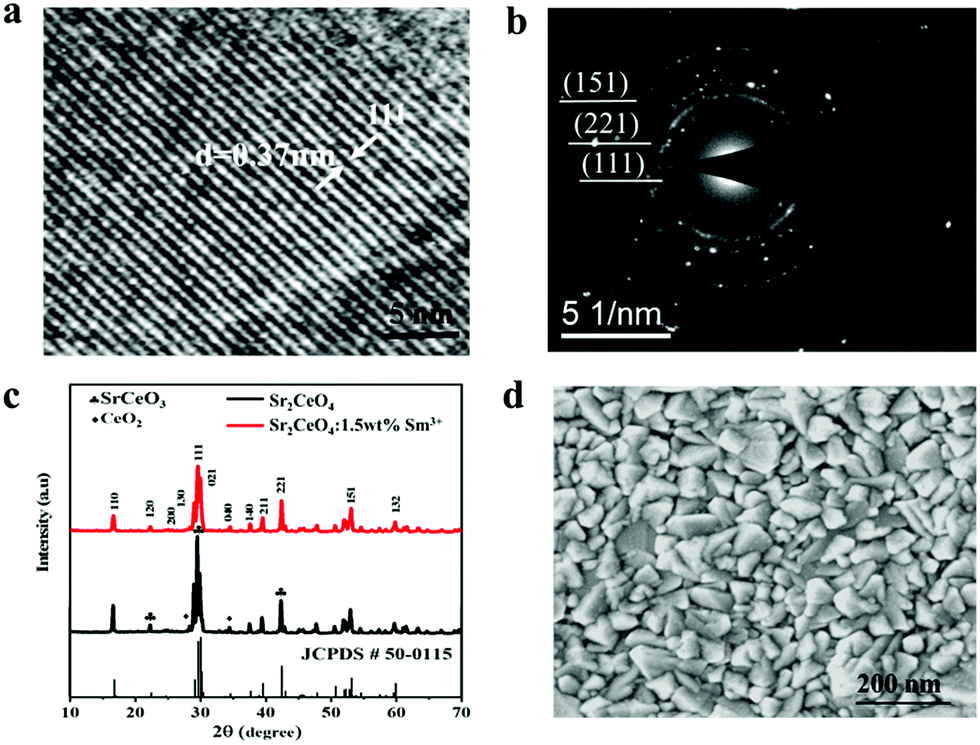 | ||
| Fig. 1 (a) HRTEM, (b) SAED and (c) XRD patterns of the SCOS nanoparticles. (d) SEM image of a SCOS film. | ||
The Sm3+ concentration is assumed to have an important influence on the UV absorption and PL properties of the SCOS films. The UV-vis absorption spectra of SCOS thin layers with different Sm3+ concentrations (0.5 wt%, 1.0 wt%, 1.5 wt%, and 2.0 wt%) are shown in Fig. 2a. The SCOS films show a UV absorption band in the range of 283–400 nm covering a broad range of incident UV-light. As shown, there is an increased tendency of absorption with increasing Sm3+ content in the SCOS layers, and the absorption reaches a maximum when the Sm3+ concentration is 1.5 wt%. However, further increase of Sm3+ concentration leads to gradual diminution of the Sm3+ band as cross relaxation (concentration quenching) becomes dominant.57 These results are in agreement with the transmission spectrum results of the SCOS layers, depicting high light absorption for the 1.5% Sm3+ doped layer in the UV region (Fig. S4†). Fig. 2b displays the PL emission spectra of the Sm3+ doped SCOS layers using 350 nm excitation, which consist of emission peaks at 480, 564, 608 and 647 nm. The peak at 480 nm is attributed to Ce4+–O2− charge transfer, while typical Sm3+ emission peaks induced by 4G5/2 → 6H5/2 (564 nm), 4G5/2 → 6H7/2 (608 nm) and 4G5/2 → 6H9/2 (647 nm) transitions from the excited level to the ground level are clearly observed.54 The peak with the highest intensity is at 608 nm, originating from the typical 4G5/2 → 6H7/2 transition for Sm3+.58 These results indicate that the SCOS film down converts the UV-light into low energy photons, which are well matched with the absorption range of perovskite materials. It is found that the PL emission intensity of 4G5/2 → 6H7/2 increases with the increase of Sm3+ concentration up to 1.5 wt%, where it reaches a maximum range. A further rise in Sm3+ concentration (2.0 wt%) brings about a decrease in the PL intensity because of concentration quenching of Sm3+ ions, which easily occurs due to the cross-relaxation effect.57 Based on the above observations of absorption, transmission and emission spectra, 1.5 wt% Sm3+ doped nanophosphors show the best spectral response and, therefore, are considered suitable for achieving high photovoltaic performance. The energy band gap (Eg) of the samarium-based nanophosphors was determined to be 3.03 eV from the DRS measurement (Fig. S5†) according to the Kubelka–Munk function.59,60 The valence band was estimated to be 6.96 eV from the CV characteristic (Fig. S6†),61 and then the conduction band was found to be 3.93 eV.
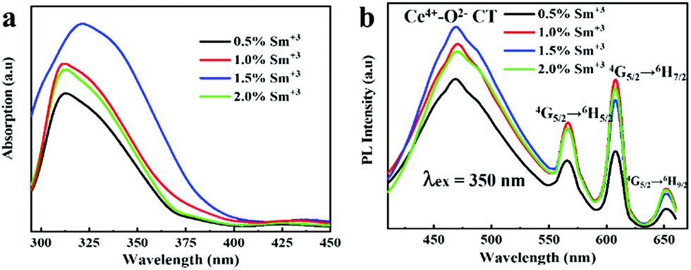 | ||
| Fig. 2 (a) Absorption and (b) PL emission spectra of SCOS films with various Sm3+ doping concentrations. | ||
Photovoltaic performance of the PSCs
To investigate the effect of the SCOS layer, the UV-vis absorption spectra of two samples including FTO/c-TiO2/SCOS/(CsFAMA)Pb(BrI)3 (SCOS sample) and FTO/c-TiO2/(CsFAMA)Pb(BrI)3 (control sample) were compared, and are shown in Fig. S7.† In comparison to the control sample without the SCOS layer, the SCOS sample exhibits obviously stronger absorption in the visible region from 450 to 850 nm, which is helpful for performance improvement of the PSCs. Motivated by the good crystallinity and intense absorption of the perovskite (CsFAMA)Pb(BrI)3 thin film grown on the SCOS layer, PSC devices were fabricated to evaluate their photovoltaic properties. The PSCs were fabricated with the following device configuration (Fig. 3a): FTO/c-TiO2/SCOS/(CsFAMA)Pb(BrI)3/spiro-OMeTAD/Au. The thicknesses of the FTO, compact TiO2 (c-TiO2), SCOS layer, perovskite layer, spiro-OMeTAD HTM and Au electrode, which are 580 nm, 30 nm, 150 nm, 490 nm, 184 nm and 124 nm, respectively, are determined by the cross sectional SEM result (Fig. S8†). The cross-sectional SEM also indicates the uniform thickness, flat surfaces and strong interface binding of all the deposited layers, which favor high device performance. Meanwhile, devices without the SCOS layer were fabricated in the same way as the control devices, and the other layers were maintained the same as they were in the SCOS devices. Fig. 3b shows the current density–voltage (J–V) curves of the optimized SCOS device and control device, and all the photovoltaic parameters including short-circuit current density (Jsc), open circuit voltage (Voc), fill factor (FF) and PCE are summarized in Table 1. For the control device, the Jsc, Voc and FF are equal to 21.22 mA cm−2, 1.02 V and 71.1%, respectively. Surprisingly, for the SCOS device, the Jsc, Voc and FF are found to be 23.65 mA cm−2, 1.05 V and 72.4%, respectively. Meanwhile, the average PCE calculated from 45 SCOS cells reaches up to 17.9%, while the average PCE from 45 control cells is 15.4% (Fig. 3c). As a result, the SCOS devices show an enhancement of 11.4% in photocurrent and 16.2% in average PCE. In comparison, the SCOS devices in this work present the best performance compared to previous perovskite solar cells based on various down conversion phosphor materials (Table S2†), most of which are europium ion (Eu3+)-based materials. As shown in Fig. 3d, the SCOS device presents a negligible hysteresis phenomenon when driven between forward and reverse scans. The reason is mainly associated with the morphological features of the perovskite layer, which can be supported by the SEM image of the perovskite film (Fig. S9†). As can be observed, the perovskite film coated on c-TiO2/SCOS is uniform and compact with large grain size, and no observable pinholes are shown, suggesting the presence of negligible defects and hence good perovskite film quality. Thereby, the presence of fewer defects is helpful in impeding charge accumulation and recombination at the interface region caused by ionic diffusion,62 thus restraining the strength of the hysteresis in the SCOS devices.63 Stabilized power output measurement is also carried out by holding the voltage at the maximum power point, as plotted in Fig. S10.† The control device achieved a steady-state PCE of 14.70% with a steady-state current density of 19.15 mA cm−2. Meanwhile, the SCOS-based device achieved a steady-state PCE of 17.21% with a steady-state current density of 21.45 mA cm−2, which is in good agreement with the small hysteresis and verifies the PCE from the J–V curves.64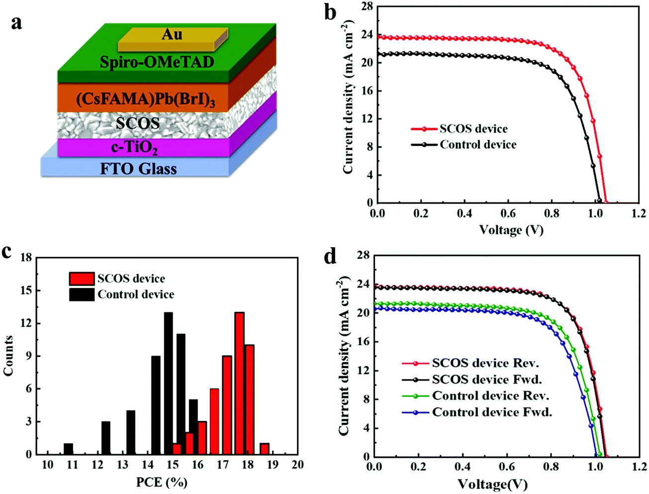 | ||
| Fig. 3 (a) Device structure of the SCOS devices. (b) J–V curves of the control and the SCOS PSC devices under simulated AM 1.5 illumination. (c) Statistical histogram of the efficiency for 45 control PSCs and 45 SCOS-based PSCs, representing 45 data points for each kind of device. (d) Forward and reverse scans of the control and the SCOS devices. | ||
| Device | Scan | J sc [mA cm−2] | V oc [V] | FF [%] | PCE [%] |
|---|---|---|---|---|---|
| Control | Reverse | 21.22 | 1.02 | 71.1 | 15.4 |
| Forward | 21.22 | 1.01 | 70.0 | 15.1 | |
| SCOS | Reverse | 23.65 | 1.05 | 72.4 | 17.9 |
| Forward | 23.51 | 1.04 | 72.2 | 17.6 |
Moreover, some factors are involved in the increase of Jsc and Voc for the SCOS devices. Firstly, UV-light can be converted by SCOS nanophosphors to visible-light, which is then absorbed by (CsFAMA)Pb(BrI)3,65 resulting in improved short-circuit current density (Jsc). Secondly, the enhanced photocurrent is related to absorption enhancement in the 350–450 nm region, as evidenced by the incident photon to current conversion efficiency (IPCE) spectra (Fig. 4a), showing enhanced photoelectric response in the UV region for the SCOS device when compared to that of the control device. For the SCOS device and control device, their integrated Jsc from the IPCE measurements is calculated to be 21.69 and 20.30 mA cm−2 respectively, which is a little low compared to the values obtained from the J–V curves (Table 1), but within reasonable error ranges caused by underestimating the spectral factor.66 Thirdly, the deposited SCOS layer on the top of the c-TiO2 could help in reducing charge carrier recombination at the interface of c-TiO2/(CsFAMA)Pb(BrI)3,67,68 which is demonstrated from the PL spectra of the perovskite (CsFAMA)Pb(BrI)3 layer with and without the SCOS layer (Fig. 4b). As is observed, the PL intensity of the perovskite film decreases when the SCOS layer is introduced, and thus emission quenching of the (CsFAMA)Pb(BrI)3 film indicates reduced charge-carrier recombination and effective charge carrier extraction within the perovskite layer by virtue of the SCOS layer.19 Moreover, effective charge carrier extraction can also be supported by the energy band alignment (Fig. S11†), which indicates that the electrons are likely to flow from the perovskite layer to the c-TiO2 layer through the SCOS layer, considering matched energy levels between the conduction band of the SCOS layer and the lowest unoccupied molecular orbital (LUMO) of the perovskite layer.69 As a result, all of this gives rise to the increase of Jsc and Voc in the PSCs.
 | ||
Fig. 4 (a) IPCE spectra and integrated current density of the control and the SCOS devices. (b) PL spectra of (CsFAMA)Pb(BrI)3 coated on FTO/c-TiO2 (without SCOS) and FTO/c-TiO2/SCOS (with SCOS). (c) Fitting results from the Nyquist plots of the control and the SCOS devices at a frequency range from 100![[thin space (1/6-em)]](https://www.rsc.org/images/entities/char_2009.gif) 000 to 0.1 Hz at 0 V and 0.8 V bias voltages. (d) Dark J–V curves of the control and the SCOS devices. 000 to 0.1 Hz at 0 V and 0.8 V bias voltages. (d) Dark J–V curves of the control and the SCOS devices. | ||
To further investigate the increased Voc and FF of the SCOS devices, electrochemical impedance spectroscopy for devices with and without the SCOS layer was performed to study the charge-carrier transportation and recombination. Fig. 4c shows the Nyquist plot of SCOS PSCs, and the equivalent circuit is given in Fig. S12.† The charge recombination resistance (Rrec) determined by the width of the semicircle at lower frequency is associated with the resistance of the SCOS/perovskite interface, while the charge transfer resistance (Rs) is the resistance at higher frequency at the spiro-OMeTAD/Au electrode.50,70 When a 0.8 V bias is applied, an Rs of 10.55 Ω cm2 is obtained for the control device, while the Rs is decreased to 9.55 Ω cm2 for the modified SCOS device (Table S3†), indicating that the employed SCOS layer is favorable for charge-carrier transfer at the HTM/Au interface.17 It is also observed that the SCOS device reveals a large Rrec (1031.9 Ω cm2) in the dark, which is 869.8 Ω cm2 for the control device, and thus a large Rrec means that the charge-carrier recombination is reduced at the SCOS/perovskite interface, thus promoting electron and hole extraction at the electrodes.70 The same results are observed at 0 V bias. These results suggest that the enhanced Voc and FF are related to the reduced charge-carrier recombination and improved charge-carrier transfer by introducing the SCOS layer. This can also be confirmed from the dark current density of devices with and without the SCOS layer (Fig. 4d). The SCOS devices exhibit a small leakage current at low bias voltages (0–1.1 V) and show a high current density in the space-charge-limited-current dominated regime at high voltages (1.1–1.5 V), demonstrating that the charge-carrier recombination is likely reduced and the charge transfer is improved in the SCOS PSCs.71–73 Moreover, as revealed from the AFM results (Fig. S13†), the perovskite/SCOS and perovskite/TiO2 samples show a root-mean-square (RMS) roughness of 22.3 and 24.5 nm, respectively. The slightly reduced roughness is consistent with what is observed in AFM of SCOS and TiO2 films, wherein the RMS roughness is 14.1 and 16.1 nm, respectively. Therefore, the reduced roughness of the perovskite/SCOS sample suggests enlarged contact area between the perovskite layer and the SCOS layer to form good interfacial contact, thus facilitating charge transfer through this interface and leading to improved FF in the SCOS PSCs. The above results are consistent with a previous report that suggested that samarium ions can facilitate exciton generation and dissociation, as well as charge transport, so as to improve the photovoltaic performance.61
Furthermore, the influence of the SCOS film thickness on device performance was studied and the results are summarized in Table S4.† As the SCOS film thickness increases from 120 nm to 150 nm, the PCE is enlarged because the charge recombination chance is decreased to a certain limit.74 With further increasing the SCOS thickness to 170 nm, the PCE begins to decline, which could be related to the light harvesting efficiency and series resistance of the SCOS devices. When the SCOS layer thickness is increased, the light harvesting can be enhanced as the SCOS layer down converts the UV-light into visible light. However, the light harvesting is also affected by the transmission of incident light, and as the SCOS thickness increases, the light harvesting may decrease due to the reduction of light transmission to the (CsFAMA)Pb(BrI)3 layer (Fig. S14†). The thickness of the SCOS layer also affects the series resistance because it can block electron transfer from (CsFAMA)Pb(BrI)3 to the c-TiO2 layer. Consequently, a thicker SCOS layer can induce a higher series resistance, leading decreased Jsc and then PCE. Therefore, the optimized thickness of the SCOS layer in this work is found to be 150 nm, enabling effective light harvesting, low series resistance and good transmission in the devices.
Device stability of the PSCs
Besides high photovoltaic efficiency, another major requirement for PSCs is high stability to different environments, such as UV-light, humidity and temperature. Therefore, the stability performance of the devices without encapsulation was investigated. Firstly, the device stability was monitored under continuous UV-light excitation (365 nm) in the ambient environment with 25–30% humidity and at 25 °C, as shown in Fig. 5a and Table S5.† In the case of the control devices, the PCE rapidly declines and is only 19% of its initial value after 35 hours of UV-light irradiation. Surprisingly, the PCE of the SCOS device remains at 67% of its initial value under the same environmental conditions, and then remains relatively stable for up to 60 hours, showing great improvement in the UV-light stability. Given that the SCOS layer can down convert UV-light to visible light, the UV-light degradation of the perovskite layer could be restricted in the SCOS device, thus accounting for the improved UV-light stability. Since long-term stability is a critical issue for practical application of PSCs, the stability of the PSC devices was also tested in the ambient environment with a humidity of 30% and at a temperature of 25 °C (Fig. 5b). Unlike the control device that almost fails after 33 days, the SCOS device can face the open environment challenge for 60 days with PCE higher than 10%. These results confirm that the introduction of the SCOS layer plays a significant role in the improvement of device efficiency and stability.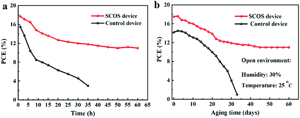 | ||
| Fig. 5 (a) UV-light stability of the control and SCOS PSCs under 365 nm UV-light irradiation. (b) Long-term stability of the control and SCOS PSCs in the ambient environment with a relative humidity of 30% and temperature of 25 °C. | ||
Conclusions
In summary, we have presented an effective approach to enhance the performance of PSCs by using a novel samarium-based down conversion material (SCOS), which can efficiently convert a broad UV spectrum to visible light, leading to increased light harvesting, reduced UV-light degradation and improved long-term stability of the PSCs. The Jsc, Voc, and FF of the SCOS devices are 23.65 mA cm−2, 1.05 V and 72.4, respectively, resulting in a high PCE of 17.9%, which is greater than the 15.4% for the control devices without the SCOS layer. When exposed to UV-light irradiation or an open environment under moisture conditions, the SCOS devices can maintain high photovoltaic performance for a much longer period than the control devices. These results suggest that incorporating UV down converting materials provides a promising strategy to construct PSCs with high performance and UV-light stability for future practical applications.Conflicts of interest
There are no conflicts to declare.Acknowledgements
This work was financially supported by the NSFC (51733010, 61605253, 21672267 and 51773230), the Science and Technology Planning Project of Guangdong (2015B090913003) and the Fundamental Research Funds for the Central Universities.References
- H. Zhou, Q. Chen, G. Li, S. Luo, T.-b. Song, H.-S. Duan, Z. Hong, J. You, Y. Liu and Y. Yang, Science, 2014, 345, 542 CrossRef CAS.
- M. Liu, M. B. Johnston and H. J. Snaith, Nature, 2013, 501, 395 CrossRef CAS.
- J. Burschka, N. Pellet, S.-J. Moon, R. Humphry-Baker, P. Gao, M. K. Nazeeruddin and M. Grätzel, Nature, 2013, 499, 316 CrossRef CAS.
- Q. Wang, Y. Shao, Q. Dong, Z. Xiao, Y. Yuan and J. Huang, Energy Environ. Sci., 2014, 7, 2359 RSC.
- S. Lv, L. Han, J. Xiao, L. Zhu, J. Shi, H. Wei, Y. Xu, J. Dong, X. Xu and D. Li, Chem. Commun., 2014, 50, 6931 RSC.
- D. Luo, W. Yang, Z. Wang, A. Sadhanala, Q. Hu, R. Su, R. Shivanna, G. F. Trindade, J. F. Watts, Z. Xu, T. Liu, K. Chen, F. Ye, P. Wu, L. Zhao, J. Wu, Y. Tu, Y. Zhang, X. Yang, W. Zhang, R. H. Friend, Q. Gong, H. J. Snaith and R. Zhu, Science, 2018, 360, 1442 CrossRef CAS.
- G. Xing, N. Mathews, S. Sun, S. S. Lim, Y. M. Lam, M. Grätzel, S. Mhaisalkar and T. C. Sum, Science, 2013, 342, 344 CrossRef CAS.
- Q. Dong, Y. Fang, Y. Shao, P. Mulligan, J. Qiu, L. Cao and J. Huang, Science, 2015, 347, 967 CrossRef CAS PubMed.
- C. C. Stoumpos, C. D. Malliakas and M. G. Kanatzidis, Inorg. Chem., 2013, 52, 9019 CrossRef CAS PubMed.
- M. A. Green, A. Ho-Baillie and H. J. Snaith, Nat. Photonics, 2014, 8, 506 CrossRef CAS.
- S. D. Stranks, G. E. Eperon, G. Grancini, C. Menelaou, M. J. Alcocer, T. Leijtens, L. M. Herz, A. Petrozza and H. J. Snaith, Science, 2013, 342, 341 CrossRef CAS PubMed.
- A. Kojima, K. Teshima, Y. Shirai and T. Miyasaka, J. Am. Chem. Soc., 2009, 131, 6050 CrossRef CAS PubMed.
- Best Research-Cell Efficiencies Chart, National Renewable Energy Laboratory (NREL), https://www.nrel.gov/pv/assets/pdfs/pv-efficiencies-07-17-2018.pdf.
- F. Li, Y. Zhang, K.-J. Jiang, C. Zhang, J.-H. Huang, H. Wang, H. Fan, P. Wang, Y. Chen, W. Zhao, X. Li, L.-M. Yang, Y. Song and Y. Li, Adv. Mater., 2018, 30, 1804454 CrossRef PubMed.
- Y. Wang, Y. Yue, X. Yang and L. Han, Adv. Energy Mater., 2018, 8, 1800249 CrossRef.
- M. Green, K. Emery, Y. Hishikawa, W. Warta and E. D. Dunlop, Prog. Photovolt: Res. Appl., 2015, 23, 805 CrossRef.
- M. Saliba, T. Matsui, J.-Y. Seo, K. Domanski, J.-P. Correa-Baena, M. K. Nazeeruddin, S. M. Zakeeruddin, W. Tress, A. Abate and A. Hagfeldt, Energy Environ. Sci., 2016, 9, 1989 RSC.
- F. Wang, W. Geng, Y. Zhou, H. H. Fang, C. J. Tong, M. A. Loi, L. M. Liu and N. Zhao, Adv. Mater., 2016, 28, 9986 CrossRef CAS PubMed.
- J. You, L. Meng, T.-B. Song, T.-F. Guo, Y. M. Yang, W.-H. Chang, Z. Hong, H. Chen, H. Zhou and Q. Chen, Nat. Nanotechnol., 2016, 11, 75 CrossRef CAS PubMed.
- F. Bella, G. Griffini, J. P. Correa-Baena, G. Saracco, M. Grätzel, A. Hagfeldt, S. Turri and C. Gerbaldi, Science, 2016, 354, 203 CrossRef CAS PubMed.
- L. Jiang, W. Chen, J. Zheng, L. Zhu, L. Mo, Z. Li, L. Hu, T. Hayat, A. Alsaedi, C. Zhang and S. Dai, ACS Appl. Mater. Interfaces, 2017, 9, 26958 CrossRef CAS PubMed.
- D. Bryant, N. Aristidou, S. Pont, I. Sanchez-Molina, T. Chotchunangatchaval, S. Wheeler, J. R. Durrant and S. A. Haque, Energy Environ. Sci., 2016, 9, 1655 RSC.
- H. J. Jung, D. Kim, S. Kim, J. Park, V. P. Dravid and B. Shin, Adv. Mater., 2018, 30, 1802769 CrossRef PubMed.
- T. Leijtens, G. E. Eperon, S. Pathak, A. Abate, M. M. Lee and H. J. Snaith, Nat. Commun., 2013, 4, 2885 CrossRef PubMed.
- N. Aristidou, I. Sanchez-Molina, T. Chotchuangchutchaval, M. Brown, L. Martinez, T. Rath and S. A. Haque, Angew. Chem., Int. Ed., 2015, 54, 8208 CrossRef CAS PubMed.
- S. Ito, S. Tanaka, K. Manabe and H. Nishino, J. Phys. Chem. C, 2014, 118, 16995 CrossRef CAS.
- J. T.-W. Wang, J. M. Ball, E. M. Barea, A. Abate, J. A. Alexander-Webber, J. Huang, M. Saliba, I. Mora-Sero, J. Bisquert and H. J. Snaith, Nano Lett., 2013, 14, 724 CrossRef PubMed.
- L. Qin, Z. Xie, L. Yao, Y. Yan, S. Pang, F. Wei and G. G. Qin, Phys. Status Solidi RRL, 2014, 8, 912 CrossRef CAS.
- A. Kojima, K. Teshima, Y. Shirai and T. Miyasaka, J. Am. Chem. Soc., 2009, 131, 6050 CrossRef CAS PubMed.
- H. S. Kim, C. R. Lee, J. H. Im, K. B. Lee, T. Moehl, A. Marchioro, S. J. Moon, R. Humphry-Baker, J. H. Yum, J. E. Moser, M. Gratzel and N. G. Park, Sci. Rep., 2012, 2, 591 CrossRef PubMed.
- M. M. Lee, J. Teuscher, T. Miyasaka, T. N. Murakami and H. J. Snaith, Science, 2012, 338, 643 CrossRef CAS PubMed.
- S. Yamaguchi and K. Tamao, J. Chem. Soc., Dalton Trans., 1998, 22, 3693 RSC.
- G. Lu, H. Usta, C. Risko, L. Wang, A. Facchetti, M. A. Ratner and T. J. Marks, J. Am. Chem. Soc., 2008, 130, 7670 CrossRef CAS PubMed.
- J. Hou, H.-Y. Chen, S. Zhang, G. Li and Y. Yang, J. Am. Chem. Soc., 2008, 130, 16144 CrossRef CAS PubMed.
- K. Gao, B. Xu, C. Hong, X. Shi, H. Liu, X. Li, L. Xie and A. K.-Y. Jen, Adv. Energy Mater., 2018, 8, 1800809 CrossRef.
- T. Leijtens, G. E. Eperon, S. Pathak, A. Abate, M. M. Lee and H. J. Snaith, Nat. Commun., 2013, 4, 2885 CrossRef PubMed.
- J. Jin, C. Chen, H. Li, Y. Cheng, L. Xu, B. Dong, H. Song and Q. Dai, ACS Appl. Mater. Interfaces, 2017, 9, 14518 CrossRef CAS PubMed.
- C. Chen, H. Li, J. Jin, Y. Cheng, D. Liu, H. Song and Q. Dai, Nano Energy, 2017, 32, 165 CrossRef CAS.
- N.-G. Park, Mater. Today, 2015, 18, 65 CrossRef CAS.
- P. Strange, A. Svane, W. Temmerman, Z. Szotek and H. Winter, Nature, 1999, 399, 756 CrossRef CAS.
- F. Auzel, Chem. Rev., 2004, 104, 139 CrossRef CAS PubMed.
- G. Wu, L. Zhang, B. Cheng, T. Xie and X. Yuan, J. Am. Chem. Soc., 2004, 126, 5976 CrossRef CAS PubMed.
- P. Hlawenka, K. Siemensmeyer, E. Weschke, A. Varykhalov, J. Sánchez-Barriga, N. Y. Shitsevalova, A. V. Dukhnenko, V. B. Filipov, S. Gabáni, K. Flachbart, O. Rader and E. D. L. Rienks, Nat. Commun., 2018, 9, 517 CrossRef CAS PubMed.
- T. Trupke, M. Green and P. Würfel, J. Appl. Phys., 2002, 92, 1668 CrossRef CAS.
- J. Liu, Q. Yao and Y. Li, Appl. Phys. Lett., 2006, 88, 173119 CrossRef.
- E. Klampaftis, D. Ross, K. R. McIntosh and B. S. Richards, Sol. Energy Mater. Sol. Cells, 2009, 93, 1182 CrossRef CAS.
- J. Shen, Z. Li, R. Cheng, Q. Luo, Y. Luo, Y. Chen, X. Chen, Z. Sun and S. Huang, ACS Appl. Mater. Interfaces, 2014, 6, 17454 CrossRef CAS PubMed.
- H. Hafez, M. Saif and M. Abdel-Mottaleb, J. Power Sources, 2011, 196, 5792 CrossRef CAS.
- N. Chander, A. Khan, P. Chandrasekhar, E. Thouti, S. K. Swami, V. Dutta and V. K. Komarala, Appl. Phys. Lett., 2014, 105, 033904 CrossRef.
- J. Roh, H. Yu and J. Jang, ACS Appl. Mater. Interfaces, 2016, 8, 19847 CrossRef CAS PubMed.
- W. Chen, Q. Luo, C. Zhang, J. Shi, X. Deng, L. Yue, Z. Wang, X. Chen and S. Huang, J. Mater. Sci.: Mater. Electron., 2017, 28, 11346 CrossRef CAS.
- X. Hou, T. Xuan, H. Sun, X. Chen, H. Li and L. Pan, Sol. Energy Mater. Sol. Cells, 2016, 149, 121 CrossRef CAS.
- C. W. Kim, T. Y. Eom, I. S. Yang, B. S. Kim, W. I. Lee, Y. S. Kang and Y. S. Kang, Sci. Rep., 2017, 7, 6849 CrossRef PubMed.
- C. Chen, H. Li, J. Jin, X. Chen, Y. Cheng, Y. Zheng, D. Liu, L. Xu, H. Song and Q. Dai, Adv. Energy Mater., 2017, 7, 1700758 CrossRef.
- P. Z. Zambare and O. H. Mahajan, Res. Rev.: J. Pure Appl. Phys., 2013, 1, 8 Search PubMed.
- L. An, J. Zhang, M. Liu, S. Chen and S. Wang, Opt. Mater., 2008, 30, 957 CrossRef CAS.
- A. Setlur, D. Porob, U. Happek and M. Brik, J. Lumin., 2013, 133, 66 CrossRef CAS.
- C. Zhang, S. Jianshe, Y. Xujie, L. Lude and W. Xin, J. Rare Earths, 2010, 28, 513 CrossRef CAS.
- K. Li, H. Xu, Z. Xu, M. Zeller and A. D. Hunter, Inorg. Chem., 2005, 44, 8855 CrossRef CAS PubMed.
- A. G. Bispo Jr, D. A. Ceccato, S. A. M. Lima and A. M. Pires, RSC Adv., 2017, 7, 53752 RSC.
- Q. Li, Y. Yuan, T. Wei, Y. Li, Z. Chen, X. Jin, Y. Qin and W. Sun, Sol. Energy Mater. Sol. Cells, 2014, 130, 426 CrossRef CAS.
- Y. Shao, Y. Fang, T. Li, Q. Wang, Q. Dong, Y. Deng, Y. Yuan, H. Wei, M. Wang and A. Gruverman, Energy Environ. Sci., 2016, 9, 1752 RSC.
- J. H. Heo, D. H. Song, H. J. Han, S. Y. Kim, J. H. Kim, D. Kim, H. W. Shin, T. K. Ahn, C. Wolf and T. W. Lee, Adv. Mater., 2015, 27, 3424 CrossRef CAS.
- X. Meng, J. Zhou, J. Hou, X. Tao, S. H. Cheung, S. K. So and S. Yang, Adv. Mater., 2018, 30, 1706975 CrossRef PubMed.
- X. Huang, S. Han, W. Huang and X. Liu, Chem. Soc. Rev., 2013, 42, 173 RSC.
- W. Chen, L. Xu, X. Feng, J. Jie and Z. He, Adv. Mater., 2017, 29, 1603923 CrossRef PubMed.
- Y. Shi, Y. Xing, Y. Li, Q. Dong, K. Wang, Y. Du, X. Bai, S. Wang, Z. Chen and T. Ma, J. Phys. Chem. C, 2015, 119, 15868 CrossRef CAS.
- K. Mahmood, B. S. Swain, A. R. Kirmani and A. Amassian, J. Mater. Chem. A, 2015, 3, 9051 RSC.
- S. Prathapani, V. More, S. Bohm, P. Bhargava, A. Yella and S. Mallick, Applied Materials Today, 2017, 7, 112 CrossRef.
- J. Zhang, Z. Hu, L. Huang, G. Yue, J. Liu, X. Lu, Z. Hu, M. Shang, L. Han and Y. Zhu, Chem. Commun., 2015, 51, 7047 RSC.
- N. Tripathi, Y. Shirai, M. Yanagida, A. Karen and K. Miyano, ACS Appl. Mater. Interfaces, 2016, 8, 4644 CrossRef CAS PubMed.
- C. He, C. Zhong, H. Wu, R. Yang, W. Yang, F. Huang, G. C. Bazan and Y. Cao, J. Mater. Chem., 2010, 20, 2617 RSC.
- Y. Kim, S. Cook, S. M. Tuladhar, S. A. Choulis, J. Nelson, J. R. Durrant, D. D. Bradley, M. Giles, I. McCulloch and C.-S. Ha, Nat. Mater., 2006, 5, 197 CrossRef CAS.
- A. Agresti, S. Pescetelli, L. Cinà, D. Konios, G. Kakavelakis, E. Kymakis and A. D. Carlo, Adv. Funct. Mater., 2016, 26, 2686 CrossRef CAS.
Footnote |
| † Electronic supplementary information (ESI) available. See DOI: 10.1039/c8ta09362h |
| This journal is © The Royal Society of Chemistry 2019 |