
 Open Access Article
 This Open Access Article is licensed under a
 Creative Commons Attribution 3.0 Unported Licence
Resistance-based analysis of limiting interfaces in multilayer water splitting photocathodes by impedance spectroscopy†
Thomas
Moehl
 ,
Wei
Cui
,
René
Wick-Joliat
and
S. David
Tilley
*
,
Wei
Cui
,
René
Wick-Joliat
and
S. David
Tilley
*
Department of Chemistry, University of Zurich, Winterthurerstrasse 190, CH-8057 Zurich, Switzerland. E-mail: david.tilley@chem.uzh.ch
First published on 17th June 2019
Abstract
Photoabsorber materials such as Cu2O, which are normally prone to degradation reactions in aqueous environment, have regained attention for photoelectrochemical water splitting (PEC) due to the use of protective overlayers. Furthermore, by implementing an additional interlayer between the photoabsorber and protective layer, the photovoltage and the overall device efficiency can be enhanced due to the increased built-in voltage at the p–n junction. The detailed analysis of these multilayer PEC photoelectrodes under operando conditions is challenging due to the multiplicity of interfaces and charge carrier processes. To facilitate routine investigation of such multilayer systems, we have established a resistance-based method using electrochemical impedance spectroscopy (EIS) to identify the underlying potential-dependent processes of water splitting photocathodes under operation, which quickly reveals the problematic interfaces in these structures. Cu2O/Ga2O3/TiO2/RuOx and p–Si/TiO2/RuOx photocathodes were investigated, with varying thicknesses of both interlayer and protection layer. The main limitations in the Cu2O devices were found to be the Ga2O3/TiO2 interface and the surface properties of the cuprous oxide absorber (most likely Cu2+ at the surface). We demonstrate that a commonly applied etching procedure of the Cu2O to remove surface impurities reduced the associated resistance, but was not sufficient to achieve an ideal interface to the electron accepting layer. The analysis scheme enabled us to shed light on most of the involved charge carrier processes taking place in these complex systems, and we expect that this method will be applicable to other multilayer systems, facilitating a more routine and powerful operando characterization method for water splitting photoelectrodes. Furthermore the knowledge gained in this investigation will pave the way for the development of a complete equivalent circuit model of these protected buried heterojunction photocathodes.
Introduction
Several promising photocathode absorber materials for PEC applications—normally prone to (photo)corrosion in aqueous electrolyte solution—can be stabilized by using protective overlayers such as TiO2, generating “buried junctions” where the photovoltage is generated at a solid-state junction underneath the semiconductor-electrolyte junction. Amongst these promising semiconductors are Cu2O,1,2 CuO,3 Si,4–7 III–V semiconductors,8,9 Cu2BaSnS4,10 Cu2ZnSnS4,11 and BiVO4.12,13 Additionally, semiconducting buffer layers such as Ga2O3 (ref. 2 and 14) or CdS3 can be inserted between the photoabsorber and protection layers to increase the built-in voltage, the charge separation and the overall device efficiency. A scheme of these multi-layer structures is presented in Fig. 1.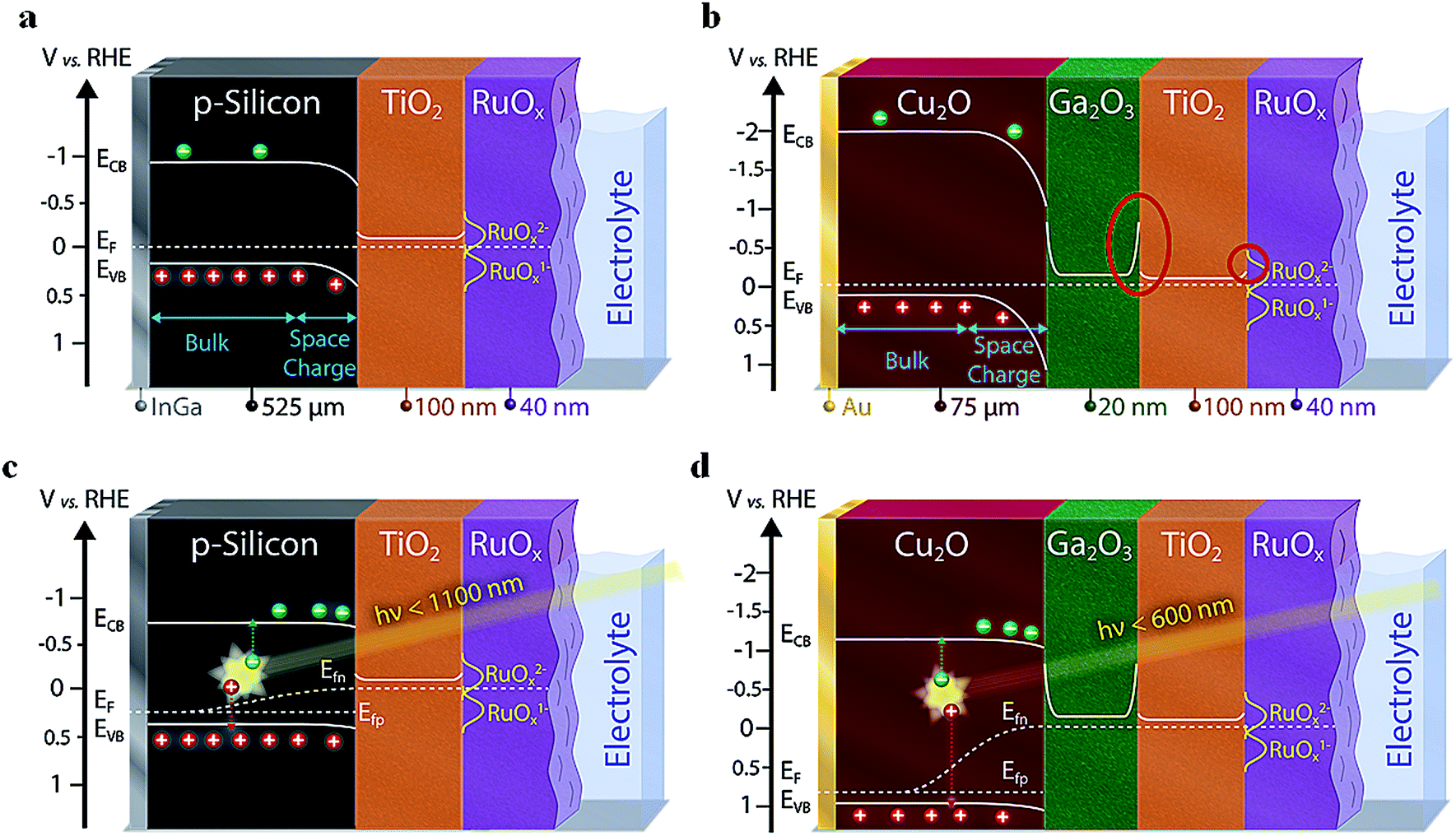 | ||
| Fig. 1 Band energy diagrams at equilibrium in the dark for (a) p-type silicon-based and (b) Cu2O-based devices (the red circles show potential barriers for the photogenerated electrons); (c) a Si- and (d) a Cu2O-based photocathode under illumination. | ||
Due to the high complexity of these photoelectrodes along with the involved charge carrier processes, in-depth routine analysis is challenging. So far, there are few reports on the systematic study on interface and charge transport limitations through the multilayered structure under operational conditions. A scheme of the most common photophysical and electrochemical processes taking place in PEC devices are depicted in Fig. S1.† Electrochemical impedance spectroscopy (EIS) is a powerful non-destructive characterization method widely applied in different fields such as solar cells15–18 and PEC systems.19–21 Devices can be investigated under operando conditions both in the dark and under illumination. In the dark, measurements are normally performed to facilitate a Mott–Schottky analysis, which gives access to the band alignment of the semiconductors as well as the doping density and type of the majority carriers (electrons or holes).22–24 In contrast, under illumination, the light induced processes, which are normally dominated by the minority charge carriers, can be evaluated and their implications for the device efficiency understood.
In PEC research, EIS under illumination has been applied to a variety of photoelectrodes, though interpretation of the data is not trivial, since an equivalent circuit (EC) model is required that sufficiently mimics the underlying photophysical and electrochemical processes in the system under study.19,21 Even for such a relatively simple and well investigated system as Fe2O3, several EC models have been developed, as surface treatments, nanostructuring and/or fabrication process conditions alter the properties of the material.20,25–28 Furthermore, the EI spectra can be complicated to analyze if two or more processes take place in the same time domain, as they can usually not be separated during the fitting procedure. On the other hand, the overall resistance of the two processes can be determined, which enables one to draw conclusions on their nature, especially if their potential dependence is investigated. Normally the capacitive elements distinguish the EC models, as the detected resistances are normally all in series (see Fig. S2†). Here, we apply a resistance-based analysis using EIS as a facile and generally applicable method to quickly identify the problematic layers and/or interfaces in these complex device architectures.
We investigated two systems, a more traditional photoabsorber material with relatively simple architecture (p-Si/TiO2/RuOx) as a well-behaved standard, and one based on the emerging material cuprous oxide (Cu2O/Ga2O3/TiO2/RuOx), which features a buffer layer and therefore contains additional interfaces. The heterojunction with Ga2O3 is of particular interest due to the high photovoltage that can be obtained (1.2 V).29
The n-type layer in the investigated photocathodes that is in contact with the electrolyte solution serves as both a protective layer and as an electron accepting layer. Commonly, TiO2 is used due to its good (photo)electrochemical stability over a wide range of pH. On the other hand, the built-in voltage between Si or Cu2O with TiO2 is relatively low. By implementing ZnO or AZO,30 ZnS,31 or Ga2O3 (ref. 14) as an interlayer, the built-in voltage and therefore also the photovoltage can be greatly increased for the Cu2O-based devices.29 The increased photovoltage is reflected in an earlier onset potential in J–V curves. The shift in onset potential of the photocurrent by the Ga2O3 interlayer is between 500 to 600 mV as compared to the devices with a direct Cu2O/TiO2 contact, reflecting the increased built-in voltage in the semiconductor heterojunction.
Results and discussion
Photocathodes in the dark
We first performed a Mott–Schottky analysis of the two photocathode types and of the ALD Ga2O3 to understand the energetic alignment of the different materials. The results on the built-in voltage (combined with the optical bandgap and the calculated distance of the EF to the valence and conduction band) are presented in Fig. 1. A more detailed description of the Mott–Schottky plots and the processing of the resulting data can be found in the ESI (Fig. S3, S4 and Table S2†). The position of the reduced redox states of the RuOx hydrogen evolving catalyst (namely Ru(III)Ox1− and Ru(II)Ox2−) have been implemented based on literature values and our own measurements (see Fig. S5† and main text below).32–34By evaluating the band diagrams in Fig. 1, potential barriers for photogenerated charge carriers are revealed. Such unfavorable band bending can lead to a limited charge transfer for electrons at the junction if the space charge forming the barrier is not thin enough (preventing tunneling). Indeed, we can conclude on the basis of Fig. 1a (for silicon) and Fig. 1b (for Cu2O) that there is one limiting junction for the charge transfer of electrons from the TiO2 to the catalyst, and in case of the Cu2O-based devices a second one between the Ga2O3 and the TiO2 (see red circles in Fig. 1b). Especially this latter one between the two n-type ALD layers could cause resistive limitations for the electron flow. We emphasize at this point that Mott–Schottky plot analysis must be taken as a first approximation of the actual band alignments in the PEC photocathodes. For example, the conduction band edges of the Ga2O3 with the photoabsorber and the TiO2 will most probably not be symmetrical, but will still show the two potential barriers between Cu2O/Ga2O3 and Ga2O3/TiO2 as indicated in Fig. 1b.
Photocathodes under illumination
Typical J–V curves of the two systems are presented in Fig. 2. The photocurrent onset is shifted ∼0.6 V for the Cu2O-based device, showing the higher built-in voltage as compared to the silicon devices. On the other hand, the J–V curve of the Cu2O-based devices is more resistive, showing a lower fill factor (FF). When plotting the photocurrent logarithmically, three distinct regions are observed, which are also found in the resistances extracted from the EIS spectra (Fig. 3). In region I, at most positive potentials, a small (photo)anodic current is observed (nA to μA cm−2). This phenomenon can also be observed for other photocathodes35–38 and originates from the leakage current of the majority carriers. In region II, the electron quasi Fermi level is negative enough (on the RHE scale) so that the catalyst is reduced from RuOx to RuOx−1 by injecting electrons into the Gaussian shaped density of states (DOS) of the catalyst, showing photocathodic current (μA cm−2).32 Still most of the photogenerated charge carriers are subject to recombination as the electrochemical potential of the H2 evolution has not yet been reached. In region III, the hydrogen evolution current can be observed as the electron quasi Fermi level has reached the second reduction step of the catalyst and the hydrogen evolution potential. The protons present in the electrolyte solution then act as electron acceptor, now enabling the charge transfer and the photocurrent generation.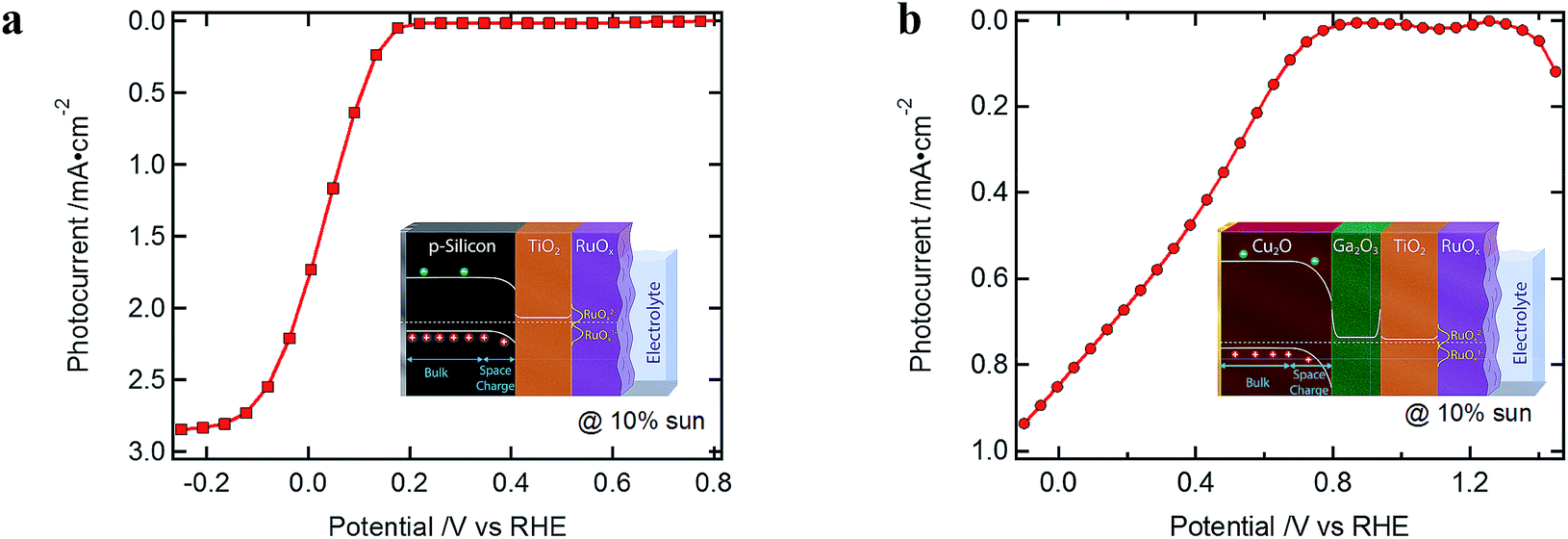 | ||
| Fig. 2 Typical J–V curves (a) of a silicon-(100 nm ALD TiO2 and RuOx) and (b) of a Cu2O-(20 nm ALD Ga2O3, 100 nm ALD TiO2 and RuOx) based standard device, under white light illumination of 10% sun. | ||
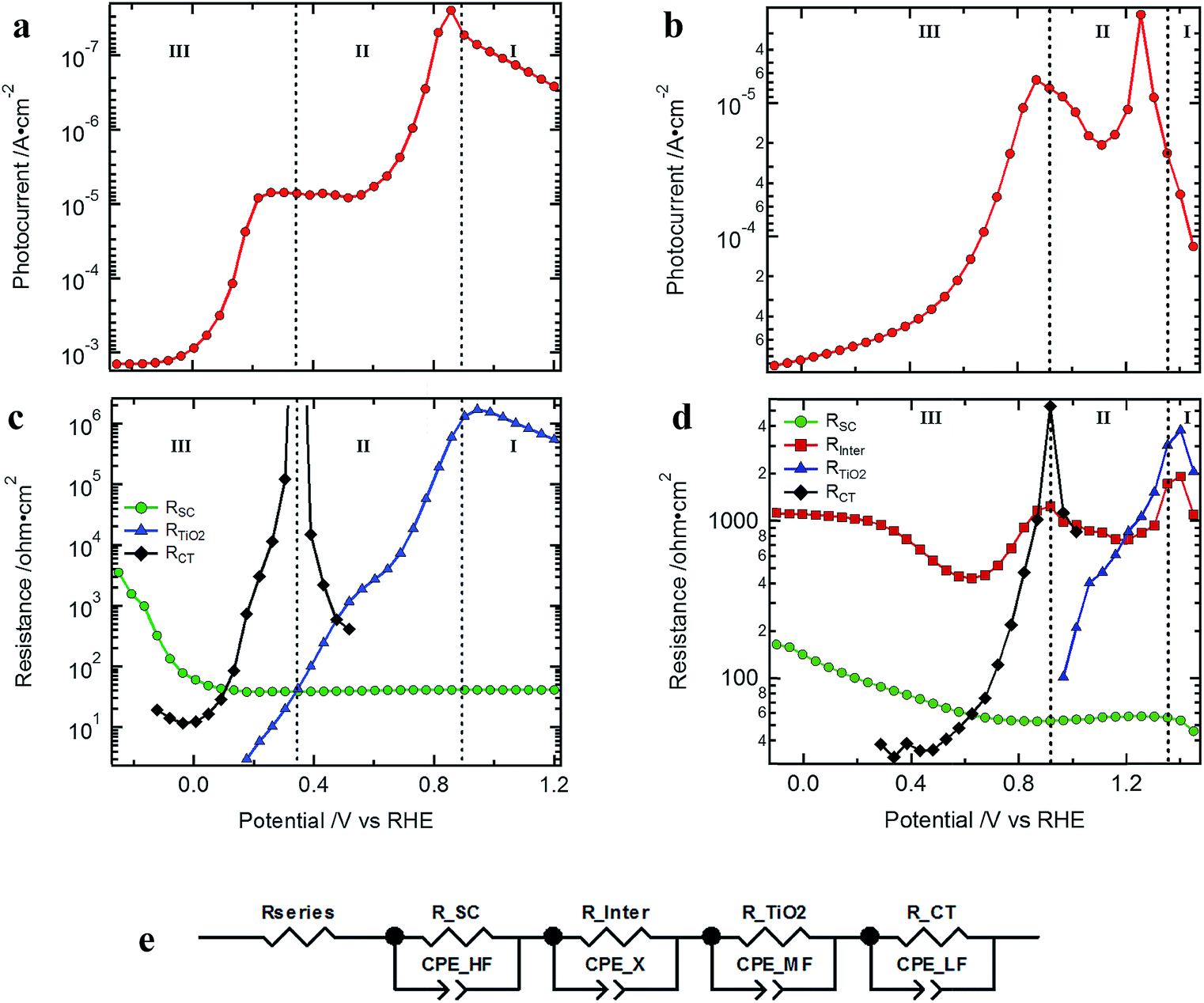 | ||
| Fig. 3 Logarithm of the photocurrent of the devices presented in Fig. 2: (a) Si- and (b) Cu2O-based standard devices (light intensity of 10%); resistances from the EIS fitting procedure of the (c) Si- and (d) Cu2O-based standard devices; (e) EC model used to fit the EIS data (for the silicon devices the RC element of Rinter is omitted as it was not present). | ||
Comparing the different resistances determined for the Si and Cu2O devices by EIS analysis (see Nyquist and Bode plots in Fig. S6 and S7† as well as Table S1† for associated frequencies), we can also observe three distinct potential regions, which coincide with those of the photocurrent plots (Fig. 3c and d). Furthermore, clear similarities in the potential dependent behavior of the resistances can be noted between the different photocathode types. The low frequency resistance RCT (charge transfer resistance) has a strong potential dependence for both photocathode types. Also, RTiO2 and RSC (related to the TiO2 layer and the recombination resistance inside the semiconductor junction, respectively) show clear changes with applied potential. Rinter (discussed in detail below), in contrast, is only present in the Cu2O-based devices and is rather constant with potential, though showing a valley at ∼0.6 V vs. RHE and another one at ∼1.2 V vs. RHE.
The similarities between the resistances of the different photocathodes are even more evident when accounting for the different photovoltages in each system: after shifting the data to give the same quasi-Fermi level of electrons (set by the onset of the hydrogen evolution current as determined by RCT at the beginning of region III), the J–V curves and extracted resistances of the Si and Cu2O devices overlap with one another, enabling a direct comparison (Fig. S8†). The detection of the onset potential via RCT is more sensitive as compared to the extrapolation of the photocurrent to the voltage axis or by setting an arbitrary (low) photocurrent as a measure.
The low frequency resistance, RCT, mirrors the shape of the J–V curves in potential region III (Fig. 3c and d) and represents the hydrogen-generating charge transfer over the hydrogen evolving catalyst (HEC) into the electrolyte solution (RCT–H2 in Fig. 4). Prior to the onset of hydrogen evolution in potential region II, RTiO2 shows a deviation from exponential behavior representing the increased current flow for the HEC reduction (Fig. S9†). In part of this potential region, RCT is convoluted with RTiO2. For the Si-based devices, the separation of RCT and RTiO2 could be achieved by extrapolating an exponential decrease of RTiO2 and subtracting it in the potential region of the first HEC reduction (RCT–RuOx in Fig. 4). In the case of the Cu2O devices, the separation did not yield reliable results due to the interference with the additional resistance Rinter.
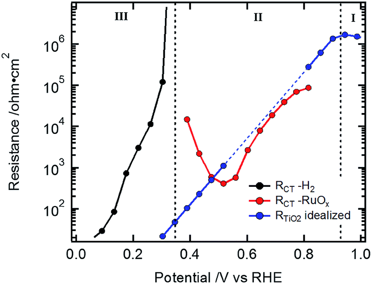 | ||
| Fig. 4 Data from Si sample in Fig. 2a: exponential extrapolation of RTiO2 (blue dotted line) and the residual resistance (RCT–RuOx) relating to the current for the HEC reduction. | ||
R CT–RuOx itself mirrors the current flow for the first reduction step of RuOx to form RuOx−1 (from Ru(IV) to Ru(III)), which is a prerequisite for hydrogen evolution.32–34,39,40 Notably, the shape of RCT–RuOx reflects the DOS of the catalyst. RuOx as the HEC can be seen as a protonic electrochemical capacitor due to H+ exchange with the electrolyte solution: RuOx(OH)y + δH+ + δe− ↔ RuOx−δ(OH)y+δ (see also ESI and Fig. S5† for further discussion on the redox states of the HEC).39,40 The charge inside the HEC can be visualized by its storage and release process during transient photocurrent decay measurements (TPC).32,41 In the TPC experiments, a steady state white light bias was applied (10% sun). The wavelengths of the light pulse to generate the photocurrent transients was either 447 nm (Fig. 5a) or 530 nm (Fig. 5b), which led to an excitation of charge carriers near the surface of the photoabsorber. The possible excitation at 627 nm (red) is near the absorption onset of the Cu2O and would therefore probe the bulk of the semiconductor with the deeper penetration depth of this wavelength (see Niu et al.).2 As the focus in the TPC experiments was the detection of the charge inside the HEC, we have used a perturbation pulse with 5 to 10% of a sun as light intensity (i.e. 50 to 100% of the actual white light bias). Therefore, our TPC measurements are not “small” perturbation experiments near equilibrium but rather photocurrent transients similar to the investigations by Laskowski et al. with a strong perturbation.41 The TPC measurements were performed similar to the EIS measurements at different bias potentials to further observe the potential dependent changes of the accumulated charge.
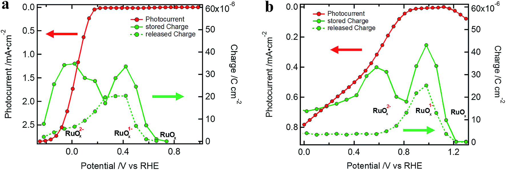 | ||
| Fig. 5 Stored and released charge in the TPC (measurements with 10% sun white light bias) showing the charging of the RuOx catalyst for (a) a Si device (excitation at 447 nm (5% sun), same sample as in Fig. 2a) and (b) a Cu2O standard device (excitation at 530 nm (10% sun)), Cu2O standard device) device. | ||
During the light pulse, normally a double-exponential decay of the photocurrent was observed. The fast component of the decay is associated with the recombination of photogenerated charge carriers while the slow one is related to the formation of RuOx1− or RuOx2− species.32 After the light pulse is turned off, the photocurrent steeply drops and changes sign before returning to the steady state white light bias current. The photocurrent with inverted sign represents the release of stored charge inside the HEC (the decay back to steady state white light bias current was normally mono-exponential). Examples of the TPC transients can be found in Fig. S10† together with a table of the exponential fittings (Tables S3 and S4†).
The charge in a current transient was determined from the integral of the exponential decay of the current density over pulse duration (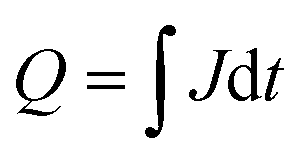 ; with Q as the charge per cm2, J as the current density and t as time). The amount of charge determined in the TPC experiments for the storage (from the slow component of the photocurrent decay during the light pulse) and release (after the light pulse has been turned off) process are very similar and show the capacitive loading of the HEC at its different redox states (Fig. 5, see also Table S5†). As the release of stored charge is competing with the hydrogen evolution reaction, normally the amount of released charge detected is lower as compared to the initially stored charge, especially near the RuOx2− redox potential.
R TiO2 is a strongly potential dependent resistance at intermediate frequencies present in potential regions I and II (Fig. 3). At very positive potentials RTiO2 dominates the photoanodic current flow. In region II RTiO2 decreases exponentially but shows a deviation in the form of a valley as discussed above. After the formation of RuOx−1, RTiO2 further decreases exponentially. As both the Si and Cu2O-based systems possess the TiO2 protection layer and the associated interfaces (TiO2/catalyst or the TiO2/electrolyte solution), one possibility is that RTiO2 is related to a resistive transport inside the TiO2, or a second possibility is that it is related to a potential barrier at the aforementioned interfaces (for both of these cases, RTiO2 manifests as a series resistance). To differentiate these options, we varied the protection layer thickness between 50, 100 and 150 nm. A transport related resistance should show a significant increase for the thicker protection layers while a resistance related to a potential barrier at the TiO2/RuOx interface would not be influenced by the different thicknesses of the TiO2 layer. The results for Cu2O and silicon (Fig. S11†) did not show any significant change in the resistance with increasing thickness of the ALD TiO2 layer. A charge transport resistance within the TiO2 can therefore be excluded. Considering the observation in Fig. 1a and b of the unfavorable band bending at the TiO2 contact to the catalyst we can conclude that RTiO2 represents the resistive limitation at this interface. The implications, however, for the overall device efficiency of this series resistance are limited to the photocurrent rise, as it is low or vanished when the surface potential approaches the thermodynamic HER potential. An additional observation is that the thickness of the TiO2 layer did not have any significant influence on the VOC nor on the photocurrent.
The resistance at the highest frequencies, RSC, is mainly constant in the potential regions I and II and increases in region III. It is related to the recombination current of the photogenerated charge carriers and the steeper its increase in potential region III the better the FF of the J–V curves. The increase of RSC with increasing reverse bias after passing the H2 evolution potential represents the reduced recombination of photogenerated electron hole pairs (i.e. higher recombination resistance) as now the band bending in the space charge of the photoabsorber increases and acceptor states are available inside the electrolyte solution to enable the flow of photocurrent. It should be noted that in PEC photoelectrodes, the system is effectively in open-circuit until the surface potential is in a region where charge transfer can occur. Thus, if the quasi Fermi level of the electrons has not reached the second reduction step of the catalyst and the energetic position of the hydrogen evolution potential, the photogenerated charge must recombine (i.e. low recombination resistance, potential region I and II).42 The observation that RSC increases more slowly in the case of the Cu2O as compared to the Si samples (see Fig. 3 and S8†) originates from an additional series resistance that is present in the metal oxide-based devices, namely Rinter.
So far, the three different resistances described have been observed in both photocathode types. In the case of the fourth resistance, Rinter, observed only in the cuprous oxide devices, it stands to reason that it is related to the Ga2O3 layer or the Cu2O surface (or interface). Though Rinter shows as mentioned one valley around the second reduction of the catalyst, the valley at the first reduction step is not always clearly visible and is therefore disregarded in the analysis.
Generally, one would expect a reduction of Rinter similar to RTiO2 with increasing negative potential if it is purely related to a potential barrier at the Ga2O3/TiO2 interface. Compared to RTiO2 this reduction of the barrier would appear only after the electron quasi Fermi level reaches the redox potential of the H2 evolution potential, as only then the barrier at the Ga2O3/TiO2 interface would begin to reduce. This behavior is what we can observe in the descent into the valley starting from 0.8 V vs. RHE in Fig. 3d and 6 (for devices with Ga2O3 layer).
 | ||
| Fig. 6 (a) J–V curves of Cu2O devices without and with 20 and 70 nm ALD Ga2O3 (and with 100 nm ALD TiO2 and RuOx); (b) J–V curves adjusted to the hydrogen evolution onset as determined by RCT; (c) Rinter as determined from the EIS measurements and (d) Rinter adjusted by RCT. | ||
However, Rinter starts to increase again after passing 0.6 V vs. RHE, indicating that it is a superposition of different contributions. To better understand Rinter, Cu2O-based devices without the ALD Ga2O3 layer were fabricated and evaluated. In Fig. 6, the J–V curves and Rinter of devices without and with 20 and 70 nm ALD Ga2O3 layer are plotted before (a and c) and after (b and d) adjusting to the H2 evolution onset potential by RCT. As expected, the built-in voltage (see Fig. S3b†) and the photovoltage for devices without Ga2O3 layer are lower but interestingly Rinter is still present, albeit with a different potential dependence. It has a constant and low value in potential region I and II at positive potentials before the onset of the photocurrent (∼90 ohm cm2 as compared to ∼1000 ohm cm2 for the case with 20 nm Ga2O3 interlayer, Fig. 6), and then increases at more negative potentials.
This observation shows that the Cu2O surface properties are of crucial importance for high device efficiencies, as surface traps or an unwanted overlayer are limiting the charge transfer to the n-type semiconductor (discussed in more detail below). The magnitude of the Rinter (for devices with Ga2O3 layer) in potential region II correlates with the increased VOC observed in the devices. And in potential region III Rinter represents the series resistance that dominates the fill factor of the J–V curves (Fig. S12†), pinpointing the main limitation for the FF of the Cu2O photocathodes.
These observations on Rinter (series resistance in Region III, VOC correlation in region II, and existence even without the Ga2O3 interlayer (though in latter case with a different potential dependence)) imply that it is composed of at least two components (see Fig. S13†). One component, as visible for the case with 0 nm of Ga2O3, must be related to the Cu2O surface properties (Rsurface). The second contribution must be related to the ALD Ga2O3 interlayer (RGa) at the Ga2O3/TiO2 interface. The height of RGa in potential region II is accompanied with a higher built-in voltage and VOC (see also Mott–Schottky plots in Fig. S3b†). With 20 nm Ga2O3 still no bulk of the buffer layer can be formed as the layer is to thin and the full heterojunction potential is therefore lower as compared to 70 nm of buffer layer (in which the bulk can be already formed, see Fig. S14a–c†). Higher built-in voltage in turn increases the barrier height at the Ga2O3/TiO2 interface and the associated resistance.
To better understand the potential dependence of RGa we have to consider the interplay of the redox potential in solution, the applied potential and the position of the conduction bands of Ga2O3 and TiO2. Before the H2 onset potential, the barrier between Ga2O3 and TiO2 remains unchanged (Fig. S14d†). At the onset of the H2 evolution the potential barrier at the interface between the Ga2O3 and the TiO2 will start to decrease as the Fermi level inside the TiO2 layer is now pinned by the redox potential of the hydrogen evolution potential inside the electrolyte solution. On the other hand, the conduction band of Ga2O3 will continue to move to higher energies with scanning to more negative potentials (Fig. S14e and f†), reducing the barrier between the two n-type metal oxides. This will manifest as an exponential decrease of the RGa if it is related to a potential barrier (as for the case of RTiO2).
Indeed, RGa is, like RTiO2, reducing exponentially with increasing reverse bias, limiting its influence on the J–V curve mainly to the region of the hydrogen evolution current onset (see Fig. 6d). The relation between the built-in voltage and the change of RGa further supports our interpretation that it represents the potential barrier predicted by the Mott–Schottky plots (in Fig. 1d).
It is known that Cu2O in ambient conditions undergoes surface oxidation to Cu2+ species such as Cu(OH)2 or CuO, which can limit the performance of the devices.43 According to Lee et al.29 a reduction of the Cu2+ species by the gallium ALD precursor is possible as the authors have shown by XPS measurements which should improve the surface quality. Still we have implemented an additional etching of the Cu2O surface as a first cleaning process.43 Therefore, the as-prepared Cu2O sample was immersed in nitric acid (1![[thin space (1/6-em)]](https://www.rsc.org/images/entities/char_2009.gif) :1 of H2O and 65% HNO3) for 10 seconds, followed by rinsing with DI water and sonication in isopropanol for 30 seconds. Finally, the foil was dried under nitrogen flow and immediately transferred into the ALD chamber for the ALD buffer layer deposition.
:1 of H2O and 65% HNO3) for 10 seconds, followed by rinsing with DI water and sonication in isopropanol for 30 seconds. Finally, the foil was dried under nitrogen flow and immediately transferred into the ALD chamber for the ALD buffer layer deposition.
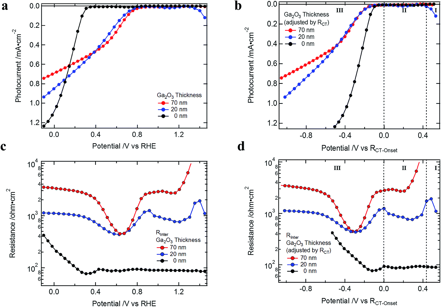
In Fig. 7, the results for devices with and without etching are presented. Devices were measured without the Ga2O3 layer to avoid superposition with the RGa component of Rinter. The performance of the pre-etched devices showed an increased FF due to the reduced Rsurface at the Cu2O/TiO2 contact (which could also be observed for the case with ALD Ga2O3 buffer layer, Fig. S15†). Nevertheless, Rsurface is still present after the etching, implying that the surface treatment is not sufficient to achieve a defect free interface. This resistance is probably induced by an energetically low-lying energy state at the surface through which the electrons must flow in order to cross over to the buffer layer. In contrast to RGa, the Cu2O surface resistance, Rsurface, would not reduce with further reverse bias. It increases as the conduction band of Ga2O3 shifts up at more negative applied potential, increasing the barrier for the electrons that have to be transferred through the limiting Cu2O surface layer (see Fig. S14d–f†).
 | ||
| Fig. 7 (a) J–V curves of Cu2O-based devices with and without etching treatment (devices are without ALD Ga2O3 but 100 nm ALD TiO2 and RuOx); (b) Rsurface of the samples presented in (a). | ||
Combining the knowledge about the potential dependence of Rinter with and without the Ga2O3 layer, we can conclude that Rinter is the source of the main limitations observed in the J–V curves. We can achieve high photovoltages, but the fill factor is limited by the resistive components of Rinter. Our results can explain now e.g. why Lee et al. observed for their Cu2O/Ga2O3-based solar cell devices high photovoltages of 1.2 V but a hampered FF of only 45%.29
The resistances observed in the EIS spectra under illumination have been assigned to the relevant charge carrier processes, and we can understand their influence on the J–V curves, a precondition to make sophisticated routine analysis and to facilitate the development of a generally applicable EC. Further investigations are being conducted to tackle the limitations observed in the Cu2O devices. On the one hand, we expect that the decrease of the space charge layer width through increased doping of the Ga2O3 layer would reduce the potential barrier and therefore the associated resistance for the electrons at the Ga2O3/TiO2 interface, and may enable both high VOC and FF. Furthermore, the higher doping would enable to achieve a higher built-in voltage at lower buffer layer thickness. On the other hand, with the presented analysis approach, we can evaluate the effect of different surface treatments on Rsurface and optimize the surface cleaning process, which should finally lead to a better FF and overall device efficiency.
Conclusion
We have investigated silicon- and Cu2O-based multilayer photocathode devices by EIS in the dark and under illumination to pinpoint the limitations for the J–V curves and device efficiencies. Based on the dark measurements we have identified potential barriers at the TiO2/RuOx and Ga2O3/TiO2 interfaces. Under illumination conditions we have analyzed the EIS data in terms of the potential dependence of the determined resistances. We have shown that shifting the data to align the hydrogen onset potential in the different samples (determined by the onset of the hydrogen evolution via the charge transfer resistance) enables the comparison of similar device types with different photovoltage and even different photocathode absorber materials. The resistances were assigned to the related photophysical or electrochemical processes, namely, the recombination of photogenerated charge carriers in the bulk or space charge region of the semiconductor, the charge transfer into the electrolyte solution, and the limited charge transfer due to a potential barrier between the TiO2 and the electrolyte solution. In the case of the Cu2O-based devices, an additional resistance appears, convoluting several different processes such as charge transfer from the absorber to the n-type semiconductor and a potential barrier at the Ga2O3/TiO2 interface. Based on our analysis we can conclude that this emerging photocathode material is hampered by its surface quality (i.e. interface defects), limiting the charge transfer between the Cu2O and the buffer layer and therefore the fill factor for these devices. The series resistance associated with the Cu2O surface could be reduced by a commonly applied etching treatment of the Cu2O surface, but our analysis shows directly that such a pre-treatment is not sufficient to achieve an ideal or nearly ideal surface that enables reproducibly high efficiency devices. We further identified a potential barrier for the photogenerated electrons at the Ga2O3/TiO2 interface which limits the rise of the photocurrent at the onset of the hydrogen evolution. By this analysis scheme we have opened the way for a fast and better understanding of the interplay of the different materials and interfaces and how to evaluate optimization treatments in complete multilayer device structures. Finally, the knowledge gained on the determined resistances and their associated photophysical and electrochemical processes will advance the development of a generally applicable EC of these multilayer photocathode systems.Conflicts of interest
The authors declare no competing financial interest.Acknowledgements
The University of Zurich Research Priority Program (URPP) LightChEC, and the Swiss National Science foundation (AP Energy Grant # PYAPP2 160586) are gratefully acknowledged for financial support.References
- L. Pan, J. H. Kim, M. T. Mayer, M.-K. Son, A. Ummadisingu, J. S. Lee, A. Hagfeldt, J. Luo and M. Grätzel, Nat. Catal., 2018, 1, 412 CrossRef CAS.
- W. Niu, T. Moehl, W. Cui, R. Wick-Joliat, L. Zhu and S. D. Tilley, Adv. Energy Mater., 2018, 8, 1702323 CrossRef.
- W. Septina, R. R. Prabhakar, R. Wick, T. Moehl and S. D. Tilley, Chem. Mater., 2017, 29, 1735 CrossRef CAS.
- D. Bae, T. Pedersen, B. Seger, M. Malizia, A. Kuznetsov, O. Hansen, I. Chorkendorff and P. C. K. Vesborg, Energy Environ. Sci., 2015, 8, 650 RSC.
- B. Seger, T. Pedersen, A. B. Laursen, P. C. K. Vesborg, O. Hansen and I. Chorkendorff, J. Am. Chem. Soc., 2013, 135, 1057 CrossRef CAS PubMed.
- A. G. Scheuermann, J. P. Lawrence, K. W. Kemp, T. Ito, A. Walsh, C. E. D. Chidsey, P. K. Hurley and P. C. McIntyre, Nat. Mater., 2016, 15, 99 CrossRef CAS PubMed.
- S. W. Boettcher, J. M. Spurgeon, M. C. Putnam, E. L. Warren, D. B. Turner-Evans, M. D. Kelzenberg, J. R. Maiolo, H. A. Atwater and N. S. Lewis, Science, 2010, 327, 185 CrossRef CAS PubMed.
- J. Gu, Y. Yan, J. L. Young, K. X. Steirer, N. R. Neale and J. A. Turner, Nat. Mater., 2016, 15, 456 CrossRef CAS PubMed.
- W.-H. Cheng, M. H. Richter, M. M. May, J. Ohlmann, D. Lackner, F. Dimroth, T. Hannappel, H. A. Atwater and H.-J. Lewerenz, ACS Energy Lett., 2018, 3, 1795 CrossRef CAS.
- J. Ge, P. J. Roland, P. Koirala, W. Meng, J. L. Young, R. Petersen, T. G. Deutsch, G. Teeter, R. J. Ellingson, R. W. Collins and Y. Yan, Chem. Mater., 2017, 29, 916 CrossRef CAS.
- K. Wang, D. Huang, Y. Le, H. Gu, S. Ikeda and F. Jiang, J. Colloid Interface Sci., 2019, 536, 9 CrossRef CAS PubMed.
- D. Lee, A. Kvit and K.-S. Choi, Chem. Mater., 2018, 30, 4704 CrossRef CAS.
- M. T. McDowell, M. F. Lichterman, J. M. Spurgeon, S. Hu, I. D. Sharp, B. S. Brunschwig and N. S. Lewis, J. Phys. Chem. C, 2014, 118, 19618 CrossRef CAS.
- C. Li, T. Hisatomi, O. Watanabe, M. Nakabayashi, N. Shibata, K. Domen and J.-J. Delaunay, Energy Environ. Sci., 2015, 8, 1493 RSC.
- I. Mora-Seró, Y. Luo, G. Garcia-Belmonte, J. Bisquert, D. Muñoz, C. Voz, J. Puigdollers and R. Alcubilla, Sol. Energy Mater. Sol. Cells, 2008, 92, 505 CrossRef.
- I. Mora-Seró, G. Garcia-Belmonte, P. P. Boix, M. A. Vázquez and J. Bisquert, Energy Environ. Sci., 2009, 2, 678 RSC.
- J.-H. Yum, E. Baranoff, F. Kessler, T. Moehl, S. Ahmad, T. Bessho, A. Marchioro, E. Ghadiri, J.-E. Moser, C. Yi, M. K. Nazeeruddin and M. Grätzel, Nat. Commun., 2012, 3, 631 CrossRef PubMed.
- R. Scheer and H. W. Schock, Chalcogenide photovoltaics. Physics, technologies, and thin film devices, Wiley-VCH, Weinheim, Germany, 2011 Search PubMed.
- L. Bertoluzzi and J. Bisquert, J. Phys. Chem. Lett., 2012, 3, 2517 CrossRef CAS PubMed.
- B. Klahr, S. Gimenez, F. Fabregat-Santiago, J. Bisquert and T. W. Hamann, J. Am. Chem. Soc., 2012, 134, 16693 CrossRef CAS PubMed.
- Photoelectrochemical solar fuel production. From basic principles to advanced devices, ed. S. Giménez and J. Bisquert, Springer International Publishing, Cham, 2016 Search PubMed.
- W. P. Gomes and D. Vanmaekelbergh, Electrochim. Acta, 1996, 41, 967 CrossRef CAS.
- R. de Gryse, W. P. Gomes, F. Cardon and J. Vennik, J. Electrochem. Soc., 1975, 122, 711 CrossRef CAS.
- O. Almora, C. Aranda, E. Mas-Marzá and G. Garcia-Belmonte, Appl. Phys. Lett., 2016, 109, 173903 CrossRef.
- T. Lopes, L. Andrade, H. A. Ribeiro and A. Mendes, Int. J. Hydrogen Energy, 2010, 35, 11601 CrossRef CAS.
- C. Y. Cummings, F. Marken, L. M. Peter, K. G. U. Wijayantha and A. A. Tahir, J. Am. Chem. Soc., 2012, 134, 1228 CrossRef CAS PubMed.
- V. Aroutiounian, Int. J. Hydrogen Energy, 2002, 27, 33 CrossRef CAS.
- F. Le Formal, S. R. Pendlebury, M. Cornuz, S. D. Tilley, M. Grätzel and J. R. Durrant, J. Am. Chem. Soc., 2014, 136, 2564 CrossRef CAS PubMed.
- Y. S. Lee, D. Chua, R. E. Brandt, S. C. Siah, J. V. Li, J. P. Mailoa, S. W. Lee, R. G. Gordon and T. Buonassisi, Adv. Mater., 2014, 26, 4704 CrossRef CAS PubMed.
- A. Paracchino, V. Laporte, K. Sivula, M. Grätzel and E. Thimsen, Nat. Mater., 2011, 10, 456 CrossRef CAS PubMed.
- P. Dai, W. Li, J. Xie, Y. He, J. Thorne, G. McMahon, J. Zhan and D. Wang, Angew. Chem., Int. Ed., 2014, 53, 13493 CrossRef CAS PubMed.
- E. Pastor, F. Le Formal, M. T. Mayer, S. D. Tilley, L. Francàs, C. A. Mesa, M. Grätzel and J. R. Durrant, Nat. Commun., 2017, 8, 14280 CrossRef CAS PubMed.
- K. Doblhofer, M. Metikoš, Z. Ogumi and H. Gerischer, J. Phys. Chem., 1978, 82, 1046 CAS.
- E. Watanabe, H. Ushiyama, K. Yamashita, Y. Morikawa, D. Asakura, M. Okubo and A. Yamada, J. Phys. Chem. C, 2017, 121, 18975 CrossRef CAS.
- M. J. Choi, J.-Y. Jung, M.-J. Park, J.-W. Song, J.-H. Lee and J. H. Bang, J. Mater. Chem. A, 2014, 2, 2928 RSC.
- J. Feng, M. Gong, M. J. Kenney, J. Z. Wu, B. Zhang, Y. Li and H. Dai, Nano Res., 2015, 8, 1577 CrossRef CAS.
- M. G. Mali, H. Yoon, B. N. Joshi, H. Park, S. S. Al-Deyab, D. C. Lim, S. Ahn, C. Nervi and S. S. Yoon, ACS Appl. Mater. Interfaces, 2015, 7, 21619 CrossRef CAS PubMed.
- L. Zhang, Y. Li, C. Li, Q. Chen, Z. Zhen, X. Jiang, M. Zhong, F. Zhang and H. Zhu, ACS Nano, 2017, 11, 12753 CrossRef CAS PubMed.
- S. Ardizzone, G. Fregonara and S. Trasatti, Electrochim. Acta, 1990, 35, 263 CrossRef CAS.
- J. Juodkazytė, R. Vilkauskaitė, B. Šebeka and K. Juodkazis, Trans. IMF, 2007, 85, 194 CrossRef.
- F. A. L. Laskowski, J. Qiu, M. R. Nellist, S. Z. Oener, A. M. Gordon and S. W. Boettcher, Sustainable Energy Fuels, 2018, 2, 1995 RSC.
- W. Cui, W. Niu, R. Wick-Joliat, T. Moehl and S. D. Tilley, Chem. Sci., 2018, 9, 6062 RSC.
- C. Xiang, G. M. Kimball, R. L. Grimm, B. S. Brunschwig, H. A. Atwater and N. S. Lewis, Energy Environ. Sci., 2011, 4, 1311 RSC.
Footnote |
| † Electronic supplementary information (ESI) available. See DOI: 10.1039/c9se00248k |
| This journal is © The Royal Society of Chemistry 2019 |