
 Open Access Article
 This Open Access Article is licensed under a
 Creative Commons Attribution 3.0 Unported Licence
Demonstration of a 50 cm2 BiVO4 tandem photoelectrochemical-photovoltaic water splitting device†
Ibbi Y.
Ahmet‡
 a,
Yimeng
Ma‡
a,
Ji-Wook
Jang
a,
Tobias
Henschel
b,
Bernd
Stannowski
b,
Tânia
Lopes
c,
António
Vilanova
c,
Adélio
Mendes
c,
Fatwa F.
Abdi
*a and
Roel
van de Krol
*a
a,
Yimeng
Ma‡
a,
Ji-Wook
Jang
a,
Tobias
Henschel
b,
Bernd
Stannowski
b,
Tânia
Lopes
c,
António
Vilanova
c,
Adélio
Mendes
c,
Fatwa F.
Abdi
*a and
Roel
van de Krol
*a
aInstitute for Solar Fuels, Helmholtz-Zentrum Berlin für Materialien und Energie GmbH, Hahn-Meitner-Platz 1, 14109 Berlin, Germany. E-mail: roel.vandekrol@helmholtz-berlin.de; fatwa.abdi@helmholtz-berlin.de
bPVcomB, Helmholtz-Zentrum Berlin für Materialien und Energie GmbH, Schwarzschildstr. 3, 12489 Berlin, Germany
cLEPABE – Faculty of Engineering, University of Porto, Rua Dr Roberto Frias, 4200-465 Porto, Portugal
First published on 4th July 2019
Abstract
In this paper, we demonstrate a new benchmark for a large area photoelectrochemical–photovoltaic (PEC–PV) solar water splitting device with a metal oxide-based top absorber. The stand-alone 50 cm2 device consists of cobalt phosphate-coated tungsten-doped BiVO4 (CoPi/W:BiVO4) photoanodes combined with series-connected silicon heterojunction (SHJ) solar cells. We highlight the performance limitations for large area BiVO4 photoanodes and present initial attempts in overcoming these challenges. Specific challenges encountered are (i) the high resistivity of the FTO substrate, (ii) non-uniform CoPi deposition, and (iii) limited ionic conductivity of the 0.1 M phosphate buffer electrolyte typically used for small area BiVO4 devices. The former two problems were overcome by applying Ni lines to the FTO substrate, and the latter to some extent by increasing the electrolyte concentration to 2.0 M. Despite the high buffer concentration, the overall performance of the large area photoelectrodes was found to be limited by H+/OH− transport in this near-neutral pH electrolyte. This limitation results in H+/OH− depletion towards the center of the large area electrode and significant potential drop, which can be overcome by implementing a cell design with a small electrode-area-to-electrolyte-volume ratio. Our optimized photoanodes were then integrated into tandem PEC–PV devices in either a single or dual photoanode configuration. These 50 cm2 PEC–PV devices demonstrate solar to hydrogen (STH) efficiencies of 1.9% (single CoPi/W:BiVO4 and 2-series connected SHJ cells) and 2.1% (dual CoPi/W:BiVO4 and 2-series connected SHJ cells). Optimized small area (0.24 cm2) PEC–PV devices based on a similar configuration show a STH efficiency of up to 5.5%. Our results illustrate the challenges involved in the scale-up of solar water splitting devices and underline the importance of increased electrochemical engineering efforts in this developing field.
Introduction
Solar water splitting is expected to be a central component for any future fossil fuel-free energy infrastructure that relies on chemical fuels as an energy vector.1 The produced hydrogen can either be used directly as a chemical fuel, or as a feedstock to produce other fuels or fine chemicals. Direct photoelectrochemical (PEC) water splitting (i.e., where light absorption and chemical reactions occur in the same device) offers several advantages over photovoltaic-driven electrolysis, such as the possibility of using earth-abundant catalysts due to lower operating current density and utilizing waste heat to enhance the electrochemical reaction kinetics.1 Among the various light absorber materials available as photoelectrodes in a practical PEC device, which need to be low cost, scalable, stable and highly efficient, metal oxides have attracted much attention as promising candidates. Bismuth vanadate (BiVO4) is one of these promising metal oxides and can be used as a photoanode.2,3 A particularly interesting feature of BiVO4 is its relatively low onset potential, which is typically ∼0.2–0.4 VRHE (potential with respect to reversible hydrogen electrode, RHE) with appropriate surface modifications.4,5 We, and others, have reported various strategies to modify and improve the performance of BiVO4 photoanodes, including homogeneous and gradient doping,5,6 surface modification with co-catalysts,5–7 formation of hetero-/homo-junctions,8,9 and nano-structuring.4 Photocurrent densities as high as 6.7 mA cm−2 at 1.23 VRHE in nanostructured heterojunction samples have been reported using tungsten oxide nanorods as scaffolds for the BiVO4 top layer with cobalt phosphate (CoPi) surface modification.8 This is very close to the theoretical maximum AM 1.5G photocurrent density that can be achieved with BiVO4 (∼7.5 mA cm−2 based on its 2.4 eV bandgap).Building on the impressive progress in PEC materials development in the past 10–15 years, focus has now turned towards fabricating practical stand-alone PEC water splitting devices10 and understanding the long-term stability of this material.11 Integrated tandem devices based on the combination of a BiVO4-based photoanode as a wide-bandgap top absorber and various types of bottom absorbers have been reported in the literature. The bottom absorbers are usually photovoltaic (PV) cells based on e.g. Si,6,13,25 organic PV (OPV),19 dye-sensitized solar cells (DSSC),16 or lead-halide perovskites,14,18,21,22 but other metal oxide-based photocathodes12,23 have also been used. An overview of these tandem devices is shown in Table 1. Moderate efficiencies are feasible with such modular PEC–PV or PEC–PEC device configurations, with more than half of the devices in Table 1 showing STH efficiencies between 4-8%. Many of these devices employ low-cost and scalable deposition techniques based on solution processing, such as spray pyrolysis and drop-casting. Although the efficiencies are still much lower than the 20–30% benchmark of PV-driven electrolysis (PV–EC) devices,26,27 the potential for cheaper renewable hydrogen through device integration, the use of stable and abundant materials, and the ability to use waste heat to accelerate the electrochemical reactions provide a strong motivation to continue efforts in developing metal oxide-based solar water splitting devices.
| Photoanode (top absorber) | Bottom absorber | Area per cm2 | ∼pH | η STH/% | Year | Ref. |
|---|---|---|---|---|---|---|
| a PV-EC device, without a semiconductor–electrolyte junction. b Not a true tandem configuration, since Si PV cell and BiVO4 photoanode were placed side-by-side. | ||||||
| Small area (≤1 cm 2 ) | ||||||
| Gradient-W:BiVO4 (200 nm)/CoPi | 2-jn a-Si | 0.28 | 7 | 4.9 | 2013 | 5 |
| Gradient-W:BiVO4 (200 nm)/CoPi | Au/Cu2O/AZO/TiO2/RuOx | 0.28 | 7 | 0.5 | 2014 | 12 |
| Gradient-W:BiVO4 (250 nm)/CoPi | 2-jn micromorph a-Si/μc-Si | 0.28 | 7 | 5.2 | 2014 | 13 |
| BiVO4/CoPi | Lead halide perovskite PV | 0.54 | 7 | 2.5 | 2015 | 14 |
| BiVO4/NiOOH/FeOOH | CuGa3Se5 | — | 7 | 0.7 | 2015 | 15 |
| WO3 nanorods/BiVO4/CoPi | GaAs/InGaAsP | 0.16 | 7 | 8.1 | 2015 | 8 |
| WO3/BiVO4 | DSSC | — | 7 | 5.7 | 2015 | 16 |
| BiVO4/NiOOH/FeOOH and α-Fe2O3/NiFeOx (dual) | c-Si | 0.3 | 7 | 7.7 | 2016 | 15 |
| DBR/BiVO4/NiOOH/FeOOH | DSSC | — | 7 | 7.1 | 2016 | 17 |
| Mo:BiVO4 nano-cones/Fe(Ni)OOH | Lead halide perovskite PV | 0.25 | 7 | 6.2 | 2016 | 18 |
| BiVO4/NiOOH/FeOOH | OPV | 0.036 | 7 | 2.2 | 2017 | 19 |
| BiVO4/CoOx/NiO | (ZnSe)0.85(CuIn0.7Ga0.3Se2)0.15 | 1 | 9.5 | 1.0 | 2017 | 20 |
| SnO2/WO3/BiVO4/CoOx | Lead halide perovskite PV | 0.14 | 7 | 3.5 | 2017 | 21 |
| 2 × BiVO4/NiOOH/FeOOH | Lead halide perovskite PV | — | 9.5 | 6.5 | 2018 | 22 |
| H,Mo:BiVO4/NiFeOx | FTO/Cu/Cu2O/Ga2O3/TiO2/RuOx | 0.25–0.8 | 9 | 3.0 | 2018 | 23 |
| 2 × H,W:BiVO 4 /CoP i (dual) | 2 × SHJ Si | 0.24 | 7 | 5.5 | This work | |
| 2 × H,W:BiVO 4 /CoP i (dual) | 3 × SHJ Si | 0.24 | 7 | 6.3 | This work | |
![[thin space (1/6-em)]](https://www.rsc.org/images/entities/char_2009.gif) |
||||||
| Large area (>1 cm 2 ) | ||||||
| Si PV/Ni foama | Si PV + Ni Foam (cathode) | 64 | ∼13 | 3.9 | 2016 | 24 |
| Mo–BiVO4/CoPi | Si PVb | 16000 |
7 | — | 2017 | 25 |
| 2 × H,W:BiVO 4 or W:BiVO 4 /CoP i (dual) | 2 × SHJ Si | 50 | 7 | 2.1 | This work | |
With STH efficiencies of PEC–PV water splitting devices approaching 10%, the next step is to move beyond laboratory experiments and demonstrate large area PEC–PV water splitting devices. Several modeling and simulation papers have indeed investigated device scale-up,28–30 but most experimental studies thus far (see Table 1) have only demonstrated devices with active areas less than 1 cm.2 Notable exceptions are the work of Turan et al., who reported a 64 cm2 PV-EC module (consisting of identical 13 base units) based on Si heterojunction solar cells and nickel catalysts with 3.9% STH efficiency,24 and the impressive 1.6 m2 PEC–PV system reported by the ARTIPHYCTION consortium. The latter is based on combining BiVO4 photoanodes side-by-side with silicon solar cells (i.e., it is not a true tandem system) to form a total device area of 64 cm2.25 The efficiency of this system was not reported. Although no standalone device was demonstrated, Lu et al. very recently reported the fabrication of cobalt-doped BiVO4 (Co:BiVO4) photoanodes with an area of up to 300 cm2. They showed that simply increasing the electrode area decreases the photocurrent by a factor of ∼5.31 These types of losses have been observed elsewhere in the scale up of metal oxide photoanodes.32 However, no detailed analysis of the underlying reasons for the lower photocurrent densities for the large area photoanodes (25 and 300 cm2) as compared to the smaller area (1 cm2) was made.
These studies show that efforts on large-area demonstrator devices need to be intensified, as they will reveal scale-up challenges and limitations that would otherwise go unnoticed in small scale laboratory experiments. For example, the efficiency of small area PEC–PV devices is mainly determined by the performance of the photoelectrode, surface co-catalyst, and PV cell. For larger area PEC–PV systems, however, factors like electrode and electrolyte conductivity, photoelectrode uniformity, pH gradient, and light scattering caused by gas bubbles may dominate the overall device performance.
In this paper, we report the first large area (50 cm2) stand-alone PEC–PV water splitting tandem device based on a BiVO4 photoanode and silicon heterojunction solar cells. Using a single-nozzle spray pyrolysis system, uniform deposition of BiVO4 thin films with areas ranging from 1 cm2 up to 100 cm2 can be obtained by simply adjusting the carrier gas flow rate, thus making it a suitable technique for low-cost large area fabrication. We compare the performance of the large area BiVO4 photoanode with the small area equivalent, and find that the substrate and electrolyte conductivity limit the performance of the large-area photoanode. By electrochemical engineering we were able to overcome the electronic and part of the ionic conductivity losses and achieve an AM1.5G photocurrent of ∼1.7 mA cm−2 at 1.23 VRHE using 50 cm2 1% W-doped BiVO4 dual photoanodes.33 Further improvement of this large-scale photoanode is currently hindered by the limited proton conductivity in the electrolyte. The ‘dual photoanode’ configuration was then combined with two series-connected Si heterojunction (SHJ) solar cells in a tandem configuration to construct a large area stand-alone PEC–PV water splitting device with an STH efficiency of 2.1%. While this is still lower than the 5.5% STH efficiency we achieve for the corresponding small area devices (using two series-connected SHJ), the active area is more than two orders of magnitude larger. The 50 cm2 device we demonstrate here represents a new benchmark for large area PEC–PV solar water splitting tandem device with a metal oxide-based top absorber.
Results and discussion
1. PEC performance of 50 cm2 BiVO4 photoanode for sulfite oxidation
Fig. 1 shows the PEC performance of typical small area (0.24 cm2) and large area (50 cm2) W-doped BiVO4 photoanodes. In order to eliminate any charge transfer limitations, 0.5 M Na2SO3 was added to the 0.1 M KPi buffer (pH 7) electrolyte as a hole scavenger. Sulfite has been shown to inhibit surface recombination and promote charge transfer to the electrolyte due to the more favorable thermodynamics and faster reaction kinetics.6,34 As seen in Fig. 1, there is a significant discrepancy in the photocurrent density between the small and large area samples. The optimized small area W:BiVO4 samples can produce a photocurrent of ∼3.3 mA cm−2 at 1.23 VRHE with a photocurrent onset potential of ∼0.4 VRHE. In contrast, the photocurrent density for a typical large area (50 cm2) W:BiVO4 sample is only ∼1.2 mA cm−2 at 1.23 VRHE. The main causes of the ∼65% loss in photocurrent and possible measures to avoid it are the main focus of this paper and are discussed below.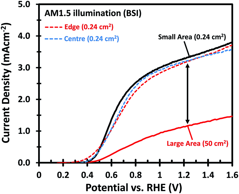 | ||
| Fig. 1 The current density–voltage (J–V) curves of a small area (1 × 2 cm2) W:BiVO4 photoanode with an illuminated area of 0.24 cm2 (black), compared to the large area (7 × 12 cm2) W:BiVO4 photoanode with an illuminated area of 50 cm2 (red). The dashed curves show the J–V plots from the small W:BiVO4 pieces (1 × 2 cm2) cut from the centre and edge of the 50 cm2 sample, with an illuminated area of 0.24 cm2. The electrolyte consists of 0.5 M Na2SO3 and 0.1 M KPi buffer in deionized water with pH of 7. BSI: back-side illuminated. | ||
The drop in the photocurrent is presumably caused by ohmic losses in the system due to e.g. resistance of the FTO substrate, finite conductivity of the electrolyte solution, and/or contact resistance(s). Since detailed modeling of these losses typically requires 2D numerical calculations, we first consider a simple model that captures all losses in the form of a single internal resistance, Rint. Using this model, which is described in more detail in ESI Note S1,† and assuming that the photocurrent density is the same everywhere and equal to that of the small area sample of Fig. 1, we calculated the expected photocurrent for a 50 cm2 photoelectrode for different values of Rint. The results are shown in Fig. 2. The curves show a reasonable overlap with the measured data for an actual 50 cm2 BiVO4 photoelectrode (solid red curve) for an internal resistance value of ∼10 Ω. At a potential of 1.23 V vs. RHE the voltage loss in the 50 cm2 photoanode is about 0.6 V (see arrow in Fig. 2), consistent with current density at this potential (1.2 mA cm−2 × 50 cm2 × 10 Ω ≈ 0.6 V).
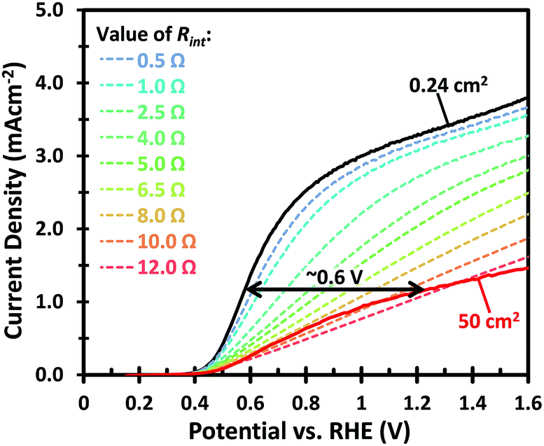 | ||
| Fig. 2 The J–V curves of small (solid black) and large (solid red) W:BiVO4 photoanodes measured in 0.5 M Na2SO3 + 0.1 M KPi pH 7 buffer under AM 1.5G illumination. These curves are compared with the calculated J–V curves of a 50 cm2 W:BiVO4 photoanode (dashed lines) with the same performance as the small area sample, but subjected to different resistances from 0.5 to 12 Ω. | ||
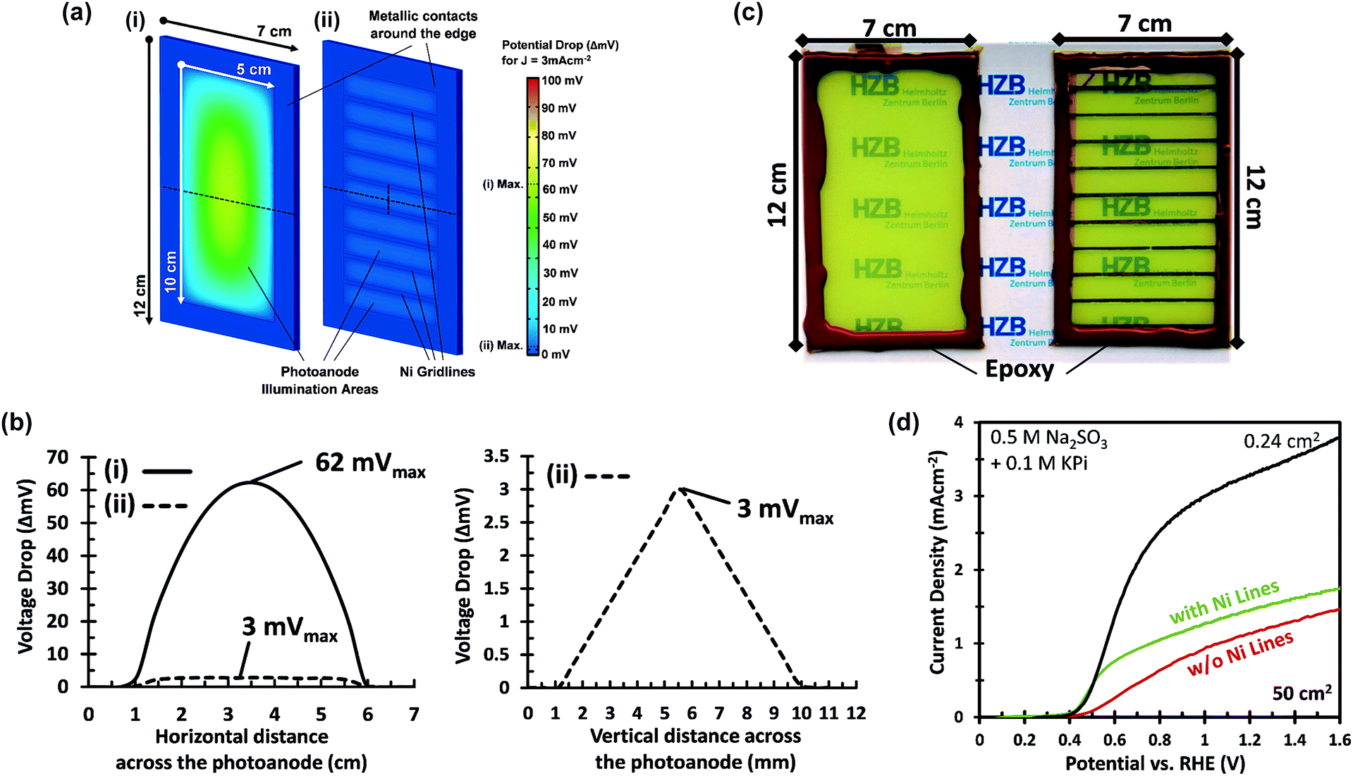 | ||
| Fig. 3 (a) Colour gradient plots of the simulated potential distribution across a 5 × 10 cm2 photoanode (i) without and (ii) with Ni lines for a photocurrent density of 3 mA cm−2, and (b) shows the graphical plots of the potential drop at different points across the photoanodes (dashed lines in Fig. 3a). (c) Photographs of two 50 cm2 area W:BiVO4 photo-anodes, (i) without and (ii) with Ni lines. (d) J–V curves of the corresponding photoanodes in an electrolyte containing 0.5 M Na2SO3 and 0.1 M KPi buffer of pH 7, with backside AM1.5G illumination (BSI). | ||
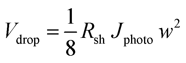
A voltage loss of 62 mV in the FTO is not negligible and mitigation of this loss would still be useful, especially when the area of the photoanode is increased beyond 50 cm2 and higher photocurrent densities are considered. Our calculations fall in line with what has been previously reported for the resistive losses caused by large area FTO substrates.36 This problem has also been encountered in photovoltaic cells, where the sheet resistance of FTO used as a top contact layer is too high for efficient current collection.37 This is typically resolved by depositing highly conductive metallic busbars on the front contact of the PV cells. Since these metallic busbars partially block light from reaching the PV junction, a tradeoff has to be made between optical exposure and current collection by optimizing the thickness, spacing, and pattern of the grid lines. Taking the same approach as in photovoltaics, we investigated the deposition of conductive lines to overcome the ohmic losses in the substrate. The maximum potential drop in the middle between two metallic lines, Vdrop, is a function of the FTO sheet resistance, Rsh, the photocurrent density, Jphoto, and the distance between metallic lines, w, and can be estimated using eqn (1).
 | (1) |
This equation, which is derived in ESI Note S3,† assumes that the generated photocurrent density is the same everywhere and that edge effects can be ignored. Calculated values of the potential drop for different line spacings and current densities are shown in Fig. S5.† To limit the potential drop to <5 mV at photocurrent density of 3 mA cm−2, the metallic lines need to be separated by about 1 cm. We have also simulated the distribution of this potential drop using the DC conductivity model (Fig. 3a and b). Indeed, the addition of metallic lines spaced 0.9 cm apart results in a maximum potential drop of only ∼3 mV at 3 mA cm−2.
Based on these calculations, 200–300 nm thick Ni lines with a 2 mm width and a spacing of 9 mm were electrodeposited onto the FTO substrates prior to deposition of the W:BiVO4 layer (Fig. 3c). The resistance of the Ni lines, measured over a distance of 2 cm, is ca. 1.5 Ω and did not change significantly after annealing at 450 °C (Fig. S6†). As shown in Fig. 3d, a significant improvement is observed at low photocurrents, just above the onset potential. At photocurrents beyond 0.8 mA cm−2 the improvement becomes less pronounced, which suggests that another process becomes performance-limiting at these current densities (see section 2.2). The Ni lines improve the average AM1.5G photocurrent by ca. 30% to 1.5 mA cm−2 at 1.23 VRHE. Despite this improvement, the photocurrent is still a factor of 2 below the photocurrent density for the small area sample. It is important to consider that under back side illumination, the Ni lines block light from reaching the W:BiVO4 layer. This effectively renders the area covered by the Ni lines inactive. For an average sample, we deposited 9 Ni lines (∼0.2 × 5 cm2 each) within the active area of the photoanode, which decreases the total active area from 50 cm2 to 41 cm2. Note, however, that we always use a value of 50 cm2 for calculating the photocurrent density. This corresponds to the ‘designated illumination area’.38 The reported values are thus conservative, and can be significantly improved by optimizing the geometry of the Ni lines. This is, however, beyond the scope of this study.
To investigate whether the uniformity of the large area W:BiVO4 photoanodes is affected by the deposition of Ni lines, different parts of the electrode were masked. As shown in Fig. 4, the 5 × 10 cm2 samples were divided into four equal parts of 12.5 cm2 each. The AM1.5G photocurrents of each part are shown in Fig. 4, and the variation between the samples remains minimal (less than ±13%). Interestingly, even with a smaller illumination area (12.5 cm2) the measured photocurrent density is still close to 1.5 mA cm−2, matching that of the large area under full illumination (50 cm2). This implies that other factors not yet considered limit the photocurrent density, which will be discussed in the next section.
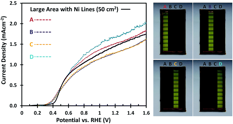 | ||
| Fig. 4 AM1.5G J–V curves for the W:BiVO4 photoanodes with Ni lines, measured on 4 different areas of the sample (right, A–D) to determine the uniformity of the photocurrent across the large area sample, with an electrolyte containing 0.5 M Na2SO3 and 0.1 M KPi buffer of pH 7. | ||
2. PEC performance of 50 cm2 BiVO4 photoanode for water oxidation
One major difference between the measurements for the small and large area samples is the size of the photoelectrochemical cell used. The larger volume may lead to higher ohmic losses in the electrolyte and less efficient transport of the ionic species relevant for the oxygen evolution reaction (i.e., H+ or OH−). To investigate this, the photoanodes in this section are modified with CoPi and measured in a 2.0 M KPi buffer (without hole scavenger) in order to ensure efficient charge transfer and fast water oxidation kinetics.6,39–41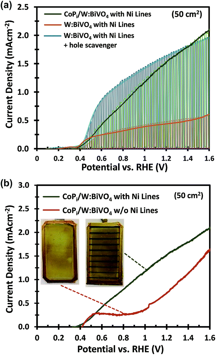 | ||
| Fig. 5 (a) J–V curves under constant, dark and chopped AM 1.5G illumination comparing the performance of large area (50 cm2) W:BiVO4 photoanodes with Ni lines, either in 2.0 M KPi buffer solution with 0.5 M Na2SO3 (blue), or without hole scavenger, before (orange) and after (green) photo-electrodeposition of CoPi. (b) J–V curves comparing CoPi-modified W:BiVO4 photoanodes with (green) and without (red) Ni lines measured in 2.0 M KPi buffer, pH 7, under AM 1.5G illumination. Inset: photographs of the CoPi deposited on W:BiVO4 photoanodes without (left) and with (right) Ni lines. | ||
The importance of the Ni lines during the photoelectrodeposition of CoPi is illustrated in Fig. 5b. Without Ni lines, we obtained a rather poor coverage quality of CoPi (see inset of Fig. 5b), which subsequently results in a poor water oxidation performance. The coverage of CoPi is very much improved with Ni lines. We speculate that the improved homogeneity of CoPi is arising from the uniformity of the potential drop across the substrates with Ni Lines. At the initial stage of CoPi photo-electrochemical deposition, we observe a large spike in the anodic photocurrent density for all samples, as is typical for photoelectrodeposition of CoPi.42,43 This initial photocurrent contributes significantly to the nucleation and growth of CoPi. As confirmed in Fig. 3a and b, at relatively high current densities (>3 mA cm−2), a potential drop >70 mV can be expected within the central region of the samples without Ni lines. Such a potential drop could inhibit CoPi nucleation and therefore lead to the non-uniform deposition of CoPi in these large area samples. Interestingly, the distribution of CoPi deposited on the samples without Ni lines (inset of Fig. 5b) closely resembles the color gradient plots of the potential distribution across a 5 × 10 cm2 photoanode without Ni lines (see Fig. 3a). We therefore conclude that the combination of (i) applying Ni lines to the FTO substrate and (ii) photoelectrodeposition of CoPi is essential to improve the photocurrent of large area W:BiVO4 photoanodes for water oxidation.
To better understand the role of electrolyte conductivity, we first measured the specific conductivities for a series of KPi electrolytes at pH 7 as a function of concentration (Fig. S10†). The conductivity values in Fig. S10† are consistent with previously reported values for these electrolytes.45 The electrolyte conductivity shows a non-linear increase with electrolyte concentration, especially at higher concentration. The non-linearity is caused by the increasing interaction between the ions, resulting in a decrease in molar conductivity with increasing concentration.46
Fig. 6 shows the photocurrent measured at 1.23 VRHE as a function of electrolyte concentration for the small and large area CoPi/W:BiVO4 photoanodes, normalized to the photocurrent measured in 0.1 M KPi. For the small area electrode, it is clear that KPi concentrations from 0.1 M to 2.0 M have no effect on the overall photocurrent. This indicates that a 0.1 M KPi buffer solution provides sufficient ionic conductivity for small area PEC cells (<1 cm2), even at neutral pH. For the large area electrode, on the other hand, the photocurrent is found to increase with increasing electrolyte concentration. This correlation is not specific to phosphate buffer, since a similar dependence was also observed when measurements were performed in sodium sulfate (Na2SO4) electrolyte (see Fig. 6). In KPi buffer, the photocurrent can be improved by 40% by simply increasing the KPi concentration from 0.1 M to 2.0 M. Concentrations of KPi greater than 2.0 M were not used in this investigation, since the saturated solution would rapidly precipitate on the walls of the cell and bubbles would begin to stick to the electrodes.
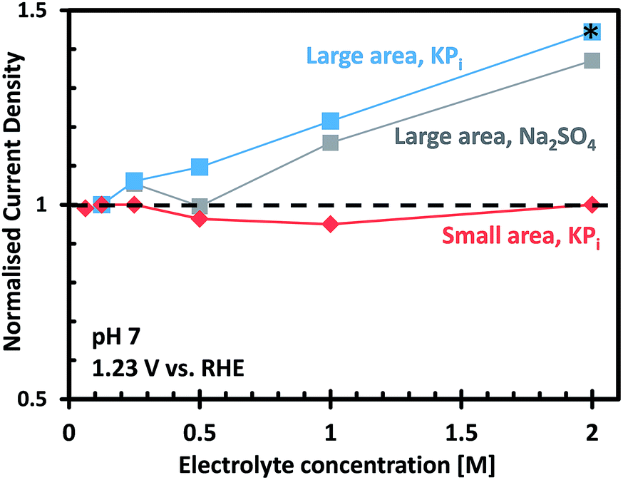 | ||
| Fig. 6 Normalized photocurrent measured at 1.23 VRHE, under AM 1.5G illumination, for the small and large CoPi/W:BiVO4 photoanodes as a function of concentration of electrolyte (pH 7). Zero concentration corresponds to pure deionized water. *Electrolyte selected for all measurements using the large area BVO4 without hole scavenger. | ||
Using the measured electrolyte conductivity of the KPi buffer, the potential drop between a 50 cm2 BiVO4 photoanode and the Pt counter electrode can be estimated using a simple iR model. The average distance between the working and counter electrodes in our large area PEC cell, shown in Fig. S11,† is estimated to be 3 cm. This leads to an overall potential drop across the electrolyte of ca. 600 mV for a 0.1 M KPi solution (15 mS cm−1) and a photocurrent density of 3 mA cm−2. In contrast, when a 2 M KPi solution is used with a conductivity of 130 mS cm−1, the potential drop decreases by almost an order of magnitude to ca. 69 mV. Despite the improvements by the deposition of Ni lines and increasing the electrolyte concentration, the photocurrent of the large area W:BiVO4 (1.5 mA cm−2 at 1.23 VRHE) is still well below its small area equivalent. Our calculations indicate that the remaining ohmic losses for photoanodes with Ni lines in 2 M KPi electrolyte would amount to approximately 3 + 69 = 72 mV for a photocurrent density of 3 mA cm−2; this voltage drop cannot explain the photocurrent difference between the small and large area electrode. Instead, we tentatively attribute this discrepancy to the low concentration (∼10−7 M) of H+/OH− species at neutral pH. At such low concentrations, diffusion of these species cannot keep up with the rate at which they are generated (H+) and consumed (OH−), resulting in local enhancement and depletion, respectively, of these species. This results in a local decrease of the pH near the photoanode surface and a corresponding positive shift of the Nernst potential of the oxygen evolution reaction that will lead to a decrease in photocurrent. We note that in the KPi buffer electrolyte, due to the low concentration of OH−, the actual species that is oxidized is water,47 resulting in the formation of protons that have to diffuse away from the surface. Moreover, the transport of H+/OH− is essentially governed by the movement of buffer components (i.e., the H2PO4− and HPO42− ions); the term “effective H+/OH− conductivity” would therefore be more appropriate here.
To further confirm that H+/OH− transport limits the performance, we performed two-electrode electrochemical water splitting experiments in the dark. We used two sets of identical Pt-coated FTO electrodes, one set with a surface area of 0.24 cm2 for each electrode, and one set with a 40 cm2 electrode area. The large-area FTO/Ag/Pt electrodes are highly conducting, with a resistivity that is ca. 60 times smaller than that of bare FTO (Fig. S12†). The two electrodes in each set are placed in a large beaker and are oriented parallel to each other, separated by a distance of 2 cm (see Fig. 7a and S13†). For each set of electrodes, we measured the J–V curves in 2.0 M KPi (pH 7) and in 0.6 M KOH (pH 13). The KOH concentration was chosen to ensure that the total electrolyte conductivity is the same as that of the 2.0 M KPi (130 mS cm−1). The results are shown in Fig. 7a. For the large-area electrodes, the pH 7 electrolyte (solid red curve) requires much higher overvoltages than the pH 13 solution (dashed red curve). Using eqn (1), the voltage drop within the FTO/Ag/Pt electrodes is calculated to be less than 23 mV for a current density of 10 mA cm−2. This shows that most of the voltage drop occurs in the electrolyte. This is indeed consistent with hypothesis that a low concentration of H+/OH− limits the water splitting current.
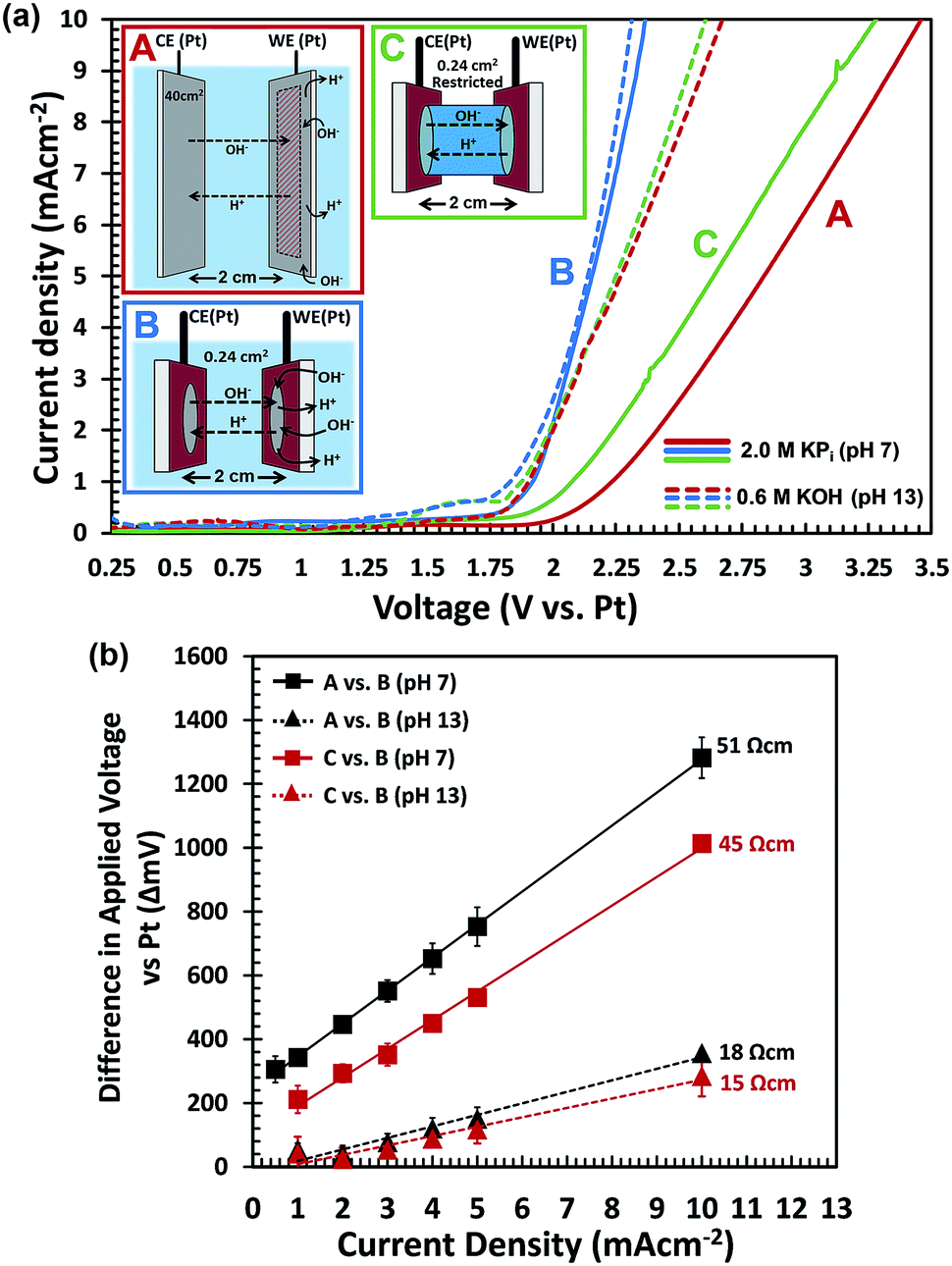 | ||
| Fig. 7 (a) Voltammograms for water splitting in a two-electrode setup, using two identical Pt electrodes in three different configurations (A–C) and in two different electrolytes: 2.0 M KPi, pH 7 (solid curves) and 0.6 M KOH, pH 13 (dashed curves) using a scan rate of 10 mV s−1. The inset shows the three different cell configurations in which the two Pt electrodes are oriented parallel to each other and separated by 2 cm. A: large area Pt electrodes in a large electrolyte volume, B: small area Pt electrodes in a large electrolyte volume and C: small area Pt electrodes in a restricted cell volume. (b) Additional overvoltages needed to achieve a certain current density for (black squares) (A) vs. (B) in 2.0 M KPi (pH 7), (black triangles) (A) vs. (B) in 0.6 M KOH (pH 13), (red squares) (C) vs. (B) in 2.0 M KPi (pH 7), and (red triangles) (C) vs. (B) in 0.6 M KOH (pH 13). Data points follow a linear fit and error bars indicate standard deviations of 5 repeated measurements. The resistivities (in Ω cm) were calculated from the slopes of the curves divided by the distance between the electrodes (2 cm). | ||
For the small-area electrode, the results seem counter-intuitive at first; the J–V curves almost overlap for the pH 7 and pH 13 solutions (solid and dashed blue curves, respectively). This can, however, be understood when realizing that the radius of the electrodes (∼0.3 cm) is much smaller than the distance between them (2 cm). This means that for the pH 7 measurement, the OH− species can be replenished from the surrounding electrolyte,48,49i.e., the bulk electrolyte volume beyond the cylindrical volume between both electrodes (Fig. S13B†). To verify this, we constructed a cell in which the electrolyte was restricted to the cylindrical volume between the two small-area electrodes (Fig. S13C†). The resulting J–V curves for the ‘restricted’ configuration are shown in green in Fig. 7a. In contrast to the ‘unrestricted’ configuration, the J–V curve recorded in the pH-neutral KPi electrolyte (solid green curve) shows a much larger overvoltage than the measurement in 0.6 M KOH (dashed green curve). The pronounced differences between the restricted and unrestricted curves provides direct evidence that diffusion of OH− species from the surrounding electrolyte mitigates the depletion of OH− species and leads to a reduction in the required overvoltage.
It should be noted that even at pH 13, the restricted configuration (dashed green curve) shows a few tenths of a volt more overvoltage than the unrestricted configuration (dashed blue curve). This indicates that even at these high pH values and relatively modest current densities, depletion of OH− can become an issue. While further increase of the pH will help to mitigate this, it may also lead to corrosion of the (photo)electrode. A better strategy would be to decrease the distance between the electrodes and/or to reduce the electrode area-to-electrolyte volume ratio in order to facilitate the replenishment of OH− from the surrounding electrolyte.
To visualize the data from Fig. 7a in a different manner, we plotted the differences in required overvoltages under various conditions as a function of current density (Fig. 7b). The black curves show the additional overvoltage needed when scaling a small area electrode to a large area at pH 7 and at pH 13. The difference in slopes show that the resistive losses for scale-up to 50 cm2 are ∼3 times higher at pH 7 than at pH 13, despite the fact that both electrolytes have the same total ionic conductivity (130 mS cm−1). The red curves show the additional overvoltage needed when ‘restricting’ the electrolyte volume around a small area electrode at pH 7 and at pH 13. The difference in slope for both pH values is again a factor of 3. The perfectly linear slopes of all curves in Fig. 7b confirm that the voltage losses due to scale-up and restriction of the electrolyte volume are purely resistive in nature. This is consistent with the notion that these losses are due to mass transport limitations of OH−. One unexpected observation is that not all curves in Fig. 7b go exactly through the origin, which is what one would expect for purely resistive losses. We attribute this to slight variations in the concentration of dissolved oxygen gas during the experiments. This induces Nernstian shifts in the potentials of the electrochemical half-reaction which affects the onset potential of the current–voltage curves.
Interestingly, the additional resistivity introduced by restricting the electrolyte volume in a small area cell at pH 13 is comparable to the resistivity introduced by scale-up of this same cell from 0.24 cm2 to 50 cm2 at the same pH (red vs. black triangles in Fig. 7b). This clearly shows that diffusion (or lack thereof) of OH− species from the surrounding electrolyte can have a profound influence on the resistive losses in the system.
These results again show that the depletion of H+/OH− at the surface of the electrodes—as a result of the low initial concentration (neutral pH) and restricted diffusion from the surrounding electrolyte—is the main cause of efficiency losses when scaling up small area electrodes. A possible engineering approach to avoid such limitations is to divide a single large-area electrode into multiple segments in order to optimize flow patterns and avoid undesired pathways for ionic species.50,51
Finally, although not demonstrated here, we note that the moderate electrolyte conductivity may also result in a spatial distribution of the surface potential across the large area BiVO4 photoanodes, known to further limit the PEC performance of large area photoelectrodes. Hankin et al. recently reported that without an appropriate electrode configuration and electrolyte conductivity, a 10 × 10 cm2 hematite (α-Fe2O3) photoanode would exhibit inhomogeneous spatial distribution of surface potentials and current densities. This would be detrimental to the resultant hydrogen/oxygen evolution efficiencies. It was also stated that for α-Fe2O3 photoanodes with an area of 10 × 10 cm2, an electrolyte concentration in excess of ≥1 M KOH would be required.28
3. Unassisted PEC–PV water splitting devices
In the previous sections we have outlined our efforts to improve the PEC performance of large area W:BiVO4 photoanodes and minimize the discrepancy with the small area samples. The next step is to integrate these large-area photoanodes into complete PEC–PV water splitting devices.The W:BiVO4 photoanodes was placed in front of series-connected silicon heterojunction (SHJ) solar cells (positioned side-by-side), each with an area of 25 cm2. In this stacked configuration, the light interacts with the different device components in the following order upon entering: glass/FTO/BiVO4/CoPi/electrolyte/glass/SHJ. The advantage of this configuration is that the BiVO4 electrode is illuminated via the back side, which gives higher photocurrents than front-side illumination.6,52,53
Furthermore, the Pt mesh counter electrodes were placed at both sides of the photoanodes outside of the light path and were connected to the n-terminal of the SHJ solar cells. The two-electrode J–V curves of the 50 cm2 CoPi/W:BiVO4 photoanode and of the series-connected SHJ cells (placed behind the BiVO4 electrode) are shown in Fig. 8a. From the intercept of these individual curves, an operating photocurrent of 1.5 mA cm−2 at ca. 1.23 V is expected. Indeed, the measured short-circuit photocurrent density (at zero bias) of the integrated device is ca. 1.5 mA cm−2, as shown in Fig. 8b. This corresponds to an STH efficiency of 1.9%.
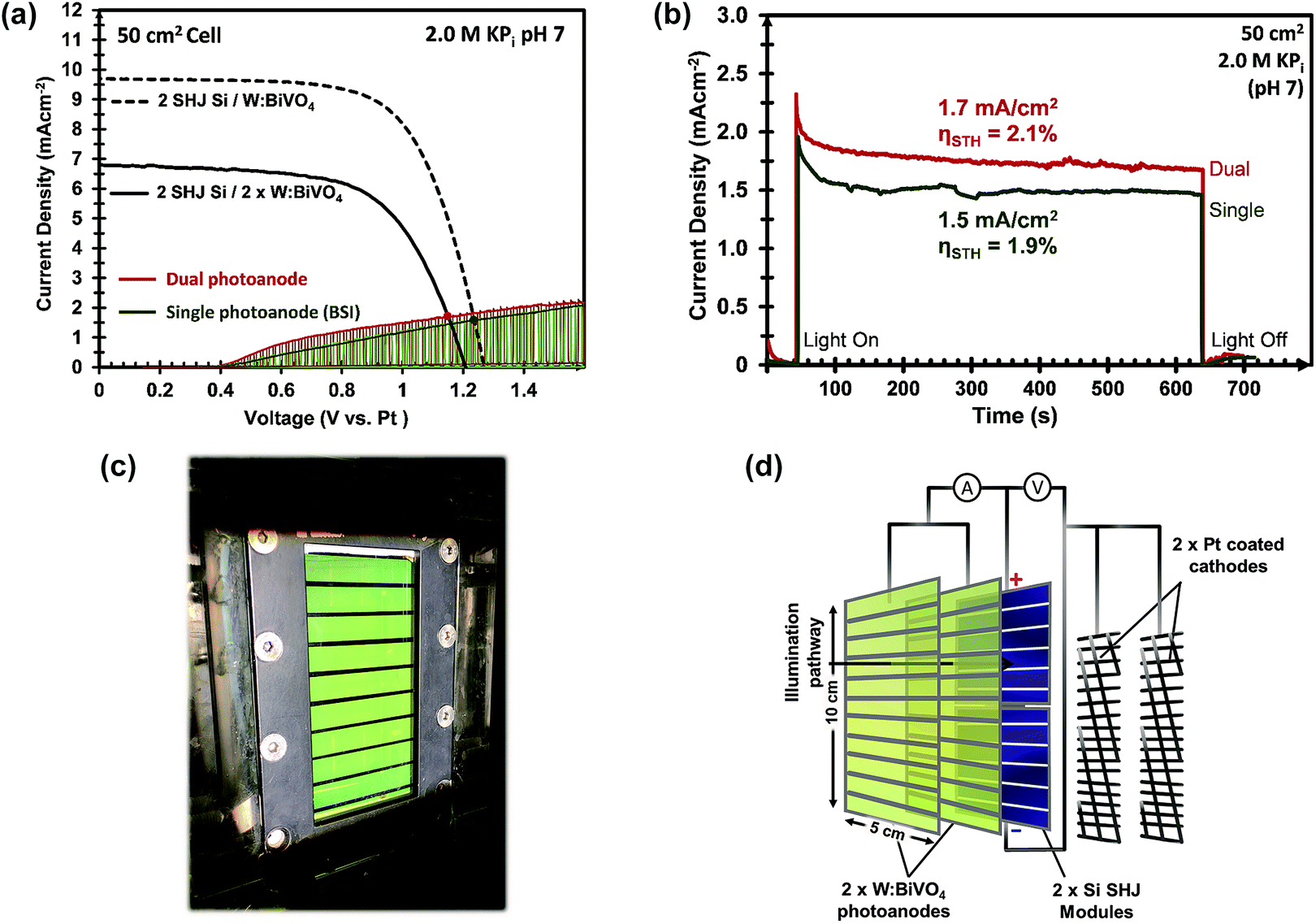 | ||
| Fig. 8 (a) J–V curves for the 50 cm2 2× SHJ PV module behind single (dashed black lines) or dual (solid black lines) W:BiVO4 photoanodes, and J–V curves for the 50 cm2 single (green) and dual (red) W:BiVO4/CoPi photoanodes under chopped AM 1.5G illumination. (b) Current density and voltage vs. time for the 50 cm2 PEC–PV devices with single (green) and dual (red) photoanode configurations over 10 min. All measurements were conducted in a stirred 2.0 M KPi electrolyte at pH 7. (c) Photograph of the large area (50 cm2) integrated PEC–PV device in the dual photoanode configuration with a device structure of W:BiVO4(BSI)/Electrolyte/W:BiVO4(FSI)/2SHJ-PV/2Pt, illustrated in (d). BSI: back-side illuminated, FSI: front-side illuminated. | ||
Our PEC cell configuration also allows for the use of two stacked BiVO4 photoanodes in conjunction with the PV cells. In this so-called “dual photoanode” configuration the total amount of light absorbed by the BiVO4 is distributed over two photoanodes, which offers a solution for the usual trade-off between optical absorption and carrier diffusion length in metal oxide photoelectrodes.15 As shown in Fig. 8c and d, the PEC–PV cell employs the first CoPi/W:BiVO4 layer as the front window of the cell (back-side illuminated, BSI), and the second CoPi/W:BiVO4 layer as its back window (front-side illuminated, FSI), with the Si solar cells also attached to this back window. The second BiVO4 photoanode provides an additional photocurrent of 0.21 mA cm−2 at 1.23 VRHE, which originates from the remaining supra-bandgap photons that were not absorbed by the first W:BiVO4 photoanode. The two-electrode J–V curve of the dual CoPi/W:BiVO4 photoanode is also shown in Fig. 8a (red curve); a ca. 10% improvement is obtained by the dual photoanode configuration. This results in an average operating photocurrent density of ca. 1.72 mA cm−2 (Fig. 8b). This corresponds to an STH efficiency of 2.1%, which, to the best of our knowledge, represents a new performance record for a large area (>10 cm2) solar water splitting PEC–PV device based on metal oxide photoelectrodes.
To illustrate the significance of the BiVO4 photoanodes to the overall device performance, a cell consisting of a Pt cathode/2 series-connected SHJ/Pt anode was also tested. Upon direct illumination to the SHJ cells, only a negligible photocurrent and STH efficiency (<0.1%) was achieved. Table 2 summarizes the key performance characteristics for the different PEC–PV configurations under AM 1.5G illumination.
| PEC–PV Configuration | Illum. Area (cm2) | J (mAcm−2) | I (mA) | Average. STH Efficiency. (%) |
|---|---|---|---|---|
| Pt/2-SHJ/Pt | 50 | 0.02 | 1.0 | 0.03 |
| CoPi/W:BiVO4(FSI)/2-SHJ/Pt | 50 | 1.00 | 50.0 | 1.2 |
| CoPi/W:BiVO4(BSI)/2-SHJ/Pt | 50 | 1.50 | 75.0 | 1.9 |
| Dual-CoP i /W:BiVO4/2-SHJ/Pt | 50 | 1.72 | 86.0 | 2.1 |
| Dual-CoP i /H,W:BiVO4(FSI)/2-SHJ/Pt | 0.24 | 4.45 | 1.07 | 5.5 |
| Dual-CoPi/H,W:BiVO4(FSI)/3-SHJ/Pt | 0.24 | 5.12 | 1.23 | 6.3 |
Current density vs. time measurements (Fig. 8b) showed that both the single and dual photoanode devices displayed pronounced transients during the first 100–200 s, after which the photocurrent remains relatively stable. During these measurements the formation of bubbles at the electrodes could be clearly observed (see Video in the ESI†). The electrolyte required constant agitation with N2 purging in order to release the bubbles from the surface of the electrodes and to prevent them from scattering the light away from the series-connected Si PV cells (and the second photoanode). Without this N2 purging and agitation, the photocurrent drops rapidly within the first 1–2 min of operation due to rapid bubble formation that block the optical pathway to the back electrode and PV (second W:BiVO4 and Si PV). These observations show that a full recirculation system is needed for long-term operation of the device. Long term stability measurements of the single and dual large area PEC–PV devices, presented in Fig. S14,† shows a turbulent (due to N2 bubbling), and relatively stable photocurrent density for up to 7 hours. The total amount of photo-generated charge that passed during these experiments exceeds the amount needed to photo-corrode the 200 nm BiVO4 film by a factor of ∼110 (assuming 8 holes are needed to photo-dissolve one BiVO4 unit), and exceeds the amount of charge needed to deposit the CoPi by a factor >600. This means that the faradaic efficiency is >99%.
It should be noted that the efficiencies mentioned above do not take into account chemical recombination due to crossover of oxygen to the cathode side. Since no membrane was used, crossover will indeed occur, which would lower the actual solar-to-hydrogen efficiency. However, this does not affect the STH values determined from the measured photocurrent.
In an attempt to further improve the efficiency, we used a hydrogen annealing treatment for the BiVO4 photoelectrodes. We recently reported that a mild hydrogen treatment (300 °C anneal in 2.4% H2/Ar for 10 minutes) effectively enhances the charge carrier lifetime in BiVO4 photoanodes.54 Applying the same hydrogen treatment to a small area W:BiVO4 photoanode also results in significant improvement of the photocurrent, as shown in Fig. 9a; AM1.5G photocurrent of 4.0 mA cm−2 was achieved at 1.23 VRHE for the hydrogen-treated tungsten-doped BiVO4 (H,W:BiVO4). By combining two CoPi/H,W:BiVO4 electrodes in a dual photoanode configuration with 2 series-connected SHJ solar cells, a 0.24 cm2 PEC–PV device with an operating photocurrent of 4.5 mA cm−2 is achieved (Fig. 9b). This corresponds to an STH efficiency of 5.5%, which is amongst the highest reported efficiencies for an oxide-based solar water splitting device (Table 1). Combination with three series-connected SHJ cells gave an even higher efficiency of 6.3%. It should be noted that three series-connected SHJ cells can split water even without the BiVO4 photoanodes (Fig. S15†), albeit at lower efficiency (3.08 mA cm−2 ≈ 3.8%).
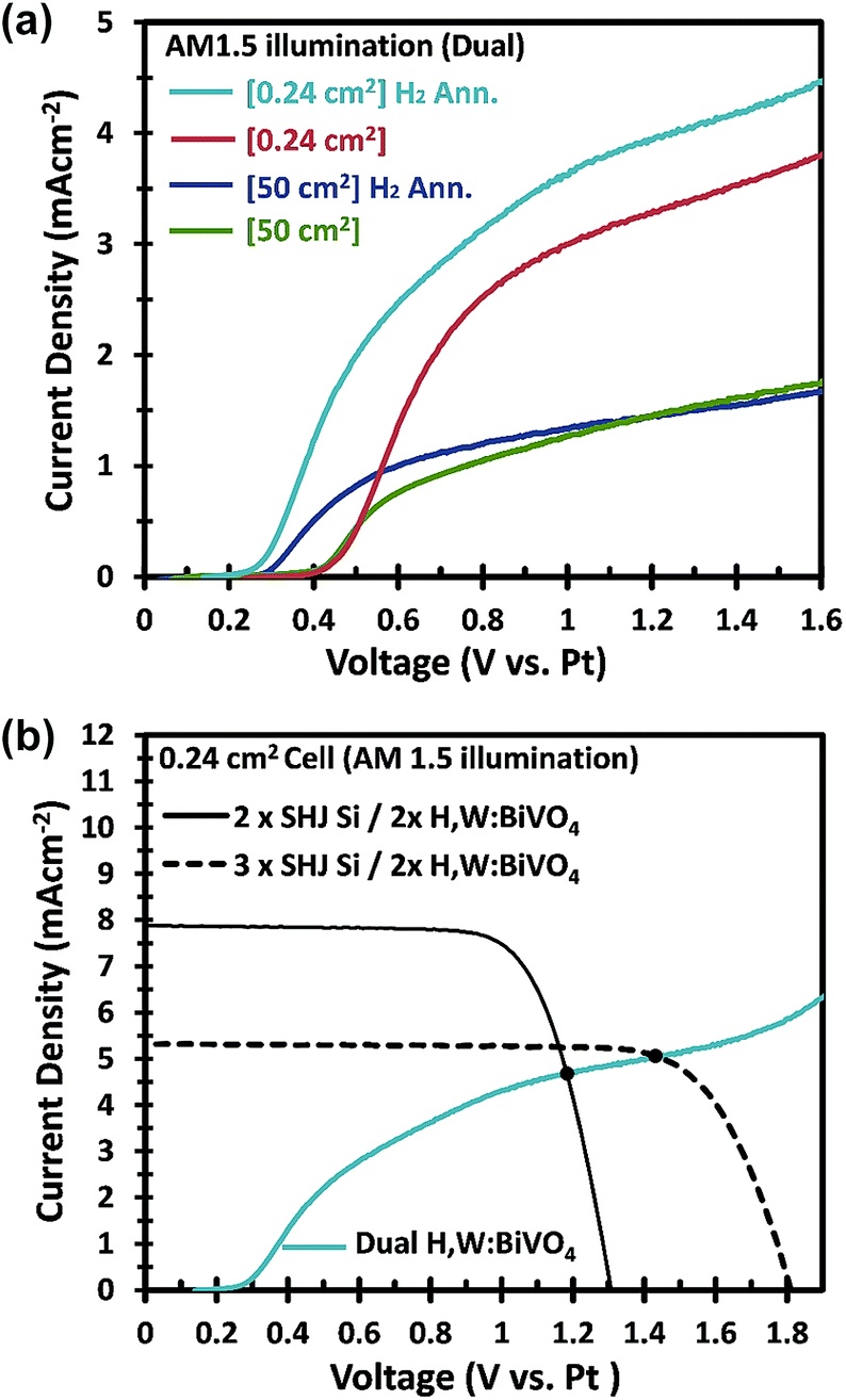 | ||
| Fig. 9 (a) J–V curves comparing the effects of hydrogen annealing on the small and large area dual-CoPi/W:BiVO4 photoanodes in 0.1 M KPi (small area) or 2.0 M KPi (large area) buffer. Large area samples are with Ni lines. (b) J–V curves of a small area 2 SHJ PV (black line) and the 3 SHJ PV (dashed black line) with dual-CoPi/H,W:BiVO4 photoanodes as the front windows, and the small area dual-CoPi/H, W:BiVO4 photoanode, measured in 0.1 M KPi buffer. | ||
Hydrogen treatment of the large-area BiVO4 photoanodes was done in a rapid thermal processing (RTP) system, since the electrodes do not fit in our regular tube furnace. Although the onset potential is shifted cathodically (see Fig. 9a), the photocurrent at 1.23 VRHE does not improve with hydrogen treatment. Further optimization of the RTP process is needed in order to obtain the same level of improvement as for the small area BiVO4 photoanodes.
Conclusions
In summary, we have demonstrated a large area (50 cm2) PEC–PV water splitting device based on a W:BiVO4 top absorber and a silicon heterojunction bottom absorber and discussed the challenges encountered during scale-up of this system. Spray pyrolysis was used to fabricate 50 cm2 W:BiVO4 photoanodes of uniform thickness and quality. However, the photoelectrochemical performance of the large area photoelectrode was significantly lower than the small area equivalent. We found that only 10% of the voltage drop in the large area system is due to ohmic losses in the FTO substrate, while using a 2.0 M instead of 0.1 M buffer concentration in the electrolyte can increase the photocurrent by up to 40%. Both of these factors do not affect the performance of the small area electrode. We mitigated these losses by depositing metallic Ni lines onto the FTO substrate prior to the W:BiVO4 deposition and by increasing the electrolyte (KPi buffer) concentration. The Ni lines significantly improved the uniformity of the electrodeposited CoPi and resulted in an AM1.5 photocurrent of ∼1.5 mA cm−2 at 1.23 V vs. RHE for a 50 cm2 CoPi/W:BiVO4 photoelectrode. The main bottleneck, however, is the low concentration of H+/OH− reactant species in pH-neutral solutions. This leads to poor conductivity and rapid depletion of these species in the electrolyte, which causes pH changes and potential drops up to 500 mV at a current density of 3 mA cm−2. Despite these losses, a STH efficiency of 2.1% was achieved for a combination of two large area CoPi/W:BiVO4 photoanodes in a dual photoanode configuration, connected in tandem to two series-connected SHJ solar cells. Although this efficiency is the highest reported thus far for large area (>10 cm2) unassisted solar water splitting based on metal oxide photoelectrodes, it is still a factor of 3 lower than the 5.5% STH efficiency that we achieved in this study for the corresponding small area device. Reduction of these scale-up losses requires either strongly acidic or alkaline solutions to avoid local pH gradients, or innovative engineering solutions in the device design that allows the use of pH-neutral solutions.Experimental
4. Masking and pre-treatment of the large area FTO substrates
Prior to electrodeposition, the 7 × 12 cm2 TEC 7™ FTO substrates were cleaned thoroughly with soapy water (10 vol% Triton-X™), ethanol, and then dried under a flow of compressed N2. The substrates were then masked with Kapton® tape for the deposition of 7 cm long, 2 mm wide conducting Ni lines. The lines were separated by the width of the tape (0.9 cm). To improve the adhesion of the electrodeposited Ni lines, the masked FTO substrates were treated with a chemical reduction process, described in more detail elsewhere.55,56 Briefly, masked FTO substrates were immersed in 1.0 M glycine (≥99%; Aldrich), 0.5 M FeSO4·7H2O (≥99%; Aldrich) in deionized water was adjusted to a pH ∼2.5 using H2SO4 and NaOH. The masked FTO substrates were immersed in the solution horizontally for 3 min (FTO-side facing upwards). Zn powders (mesh 100) were then uniformly dispersed over the FTO and allowed to settle on the surface for 10 min, during which hydrogen bubbles evolved. The substrates were then removed and washed with a fast jet of deionized water. This resulted in the formation of a shiny adherent intermetallic film consisting of FexSny on the surface of the unmasked regions of the FTO.5. Electrodeposition of Ni lines
The electrochemical deposition of Ni lines was performed in a three-electrode electrochemical cell using a VersaSTAT 3 potentiostat/galvanostat (Ametek). The pre-treated masked FTO acted as the working electrode and a Pt wire served as the counter electrode. An Ag/AgCl reference electrode was used (XR300, saturated KCl, Radiometer Analytical). Ni was electrochemically deposited under galvanostatic conditions at a current density of −5 mA cm−2 (an absolute current of −50 mA for our typical masked FTO sample) for 900 s. The electrochemical bath was composed of 1.14 M NiSO4·7H2O (≥98%, Aldrich), 0.16 M NiCl2·6H2O (≥98%, Aldrich), and 0.73 M H3BO3 (≥99.5%, Aldrich) in deionized water (>18 MΩ cm). The bath was heated to 50 °C and stirred during the electrochemical deposition. After the deposition, the Kapton tape was removed and the FTO with Ni lines were ultrasonically cleaned in deionized water, acetone, and ethanol, each for 60 s, then dried under a fast jet of N2.6. Fabrication of W-doped BiVO4 photoanodes
First, a ∼10 nm thick tin oxide (SnO2) layer was deposited onto cleaned FTO substrates (with or without Ni lines) by spray pyrolysis using a solution of 0.1 M SnCl4 in ethyl-acetate. The substrate temperature was 450 °C. Subsequently, ∼200 nm thick BiVO4 photoanodes with 1% W doping were deposited by spray pyrolysis using a previously reported precursor solution consisting of 4.44 mM Bi(NO3)3·5H2O (98%, Sigma-Aldrich), 4.44 mM VO(C2H7O2)2 (99%, Alfa Aesar) and 0.044 mM W(C2H5O)6 from 5% w/v in ethanol (99.8%, Alfa Aesar).6 The solvent consists of a 10 vol% of acetic acid in absolute ethanol. For the fabrication of 0.24 cm2 photoanodes a spray rate of 1–1.5 mL per spray cycle was used. For the 50 cm2 photoanodes, the spray rate was adjusted to 2–2.5 mL per spray cycle by increasing the carrier gas pressure. The increase in spray rate enlarged the area covered by the mist generated by the spray nozzle, and ensured a homogeneous deposition over larger areas (Fig. S7†). Each spray cycle consisted of 5 s of spraying, followed by a 55 s of pause to allow solvent evaporation. This cycle was repeated 180 times using a home built automatic spray controller. The overall volume of precursor used was ∼180 mL for a 0.24 cm2 sample and ∼360 mL for a 50 cm2 sample. Special precautions had to be taken to prevent cracking and damage to the large area substrates. Specifically, the substrates were heated to 450 °C at a slow ramp rate of 5 °C min−1. Furthermore, droplet formation around the edge of the substrate was a major cause of large area substrate breakage/cracking and this could be avoided by positioning the nozzle 20 cm above the substrate. After deposition the samples were cooled gradually to room temperature by turning off the heater plate, followed by annealing in air (box furnace) for 2 hours at 460 °C, using a heating rate of 5 °C min−1.7 Hydrogen annealing of W:BiVO4 photoanodes
The small area W:BiVO4 photoanodes were annealed in hydrogen at 300 °C for 10 minutes to improve the carrier lifetime.54 This was done by flowing a mixture of 2.4% H2/97.6% Ar (Arcal10, Air Liquide) into a tube furnace using a flow rate of 100 cm3 (STP) min−1. A heating ramp rate of 5 °C min−1 was used. The large area W:BiVO4 photoanodes were annealed using an AS-One 100 Annealsys rapid thermal processor (RTP) using the same conditions.8 Encapsulation of large area photoanodes
To make electrical contacts to the 50 cm2 BiVO4 photoanodes the edge of the samples were etched with conc. HCl to expose the underlying FTO. Ag paste was then applied to the exposed FTO and contacted with copper tape. The edges of the photoanodes were sealed with RTV-1 silicone rubber (Scrintec®), to prevent cracking of the glass substrate and leakage of electrolyte.9 Photoelectrochemical deposition of CoPi onto BiVO4
The CoPi layer was deposited photoelectrochemically onto BiVO4 substrates under AM1.5G illumination at a constant applied potential of +1.0 V vs. RHE in an electrolyte of 1.0 mM Co(NO3)2·6H2O (≥98%, Aldrich) and 2.0 M potassium phosphate (KPi) buffer with a pH of 7. The average amount of total charge passed during the deposition was ∼50 mC cm−2 (with an illumination/deposition time of 5 min). The CoPi was subsequently conditioned by performing cyclic voltammetry in 0.1 M KPi (small area) or 2.0 M KPi (large area) buffer solution. A total of 10 cycles were performed at potentials between 0.2–1.7 VRHE with a scan rate of 10 mV s−1, 5 dark and 5 under illumination.10 Fabrication of FTO/Ag/Pt electrodes
Prior to electrodeposition, two 3.2 × 12.5 cm2 and two 3.2 × 7 cm2 TEC 7™ substrates (F-doped SnO2, sheet resistance of ∼7 Ω sq−1, Sigma Aldrich) were cleaned thoroughly with soapy water, ethanol, and then dried under a flow of compressed N2. To improve the adhesion of the electrodeposited metal films (i.e., Ag, Pt), the masked FTO substrates were treated with the chemical reduction process mentioned above in order to obtain an intermetallic FexSny film.The consecutive electrochemical deposition of Ag (2 μm) and Pt (∼5 nm) films onto FTO was performed with the same setup as used for the deposition of the Ni lines (vide supra). Ag was electrochemically deposited under galvanostatic conditions with a current density of −5 mA cm−2 for 1200 s. The electrolyte for the electrochemical bath was purchased from a commercial supplier (Wilaplat) and consisted of 30 gL−1 of Ag, and 120 gL−1 of cyanide salts. The bath was heated to 40 °C and stirred during the electrochemical deposition. After Ag electrodeposition, samples were cleaned with deionized water and transferred to a second electrochemical bath consisting of H2PtCl6 (1 gL−1) and HCl (0.1 M). Pt was electrochemically deposited under galvanostatic conditions with a current density of −1 mA cm−2 for 600 s, resulting in the final electrode structure of SiO2/FTO/Ag/Pt (Fig. S16†). The large area Pt electrodes were then cleaned with deionised water. Small area electrodes (0.24 cm2) were fabricated by cutting the 3.2 × 7 cm2 FTO/Ag/Pt samples into smaller segments, sealing with Scrintec® RTV-1K Silicone Rubber and creating an exposed electrocatalytic area with a 5.5 mm-diameter rubber O-ring. To restrict the electrolyte volume to the exposed area of the electrodes (Fig. S13D†), a 2 cm long polypropylene pipe with a 5.5 mm inner diameter was attached to two small electrodes using the Scrintec® Silicone Rubber. Three 2.5 mm diameter holes were made through the tube walls at both ends and the middle for gas/electrolyte removal and electrolyte inlet, respectively (see Fig. S13D†).
11 I–V measurements of 2× FTO/Ag/Pt electrodes
The electro-catalytic properties of the FTO/Ag/Pt electrodes with different areas (0.24 cm2 or 40 cm2) were measured using a two-electrode set-up. An FTO/Ag/Pt sample acted as the counter electrode and the other FTO/Ag/Pt sample as the working electrode. The electrodes were positioned precisely parallel to each other at a distance of 2 cm. In the so-called ‘un-restricted’ cell (Fig. S13B†), Pt electrodes were immersed in a 1.5 L volume of either 2.0 M KPi, pH 7 or 0.6 M KOH, pH ∼13 electrolyte. In both cases, the electrolyte conductivity was the same, i.e., 130 mS cm−1 at 25 °C. For the small area (0.24 cm2) ‘restricted’ cell (Fig. S13C†) ca. 1 mL of electrolyte was used. Prior to measurements, the samples were conditioned by performing 10 J–V cycles from −0.3 to +3.0 V vs. Pt with a scan rate of 10 mV s−1. Measurements of the I-V curves were conducted from −0.1 to +3.5 V vs. Pt with a scan rate of 10 mV s−1. To validate the reproducibility of these data, the measurements were repeated 5 times.12 Fabrication, encapsulation and characterization of the PV modules
To prepare interconnected PV modules, silicon heterojunction (SHJ) solar cells were processed at PVcomB. First, wet-chemically textured (KOH) and RCA-cleaned Cz–Si wafers were laser-cut into 1 × 1 cm2 or 5 × 5 cm2 pieces and, subsequently, RCA-cleaned again. They were then processed by the following steps: (1) plasma enhanced chemical vapor deposition of i/p and i/n amorphous silicon thin films on each side of the n-type wafer to form hole and electron selective contacts, respectively, (2) sputter deposition of the front and rear TCO (ITO), and (3) screen printing of silver contact gridlines onto the TCO. The grid dimensions were optimized for the relatively modest (compared to normal PV operation) current densities expected for a PEC–PV tandem configuration with a BiVO4 top absorber. Mini modules were then fabricated from two or three cells, flipped in polarity and glued on a metal coated glass substrates using conductive adhesive to interconnect the cells. Low-temperature soldering of connectors onto the Ag grid was done for the front contacts. Finally, encapsulation was completed by laminating a low-iron front glass with ethylene vinyl acetate (EVA) foil on top, producing a rigid module which can be placed into the window of the custom made PEC–PV cell. Current density vs. voltage (J–V) curves for solar cells were performed using a class-AAA, calibrated solar simulator operated at standard-test-conditions (STC, 25 °C, 1000 W m−2). While energy conversion efficiencies of around 20% are normally achieved with the PVcomB process for non-cut, non-interconnected cells, the performance of the mini-modules here is considerably lower (Fig. S17 and Table S1†). This is due to (1) edge damage due to the laser cutting process, which degrades all J–V parameters in particular for such small cells, and (2) additional series resistances due to the cell interconnections, which reduce the fill factor. As a result, the mini modules exhibit conversion efficiencies in the range of 13–15% of 50 cm2 under AM 1.5 G illumination.13 PEC performance measurements
Large area BiVO4 photoanodes were placed in a custom made cell57 with an illumination area of 50 cm2 (see Fig. S11, S18 and S19†), whilst small area devices were tested in a custom made Teflon cell with an illumination area of 0.24 cm2.39 Photoelectrochemical measurements were conducted using an EG&G Princeton Applied Research 273A potentiostat in a three-electrode configuration with the BiVO4 film as the working electrode, and an Ag/AgCl reference electrode (XR300, saturated KCl, Radiometer). A platinum wire was used as the counter electrode for small area cells, while two 2 × 10 cm2 platinum coated mesh electrodes, one on either side of the working electrode, were used as counter electrodes for the large area devices. A WACOM Class AAA solar simulator (WXS-50S-5H) was used as the illumination source (AM1.5G, 100 mW cm−2). This light source generates a collimated illumination area of 10 × 10 cm2, in which only ≤2% variation of the photon flux and power density was observed (see ESI Fig. S20 and Table S2†). KPi buffer (pH 7) was used as the electrolyte for the PEC measurements with a concentration ratio of KH2PO4:K2HPO4 of 1.63:1. To test for the influence of electrolyte conductivity on the PEC performance of the photoanode, different KPi solutions consisting of a total phosphate concentration of 0.1–2.0 M (pH 7), and sodium sulfate (Na2SO4) solutions consisting of a total sulfate concentration of 0.125–2.0 M (pH 7) were used. The conductivity of electrolyte at each concentration was measured using a conductivity meter (LF 96, WTW). 0.1 M and 2.0 M KPi electrolyte solutions were used for the PEC measurements of the small area and large area systems, respectively. In several PEC measurements, sodium sulfite (Na2SO3) was used as a hole scavenger. All measurements were conducted at room temperature with nitrogen gas bubbling through the electrolyte to agitate and remove the hydrogen and oxygen gases generated during illumination. All potentials were measured versus Ag/AgCl potential (EAg/AgCl) and converted to the reversible hydrogen electrode (RHE) scale using the Nernst equation:| ERHE (V) = EAg/AgCl (V) + 0.0591 × pH + E0Ag/AgCl | (2) |
Unassisted PEC–PV water splitting devices were characterized using the same large area custom-made PEC–PV cell. The cell consists of two windows at the front and rear with an illumination aperture of 50 cm2. The system is designed in a modular fashion so that the 7 × 12 cm2 front and rear quartz windows can be replaced with large area BiVO4 photoanodes and/or the encapsulated 2 SHJ PV module. The Pt mesh counter electrodes were located in the same electrolyte compartment at both sides of the photoelectrode, so that they do not block the light path (see diagram in Fig. 8, S18 and S19†). The (photo)current and the voltage between the working and counter electrodes of the PEC–PV devices were measured with two Keysight 34461A digital multimeters.
Conflicts of interest
Four of the authors (I. A, Y. M, F. F. A and R. V. D. K) are named as inventors of international patent application WO 2019/052598 and German Patent Application DE 10 2017 121 228 A1, which are held by Helmholtz-Zentrum Berlin für Materialien und Energie GmbH. The subject of the pre-treatment of FTO and electrochemical deposition of Ni busbars in the present publication partly covers the scope of the patent applications.Acknowledgements
All authors thank the Europe's Fuel Cell and Hydrogen Joint Undertaking for funding (PECDEMO, Grant Agreement No. 621252). A. Vilanova is grateful to the Portuguese Foundation for Science and Technology (FCT) for the Doctoral Grant (Ref. SFRH/BD/121039/2016). A. Mendes and T. Lopes acknowledge financial support from project UID/EQU/00511/2019 – LEPABE funded by national funds through FCT/MCTES (PIDDAC).References
- R. van de Krol and B. A. Parkinson, MRS Energy and Sustainability, 2017, 4, E13 CrossRef.
- Y. Park, K. J. McDonald and K.-S. Choi, Chem. Soc. Rev., 2013, 42, 2321–2337 RSC.
- H. L. Tan, R. Amal and Y. H. Ng, J. Mater. Chem. A, 2017, 5, 16498–16521 RSC.
- T. W. Kim and K. S. Choi, Science, 2014, 343, 990–994 CrossRef CAS.
- F. F. Abdi, L. Han, A. H. M. Smets, M. Zeman, B. Dam and R. van de Krol, Nat. Commun., 2013, 4, 2195 CrossRef.
- F. F. Abdi, N. Firet and R. van de Krol, ChemCatChem, 2013, 5, 490–496 CrossRef CAS.
- D. K. Zhong, S. Choi and D. R. Gamelin, J. Am. Chem. Soc., 2011, 133, 18370–18377 CrossRef CAS.
- Y. Pihosh, I. Turkevych, K. Mawatari, J. Uemura, Y. Kazoe, S. Kosar, K. Makita, T. Sugaya, T. Matsui, D. Fujita, M. Tosa, M. Kondo and T. Kitamori, Sci. Rep., 2015, 5, 11141 CrossRef.
- F. F. Abdi, D. E. Starr, I. Y. Ahmet and R. van de Krol, ChemPlusChem, 2018, 83, 941–946 CrossRef CAS.
- J. W. Ager, M. R. Shaner, K. A. Walczak, I. D. Sharp and S. Ardo, Energy Environ. Sci., 2015, 8, 2811–2824 RSC.
- F. M. Toma, J. K. Cooper, V. Kunzelmann, M. T. McDowell, J. Yu, D. M. Larson, N. J. Borys, C. Abelyan, J. W. Beeman, K. M. Yu, J. Yang, L. Chen, M. R. Shaner, J. Spurgeon, F. A. Houle, K. A. Persson and I. D. Sharp, Nat. Commun., 2016, 7, 12012 CrossRef.
- P. Bornoz, F. F. Abdi, S. D. Tilley, B. Dam, R. van de Krol, M. Grätzel and K. Sivula, J. Phys. Chem. C, 2014, 118, 16959–16966 CrossRef CAS.
- L. Han, F. F. Abdi, R. van de Krol, R. Liu, Z. Huang, H.-J. Lewerenz, B. Dam, M. Zeman and A. H. M. Smets, ChemSusChem, 2014, 7, 2832–2838 CrossRef CAS PubMed.
- Y.-S. Chen, J. S. Manser and P. V. Kamat, J. Am. Chem. Soc., 2015, 137, 974–981 CrossRef CAS.
- J. H. Kim, H. Kaneko, T. Minegishi, J. Kubota, K. Domen and J. S. Lee, ChemSusChem, 2016, 9, 61–66 CrossRef CAS PubMed.
- X. Shi, K. Zhang, K. Shin, M. Ma, J. Kwon, I. T. Choi, J. K. Kim, H. K. Kim, D. H. Wang and J. H. Park, Nano Energy, 2015, 13, 182–191 CrossRef CAS.
- X. Shi, H. Jeong, S. J. Oh, M. Ma, K. Zhang, J. Kwon, I. T. Choi, I. Y. Choi, H. K. Kim, J. K. Kim and J. H. Park, Nat. Commun., 2016, 7, 11943 CrossRef CAS.
- Y. Qiu, W. Liu, W. Chen, W. Chen, G. Zhou, P.-C. Hsu, R. Zhang, Z. Liang, S. Fan, Y. Zhang and Y. Cui, Sci. Adv., 2016, 2, e1501764 CrossRef.
- Y. Peng, G. V. Govindaraju, D. K. Lee, K.-S. Choi and T. L. Andrew, ACS Appl. Mater. Interfaces, 2017, 9, 22449–22455 CrossRef CAS.
- T. Higashi, H. Kaneko, T. Minegishi, H. Kobayashi, M. Zhong, Y. Kuang, T. Hisatomi, M. Katayama, T. Takata, H. Nishiyama, T. Yamada and K. Domen, Chem. Commun., 2017, 53, 11674–11677 RSC.
- J. H. Baek, B. J. Kim, G. S. Han, S. W. Hwang, D. R. Kim, I. S. Cho and H. S. Jung, ACS Appl. Mater. Interfaces, 2017, 9, 1479–1487 CrossRef CAS.
- W. Songcan, C. Peng, B. Yang, Y. Jung-Ho, L. Gang and W. Lianzhou, Adv. Mater., 2018, 30, 1800486 CrossRef.
- L. Pan, J. H. Kim, M. T. Mayer, M.-K. Son, A. Ummadisingu, J. S. Lee, A. Hagfeldt, J. Luo and M. Grätzel, Nat. Catal., 2018, 1, 412–420 CrossRef CAS.
- B. Turan, J.-P. Becker, F. Urbain, F. Finger, U. Rau and S. Haas, Nat. Commun., 2016, 7, 12681 CrossRef.
- K. Tolod, S. Hernández and N. Russo, Catalysts, 2017, 7, 13 CrossRef.
- N. Akihiro, O. Yasuyuki, K. Kayo, H. Yoshihide, N. Kensuke, S. Masakazu and F. Katsushi, Appl. Phys. Express, 2015, 8, 107101 CrossRef.
- J. Jia, L. C. Seitz, J. D. Benck, Y. Huo, Y. Chen, J. W. Ng, T. Bilir, J. S. Harris and T. F. Jaramillo, Nat. Commun., 2016, 7, 13237 CrossRef CAS.
- A. Hankin, F. E. Bedoya-Lora, C. K. Ong, J. C. Alexander, F. Petter and G. H. Kelsall, Energy Environ. Sci., 2017, 10, 346–360 RSC.
- S. Haussener, C. Xiang, J. M. Spurgeon, S. Ardo, N. S. Lewis and A. Z. Weber, Energy Environ. Sci., 2012, 5, 9922–9935 RSC.
- K. Walczak, Y. Chen, C. Karp, J. W. Beeman, M. Shaner, J. Spurgeon, I. D. Sharp, X. Amashukeli, W. West, J. Jin, N. S. Lewis and C. Xiang, ChemSusChem, 2015, 8, 544–551 CrossRef CAS.
- H. Lu, V. Andrei, K. J. Jenkinson, A. Regoutz, N. Li, C. E. Creissen, A. E. H. Wheatley, H. Hao, E. Reisner, D. S. Wright and S. D. Pike, Adv. Mater., 2018, 30, 1804033 CrossRef.
- S. Dilger, M. Trottmann and S. Pokrant, ChemSusChem, 2019, 12, 1931–1938 CrossRef CAS.
- S. Wang, P. Chen, Y. Bai, J.-H. Yun, G. Liu and L. Wang, Adv. Mater., 2018, 30, 1800486 CrossRef.
- Y. Ma, S. R. Pendlebury, A. Reynal, F. Le Formal and J. R. Durrant, Chem. Sci., 2014, 5, 2964–2973 RSC.
- C. Carver, Z. Ulissi, C. K. Ong, S. Dennison, G. H. Kelsall and K. Hellgardt, Int. J. Hydrogen Energy, 2012, 37, 2911–2923 CrossRef CAS.
- I. Holmes-Gentle, H. Agarwal, F. Alhersh and K. Hellgardt, Phys. Chem. Chem. Phys., 2018, 20, 12422–12429 RSC.
- A. Luque and A. Marti, in Handbook of Photovoltaic Science and Engineering, ed. A. Luque and S. Hegedus, John Wiley & Sons, Ltd, Chichester, 2 edn, 2011, ch. 4, pp. 130–165 Search PubMed.
- M. A. Green, Y. Hishikawa, E. D. Dunlop, D. H. Levi, J. Hohl-Ebinger and A. W. Y. Ho-Baillie, Prog. Photovoltaics Res. Appl., 2018, 26, 3–12 CrossRef.
- F. F. Abdi and R. van de Krol, J. Phys. Chem. C, 2012, 116, 9398–9404 CrossRef CAS.
- C. Zachaus, F. F. Abdi, L. M. Peter and R. van de Krol, Chem. Sci., 2017, 8, 3712–3719 RSC.
- J. A. Seabold and K.-S. Choi, J. Am. Chem. Soc., 2012, 134, 2186–2192 CrossRef CAS.
- D. K. Zhong, M. Cornuz, K. Sivula, M. Grätzel and D. R. Gamelin, Energy Environ. Sci., 2011, 4, 1759–1764 RSC.
- T. H. Jeon, W. Choi and H. Park, Phys. Chem. Chem. Phys., 2011, 13, 21392–21401 RSC.
- A. M. Ullman, C. N. Brodsky, N. Li, S.-L. Zheng and D. G. Nocera, J. Am. Chem. Soc., 2016, 138, 4229–4236 CrossRef CAS.
- R. C. Weast, CRC Handbook of Chemistry, and Physics, CRC Press, 70 edn, 1989 Search PubMed.
- C. H. Hamann, A. Hamnett and W. Vielstich, Electrochemistry, Wiley-VCH, New York, 2 edn, 2007 Search PubMed.
- T. Shinagawa, M. T.-K. Ng and K. Takanabe, ChemSusChem, 2017, 10, 4155–4162 CrossRef CAS.
- M. A. Modestino, K. A. Walczak, A. Berger, C. M. Evans, S. Haussener, C. Koval, J. S. Newman, J. W. Ager and R. A. Segalman, Energy Environ. Sci., 2014, 7, 297–301 RSC.
- E. A. Hernandez-Pagan, N. M. Vargas-Barbosa, T. Wang, Y. Zhao, E. S. Smotkin and T. E. Mallouk, Energy Environ. Sci., 2012, 5, 7582–7589 RSC.
- A. Vilanova, T. Lopes and A. Mendes, J. Power Sources, 2018, 398, 224–232 CrossRef CAS.
- J. Jin, K. Walczak, M. R. Singh, C. Karp, N. S. Lewis and C. Xiang, Energy Environ. Sci., 2014, 7, 3371–3380 RSC.
- B. Pattengale and J. Huang, Phys. Chem. Chem. Phys., 2016, 18, 32820–32825 RSC.
- F. W. P. Ribeiro, M. F. Gromboni, F. Marken and L. H. Mascaro, Int. J. Hydrogen Energy, 2016, 41, 17380–17389 CrossRef CAS.
- J.-W. Jang, D. Friedrich, S. Müller, M. Lamers, H. Hempel, S. Lardhi, Z. Cao, M. Harb, L. Cavallo, R. Heller, R. Eichberger, R. van de Krol and F. F. Abdi, Adv. Energy Mater., 2017, 7, 1701536 CrossRef.
- I.Y. Ahmet, R. van de Krol, F. F. Abdi and Y. Ma, EP Pat., WO/2019/052598, 2019.
- I.Y. Ahmet, R. van de Krol, F.F. Abdi and Y. Ma, DE Pat., DE 10 2017 121 228 A1, 2019.
- A. Vilanova, T. Lopes, C. Spenke, M. Wullenkord and A. Mendes, Energy Storage Mater., 2018, 13, 175–188 CrossRef.
Footnotes |
| † Electronic supplementary information (ESI) available: Photographs of BiVO4 samples, XRD of BiVO4 samples, SEM images of BiVO4 samples, internal resistance model, substrate resistivity model, spectral irradiance distribution, estimation of buffering capacity, video of oxygen evolution from the large-scale PEC–PV device. See DOI: 10.1039/c9se00246d |
| ‡ Equal contribution. |
| This journal is © The Royal Society of Chemistry 2019 |