
 Open Access Article
 This Open Access Article is licensed under a
 Creative Commons Attribution 3.0 Unported Licence
Highly efficient monolithic perovskite silicon tandem solar cells: analyzing the influence of current mismatch on device performance†
Eike
Köhnen
 *a,
Marko
Jošt
a,
Anna Belen
Morales-Vilches
b,
Philipp
Tockhorn
a,
Amran
Al-Ashouri
a,
Bart
Macco
cd,
Lukas
Kegelmann
a,
Lars
Korte
d,
Bernd
Rech
de,
Rutger
Schlatmann
b,
Bernd
Stannowski
b and
Steve
Albrecht
*ae
*a,
Marko
Jošt
a,
Anna Belen
Morales-Vilches
b,
Philipp
Tockhorn
a,
Amran
Al-Ashouri
a,
Bart
Macco
cd,
Lukas
Kegelmann
a,
Lars
Korte
d,
Bernd
Rech
de,
Rutger
Schlatmann
b,
Bernd
Stannowski
b and
Steve
Albrecht
*ae
aHelmholtz-Zentrum Berlin für Materialien und Energie GmbH, Young Investigator Group Perovskite Silicon Tandem Solar Cells, 12489 Berlin, Germany. E-mail: eike.koehnen@helmholtz-berlin.de; steve.albrecht@helmholtz-berlin.de
bHelmholtz-Zentrum Berlin für Materialien und Energie, PVcomB, 12489 Berlin, Germany
cDepartment of Applied Physics, Eindhoven University of Technology, P.O. Box 513, 5600 MB Eindhoven, The Netherlands
dHelmholtz-Zentrum Berlin für Materialien und Energie GmbH, Institute for Silicon Photovoltaics, 12489 Berlin, Germany
eTechnical University Berlin, Faculty IV – Electrical Engineering and Computer Science, 10587 Berlin, Germany
First published on 10th May 2019
Abstract
Metal halide perovskites show great promise to enable highly efficient and low cost tandem solar cells when being combined with silicon. Here, we combine rear junction silicon heterojunction bottom cells with p–i–n perovskite top cells into highly efficient monolithic tandem solar cells with a certified power conversion efficiency (PCE) of 25.0%. Further improvements are reached by reducing the current mismatch of the certified device. The top contact and perovskite thickness optimization allowed increasing the JSC above 19.5 mA cm−2, enabling a remarkable tandem PCE of 26.0%, however with a slightly limited fill factor (FF). To test the dependency of the FF on the current mismatch between the sub-cells, the tandems' J–V curves are measured under various illumination spectra. Interestingly, the reduced JSC in unmatched conditions is partially compensated by an enhancement of the FF. This finding is confirmed by electrical simulations based on input parameters from reference single junction devices. The simulations reveal that especially the FF in the experiment is below the expected value and show that with improved design we could reach 29% PCE for our monolithic perovskite/silicon tandem device and 31% PCE if record perovskite and silicon cell single junctions could be combined in tandem solar cells.
Introduction
The well-established technology of silicon solar cells dominates the photovoltaic market. With a current record power conversion efficiency (PCE) of 26.7% on interdigitated back contacted silicon heterojunction solar cells (SHJ),1,2 silicon solar cells are approaching their theoretical efficiency limit of 29.4%.3 To exceed this limit significantly, multiple absorbers with different band gaps can be combined into a multijunction solar cell architecture to exploit the solar light more efficiently than a single junction. Due to excellent optoelectronic quality in polycrystalline films, tunable optical band gap and potentially low-cost fabrication, metal halide perovskites are promising candidates for tandem applications.4–7 Besides low band gap Sn-based perovskites8,9 and Cu(In,Ga)Se2 (CIGS),10–12 crystalline silicon cells are well suited for tandem integration with perovskite absorbers. The latter combination is the most extensively studied perovskite-based tandem technology, with several groups reporting power conversion efficiencies above 25%,1,4–7 a certified record PCE of 28%,13 and predicted efficiencies above 30%.14–18The monolithic integration of a perovskite top cell on a silicon bottom cell is challenging due to material and processing restrictions. So far, mostly silicon heterojunction (SHJ) bottom cells are utilized due to the well-passivated c-Si wafer surface which leads to high open circuit voltages (VOCs).4,5,7,19,20 Recently, the p–i–n architecture for perovskite top-cells prevailed over the n–i–p architecture, especially due to temperature limitations of the SHJ cell (200 °C), which prevents the use of high temperature process, such as sintering of mesoporous TiO2.21–23 Although there are possibilities to deposit the n-type contact at lower temperatures,24 and use temperature stable bottom cells,25,26 strong absorption of the p-type top contacts was reported for n–i–p architectures.14,27 An efficient device design was presented by Bush et al., who mitigated these losses by utilizing a p–i–n top cell architecture with reduced parasitic absorption in the n-type top contact. By implementing an ALD SnO2 buffer layer in the top contact, the sensitive underlying layers were protected from damage induced by the subsequent sputter deposition of the top electrode, enabling a PCE of 23.6%.28 Later on, Sahli et al. used the same polarity and a similar top contact and demonstrated the use of a hybrid sequential fabrication enabling a conformal growth of the perovskite on top of a textured silicon bottom cell. The reduced reflection in the tandem solar cell led to a short circuit current density (JSC) of 19.5 mA cm−2 and a certified PCE of 25.2%.1,4 At the same time, a tandem cell with planar front side was certified with similar PCE of 25.2%, also using p–i–n top cells and implementing a n-type nc-SiOx:H interlayer that increases light in-coupling into the Si bottom cell, resulting in a JSC above 19 mA cm−2.1,29 By grain engineering and additionally adjusting the band gap of the perovskite absorber, a PCE of 25.4% was achieved in the p–i–n top cell configuration by Chen et al. in 2018.5 A PCE of 25.5% was published along with detailed analysis of the influence of textured interfaces, depending on their position in the cell stack, using a well-developed tandem solar cell and an anti-reflective foil attached on top of the cell.6 Recently, Oxford PV disclosed a certified PCE of 28% for perovskite/silicon tandem solar cell, however, without giving any details about the materials and the structure used.13
Despite these impressive efficiency improvements of monolithic perovskite/silicon tandem solar cells, the experimentally realized efficiencies are still far behind the predicted maximum values.6,14,15 In addition, there is still insufficient insight into how the individual sub-cells influence each other. One example is dependency of the fill factor (FF) on the difference between the JSCs of the sub-cells (in the following: mismatch m). This effect has already been investigated for other tandem technologies, such as GaInP2/GaAs a-Si:H/μc-Si:H or a-Si:H/a-Si:H, showing a mismatch dependent FF and emphasizing the need of power matching (i.e. same JMPP for both sub-cells) instead of current matching (i.e. same JSC for both sub-cells).30–33 The issue was also theoretically addressed for perovskite/silicon tandem cells,18 but for this device layout, detailed investigations and experimental results are lacking. Despite the difference between power and current matching conditions, the latter can be used as a first approximation for maximum power and is easier to extract from standard EQE measurements. The current matching conditions can be affected during outdoor operation by temporal and weather spectral changes. A tandem cell being current matched at AM1.5G illumination does not necessarily lead to the highest energy yield over time.30 Furthermore, different degradation of the sub-cells could lead to a varying mismatch over time. Therefore, it is important to analyze and understand the performance of a monolithic tandem solar cell as a function of the current mismatch.
Results and discussion
In this work, the development of an optically and electrically optimized n-type front contact with reduced reflection and parasitic absorption is demonstrated. This is achieved by the following adjustments: first, a good balance between conductivity and transparency of the indium zinc oxide (IZO) top electrode is found by fine-tuning the oxygen concentration during sputtering. Second, a SnO2 buffer layer that is deposited via ALD, enables a good electron-selective contact for the p–i–n top cell. This top contact optimization leads to a certified PCE of 25.0% at a high FF approaching 80%, but with highly unmatched current densities of the sub-cells. In order to enable tandem solar cells with improved current matching, the tandem solar cells are further optimized optically: the thicknesses of the nc-SiOx:H, the perovskite absorber, and the IZO front electrode are fine-tuned to achieve photocurrents well above 19 mA cm−2. In addition, reducing the ALD processing temperature increases the FF in the perovskite top cell. With both optimizations, a stabilized PCE of 26.0% is achieved which is higher than the highest reported two-side contacted c-Si single junction PCE.1,34 Further reduction of the front IZO thickness enabled a JSC of 19.77 mA cm−2 for the limiting sub-cell and a cumulative photocurrent JPero+Si > 40 mA cm−2, even for planar front sides. In addition, we investigate the behavior of the highly efficient monolithic tandem solar cell as a function of current mismatch. Varying the incident spectrum using a LED based sun simulator, we show that the FF of the tandem solar cell is significantly affected by the current mismatch when reducing or enhancing the intensity of the blue wavelength range of incident light. The FF reaches its minimum when the sub-cells are close to current matching. This is highly important for precise energy yield analysis as the FF enhancement under non-matching conditions mitigates the PCE loss that would be expected on the basis of JSC loss.18 Electrical simulations validate the change in FF by using parametrized single junction reference parameters with a single diode equivalent circuit. The simulations predict a higher FF than obtained experimentally in our tandem solar cell, which highlights that further understanding and optimization of the recombination contact is needed to achieve higher efficiencies. In our case, the ideal series connection would lead to a PCE of 29%. In addition, over 31% could be realized if performance metrics from record perovskite and silicon cells single junctions could be combined in a tandem solar cell.Fig. 1a and b display a stack of a typical monolithic perovskite/silicon tandem solar cell used in this work. The cross sectional SEM image shows the textured backside of the bottom cell (lower panel) and the top cell (upper right panel) recorded with the in-lens detector. The image obtained with the energy selective backscattered (ESB) detector (upper left panel) especially highlights the PTAA layer, which is not resolvable with the in-lens detector. As bottom cell, a rear-junction SHJ solar cell with a textured rear side and a planar front side is used. To improve light in-coupling into the bottom cell, n-doped nc-SiOx:H is utilized to create an electron-selective contact with proper refractive index interfacing with a 20 nm thin indium tin oxide (ITO) as recombination layer to interconnect both sub-cells. The perovskite top cell with p–i–n architecture is utilized in the following layer sequence with the light entering the top cell from the LiF side: ITO/PTAA/perovskite/C60/SnO2/IZO/LiF. Both charge-selective contacts, poly[bis(4-phenyl)(2,4,6-trimethylphenyl)amine] (PTAA) and C60 for holes and electrons, respectively, were previously shown to be efficient in single-junction and tandem devices,5,35,36 however, with a VOC limited due to non-radiative recombination losses.37 A perovskite absorber with a so called “triple cation” composition with mixed cations and mixed halides: Cs0.05(MA0.83FA0.17)Pb(I0.83Br0.17)3 was deposited via the anti-solvent route.38 For semitransparent top cell integration, a 20 nm ALD SnO2 is deposited at 100 °C. Instead of using the pulsed CVD-mode, as reported recently,28 we are using a true ALD mode in order to benefit from ALD merits such as large-area uniformity and conformality. SnO2 was implemented to the top contact as a barrier and buffer layer. It prevents both moisture and oxygen penetration into the solar cell, and decomposition products of the perovskite like MAI from leaving the layer,39,40 In addition, SnO2 protects the underlying layers from sputter damage.28 As a transparent conductive oxide (TCO) that forms the transparent top electrode, sputtered IZO is implemented. For current collection, a thermally evaporated silver metal frame around the 9 × 9 mm2 cell area is forming the busbar without grid fingers. Finally, thermally evaporated LiF serves as an anti-reflective coating. Fig. S2† shows a schematic top view of the tandem solar cell. The use of a quadratic aperture mask slightly decreases the active area to 0.7709 cm2.
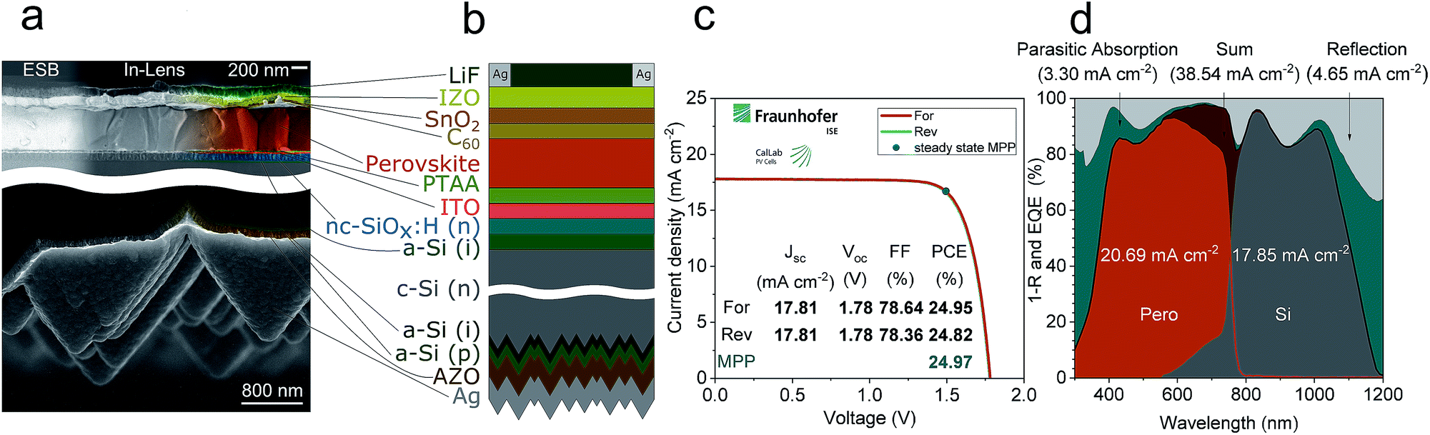 | ||
| Fig. 1 (a) Colored cross sectional SEM image of the top cell (upper panel) and back side of the bottom cell (lower panel) of a typical monolithic tandem solar cell used in this work. The left side of the top cell is recorded with an energy selective backscattered (ESB) detector, the right side with an in lens detector. Note that scale bars in the top and bottom panel are different as indicated; (b) schematic device layout of the tandem architecture utilized in this work. (c) Certified current density–voltage (J–V)-characteristics measured by Fraunhofer Institute for Solar Energy Systems (ISE) with the certified performance parameters as displayed in the inset table. Steady state efficiency from 400 second maximum power point (MPP)-tracking was 24.97%, see Fig. S3.† (d) Measured external quantum efficiency and reflection spectra of the certified tandem solar cell with integrated current densities and their sum as indicated. Additionally, the loss in current density due to parasitic absorption (as the difference between sum of the EQE and 1-reflectance) and reflection are shown. | ||
To ensure a high FF, the top TCO needs to be highly conductive. At the same time, the near infrared absorption needs to be mitigated, so that the light can be absorbed in the bottom cell. Adding 0.2%vol oxygen during the sputter process of IZO results in a good balance between transparency, conductivity and the optical band gap and is therefore used in our optimized process. More details can be found in ESI note 1.†
The resulting tandem device, containing a 20 nm thick n-type nc-SiOx:H and SnO2 processed at 100 °C deposition temperature, was sent for independent certification to CalLab, Fraunhofer Institute for Solar Energy Systems (ISE). Fig. 1c displays the J–V characteristics reported by the certification lab; a PCE of 25.0% was measured, stable during 400 seconds of maximum power point tracking (see Fig. S3†). The device exhibits virtually no hysteresis and the deviation between the maximum power point parameters obtained from MPP tracking and those from J–V measurement is negligible. The VOC of 1.78 V is close to the cumulative sub-cell VOCs as expected from single junction devices and to the VOCs found recently with similar device architectures.4,6,7 A FF of 78.6% is one of the highest measured for a perovskite/silicon tandem solar cell and will be discussed in more detail below. On the other hand, a JSC of 17.81 mA cm−2 indicates one of the limiting factors of the certified tandem solar cell. This is further confirmed by the EQE measurements, presented in Fig. 1d along with the total reflectance of the device presented as 1-R. The photocurrent densities are JPero = 20.69 mA cm−2 and JSi = 17.85 mA cm−2 for the perovskite top and silicon bottom cell, respectively. This shows that the certified tandem device is strongly current-mismatched with the silicon sub-cell being the limiting one. Although the JSC of a tandem solar cell can be higher than the minimum JSC of the sub-cells,41,42 for state of the art solar cells the tandem JSC is expected to be very close to the minimum JSC of the sub-cells (limiting sub-cell). This is valid when the limiting sub-cell (here: silicon) has a high shunt resistance. Assuming this, the integrated current density JSi of 17.85 mA cm−2 measured in-house is in very good agreement with the certified JSC of 17.81 mA cm−2 measured at Fraunhofer ISE. The mismatch m between JPero and JSi is more than 2.8 mA cm−2, which needs to be reduced in order to achieve higher PCEs. Fig. 1d displays the sum of the EQEs (black line) and the parasitic losses as the blue area between the sum and 1-R. The parasitic losses are high in the UV and near infrared (NIR) wavelength range and are below 1% on average between 550 nm and 1000 nm. The integrated reflection losses amount to an equivalent photocurrent of 4.65 mA cm−2 in the complete wavelength regime; between 750 nm and 1050 nm, there are distinct reflection features with 1.9 mA cm−2 reflection losses only in this region. In order to extract parasitic losses for each individual layer, an optical simulation was carried out using GenPro4 (Fig. S4†).43 We find, that in the UV region, mostly IZO, SnO2 and C60 absorb light, whereas in the infrared region the photons are absorbed by the IZO at the front side, by the ITO connecting the sub-cells and by the aluminum doped zinc oxide (AZO) and silver (Ag) at the backside of the cell. The rather high reflection losses and the strong current mismatch indicate that further optical optimizations are required.
In order to further improve the tandem solar cell, a lower temperature of the ALD SnO2 process was first considered. Exposing the perovskite for 1 h to 100 °C (in addition to the perovskite annealing) might reduce the perovskite top cell performance, thus limiting the tandem efficiency.44,45 Therefore, we analyze the SnO2 layer in terms of optical properties as a function of deposition temperature. Fig. 2a shows that changing the deposition temperature has an effect on the optical properties of the deposited layer, as evidenced by the shift in extinction coefficient and refractive index. At higher temperatures, a higher absorption in the UV is measured and the absorption onset becomes steeper. Simultaneously, the refractive index increases. However, using optical simulations including the measured differences in optical data, we find that changing the deposition temperature in the range of 80 °C to 200 °C does not have a major effect on JPero and JSi in our tandem device (Fig. S5a†). For higher deposition temperatures, the EQE of the perovskite improves for wavelengths above 370 nm but also reduces below 370 nm as the absorption of the SnO2 increases in that wavelength range. Overall, the cumulated current density JPero+Si is constant in the practically relevant range of 80 °C to 120 °C (Fig. S5b†). More importantly, changing the deposition temperature can have a strong effect on the electrical performance. Therefore, semitransparent perovskite solar cells with SnO2 deposited at moderate temperatures of 80 °C, 100 °C and 120 °C are fabricated and analyzed. The results, depicted in Fig. 2b and c, indeed show a beneficial effect on the FF by reducing the temperature from 120 °C to 80 °C, which directly transfers to the change in PCE. The VOC and JSC, however, are hardly affected by the different deposition temperatures of the ALD SnO2 (see Fig. S6a and b†).
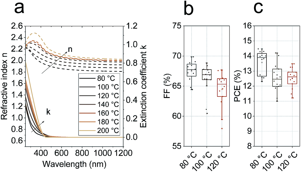 | ||
| Fig. 2 (a) Optical properties of SnO2 deposited via ALD at temperatures from 80 °C to 200 °C. The refractive index (n, left axis) and extinction coefficient (k, right axis) are extracted from spectroscopic ellipsometry measurements using Tauc–Lorentz oscillators. (b and c) FF and PCE for semitransparent perovskite solar cells with ALD SnO2 deposited at 80 °C, 100 °C and 120 °C. The cells have the same architecture as the tandem cell without a LiF anti-reflective coating and are illuminated through the IZO side. The corresponding VOC and JSC values are shown in ESI Fig. S6.† | ||
Additionally, the thickness of the top TCO in the tandem stack, here IZO, has a significant influence on parasitic absorption throughout the entire wavelength range. To analyze the impact of top electrode thickness, an optical simulation of the tandem stack with thicknesses of IZO between 60 nm and 130 nm in 10 nm steps is performed. Fig. S7† shows the simulated gain in current density, which amounts to ∼0.32 mA cm−2 when reducing the thickness from 130 nm to 90 nm. Further reducing the IZO thickness would be ideal to increase JPero and JSi. However, reducing the thickness also leads to a higher sheet resistance and might have a negative impact on the cell performance, especially reduction of FF. Therefore, 90 nm was used in the optimized device.
Apart from being the electron-selective contact layer for the bottom SHJ solar cell the use of n-type nc-SiOx:H between the perovskite and silicon absorber has two benefits: first, the refractive index at 633 nm of around 2.7 is in between those of the neighboring layers, which reduces reflection; second, this reflection can be spectrally tuned when the layer thickness is adapted for destructive interference in a particular wavelength range. For the n-type nc-SiOx:H, a thickness of around 95 nm was found both in simulations and experimental results to be ideal for monolithic perovskite/silicon tandem solar cells.15,29 Thus, this thickness is implemented in the further development.
Finally, the thickness of the perovskite absorber is fine-tuned by adjusting the spin coating speed to enable conditions closer to current matching.4,7 Fig. S8† presents optical simulations with varying perovskite thickness between 390 nm and 520 nm. While JPero+Si hardly changes, a thinner perovskite absorber layer will transmit more light into the silicon bottom cell, enhancing the JSi. As the sub-cell with the lower current approximately determines the JSC of the tandem cell, a maximum tandem JSC is expected for a perovskite thickness of around 470 nm for our design.
All above described optimizations are implemented into tandem solar cell devices and the results are shown in Fig. 3. Indeed, the optical losses are reduced and the sub-cells enable short circuit current densities closer to current matching. The JSC improved by 1.4 mA cm−2 to a value of 19.22 mA cm−2. The VOC remained almost unchanged (1.77 V) while the FF is slightly lower (76.6%). Overall, a stabilized PCE of 26.0% is achieved, confirmed by a 5 minute MPP-track as shown in Fig. 3a. Fig. 3b highlights the EQE spectra together with total reflectance depicted as 1-R for the optimized tandem design. Due to improved optics, interference patterns in the 800 nm to 1050 nm wavelength range are smoothened, reducing reflection by more than 1 mA cm−2 and increasing JSi. Compared to the device shown in Fig. 1c and d, the improved device is much closer to current matching, with only 0.9 mA cm−2 mismatch. In Fig. S9,† EQE spectra of similarly fabricated single junction silicon and perovskite cells are shown.
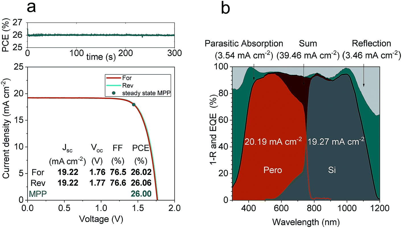 | ||
| Fig. 3 (a) J–V-characteristics of the optimized tandem solar cell with the performance metrics and a 5 min. MPP-track. (b) External quantum efficiency (EQE) and 1-reflectance (1-R) spectra of the same device. The integrated current densities are 20.19 mA cm−2 and 19.27 mA cm−2 for the perovskite and silicon cell sub-cells, respectively. Additionally, the integrated loss currents from parasitic absorption and 1-R are shown. | ||
To test the stability of these optimized tandem devices, a similar tandem solar cell with comparable performance as shown in Fig. 3 was glass/glass encapsulated with edge-sealant and stored in ambient conditions. Due to different optics after encapsulation, the PCE dropped from 26.0% to 24.6% mostly because of additional reflection from the air/glass interface, as compared to air/LiF. During 1000 h, the device was stored in ambient air and light conditions (i.e. 19–21 °C and 50–90% RH) and regularly MPP-tracked for at least 30 min at each data point. The measurements were performed at 25 °C, ambient humidity and under simulated full 1 sun AM1.5G illumination. The exact spectrum is shown later in Fig. 4a. The PCE as function of time is presented in Fig. S10† and found to be remarkably stable with a relative PCE drop of less than 1% for the last measurement after 1000 h of ambient storage.
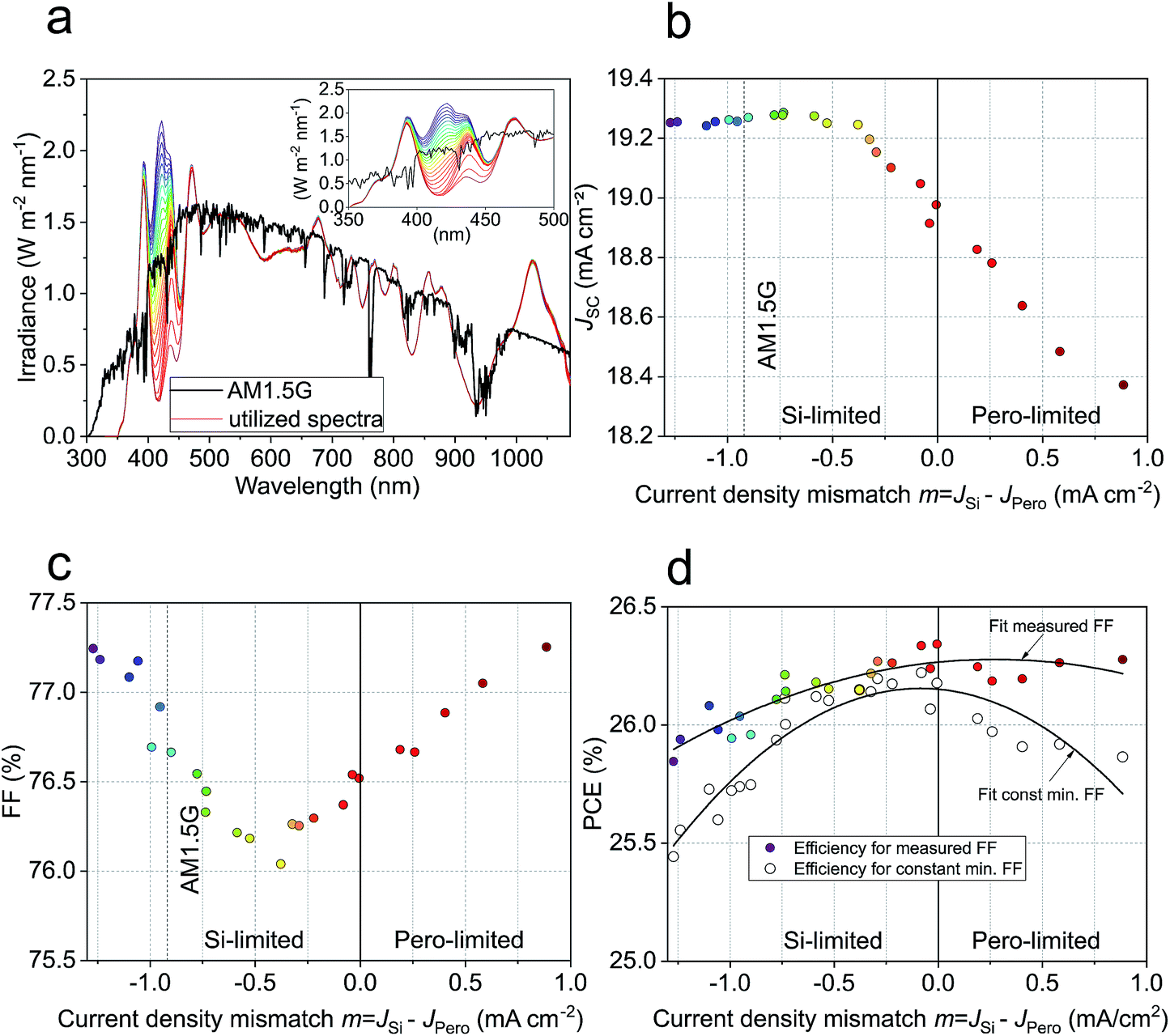 | ||
| Fig. 4 (a) Utilized spectra of the LED-based sun simulator. The illumination intensities of two selected LEDs emitting in the blue part of the spectrum are adjusted in order to get a spectrum with a higher or lower intensity in the blue wavelength range, as compared to the AM1.5G. (b–d) Short circuit current density, fill factor and PCE of the tandem solar cell from Fig. 4 as a function of the mismatch in calculated photogeneration currents between the sub-cells. Additionally, the power density is shown when assuming that the FF = FFmin and does not change with changing mismatch. | ||
As the optimized tandem device in Fig. 3 still shows current mismatch and the JPero+Si stays below 40 mA cm−2, the optical benefit of further reducing the front IZO thickness is tested. As described above, Fig. S7† shows simulation results for thinner front IZO. A JPero+Si above 40 mA cm−2 is only realized with IZO thicknesses of around 60 nm. Consequently, a tandem solar cell with this thin IZO layer is fabricated and the experimental results are presented in Fig. S11.† Integrated current densities from the EQE spectra up to 20.27 mA cm−2 for the top and 19.77 mA cm−2 for the bottom cell are measured, which indeed results in a JPero+Si of more than 40 mA cm−2. This current density is comparable to values reported by Sahli et al.4 for a fully textured tandem cell but is still lower than the best JSC of silicon single junction cells (42.87 mA cm−2).1 If the JPero+Si would be equally distributed between JPero and JSi, the tandem cell with thin IZO would exceed a JSC of 20 mA cm−2, a remarkable result for a planar front side tandem design. Due to a lower FF, which is mainly a result of lower shunt resistance and slightly higher series resistance – the latter due to higher ohmic losses in thinner IZO – the stabilized PCE during MPP-tracking is only 25.3% (see Fig. S11†). For the optimal performance with thin IZO, metal fingers are necessary and to optimize the resistive versus shading losses, opto-electrical simulations are required,46 which is a subject of future work.
Comparing the two tandem solar cells, presented in Fig. 1 and 3, we observe a lower FF for the device that operates closer to current matching. Besides the possibility of a cell-to-cell variation, operating the sub-cells under strong non-matching conditions should improve the tandem FF, as reported for other tandem technologies.18,30,33 As a thorough understanding of the influence of non-current matching conditions is important for (a) device understanding and (b) energy yield analysis, the FF of the best performing tandem solar cell shown in Fig. 3 is measured here for various illumination spectra, leading to non-matching conditions. Using a LED-based sun simulator, the intensity of individual LEDs can be adjusted while leaving the others unchanged. Thus, the device can be measured under different non-matching conditions m. As basis, the simulated AM1.5G spectrum is used. To increase or decrease the irradiance in the blue region, the intensities of two blue LEDs (emission peaks centered at 420 nm and 440 nm) are changed, while leaving all other LEDs constant to simulate the AM1.5G spectrum. This way, only the current generation in the perovskite top cell is affected. Fig. 4a shows the utilized spectra including the AM1.5G reference spectrum. The measurement series starts with the highest intensity of blue light well above the blue intensity in the AM1.5G spectrum. Then the intensities of the two blue LEDs are decreased and a tandem J–V-curve for each spectrum is measured. The raw data of the 26 measurements are presented in Fig. S12,† plotted against the spectrum (measurement) number. The first and last J–V curve in the series are measured under AM1.5G illumination and ensure that there is no degradation of the cell and no drift of the spectrum during the course of the series. As the intensity of the blue light (i.e. current generation in the perovskite) decreases, the hysteresis of the tandem cell starts increasing, revealing that the hysteresis of the perovskite sub-cell is influenced by current mismatch. Interestingly, the hysteresis is decreased after the series is done. However, in the following, only the VOC to JSC (reverse scan) measurements will be considered. The currents of the sub-cells are calculated by integrating the sub-cell EQE multiplied by the measured spectra. From these, the mismatch m = JSi − JPero is calculated as the difference between JSi and JPero. Fig. 4b–d show the tandem JSC, FF and PCE as a function of mismatch. Due to the logarithmic dependence on JSC, the VOC is only marginally affected by the changing spectrum (Fig. S12†). As can be seen from the comparison of Fig. 4a and b, a stronger photogeneration in the blue wavelength range, i.e. a higher JPero, does not affect the tandem JSC, as this metric is limited by the unchanged bottom cell current. This confirms that the silicon sub-cell is limiting for the AM1.5G illumination conditions (see Fig. 4b) and high intensities of blue light, as seen in the EQE measurement shown in Fig. 3b. Once the blue intensity is lower than in the AM1.5G spectrum, the tandem cell becomes top cell limited, where the JSC is reduced in accordance to the reduced intensity (see positive current density mismatch values m = JSi − JPero in Fig. 4b).
Changing the spectrum and therefore changing the mismatch does not only have an effect on the current density, but also on the FF (Fig. 4c). It is typically reported that the FF is lowest when the tandem solar cell is operated close to the current matching point,30,33,47 but this is not necessarily exactly at the matching point and depends on the individual performance of the sub-cells.31 Interestingly, the FF minimum occurs here when the silicon bottom cell is the limiting sub-cell. With a slope of −1.31% FF per mA cm−2 mismatch, a FF of 79% is expected for a mismatch of −2.8 mA cm−2, which is the mismatch value of the certified tandem cell discussed above. As this mismatch-predicted FF value is close to the FF of the certified cell, it strongly supports the assumption that the reduced FF after decreasing the photocurrent mismatch is mainly due to the device physics instead of a cell-to-cell variation. The benefit of ALD optimization and enhanced resistive losses from thinner front IZO counterbalance here. Although, the FF can change with the photocurrent due to e.g. reduced collection losses, we can exclude this effect to be dominant in our tandem solar cell as the FF of a similar fabricated cell does not vary with JSC in the relevant photocurrent range utilized for mismatch analysis.6
Fig. 4d shows the PCE of the tandem solar cell as a function of the current density mismatch. The intensity of each spectrum is calculated as stated in ESI note 3.† Although the JSC decreases for a mismatch m > −0.3 mA cm−2, the PCE increases due to the increasing FF (colored data points). The quadratic fit of the PCE calculated with the measured FF reveals a maximum PCE of 26.3% close to current matching. Furthermore, the PCE is calculated assuming the measured JSC and VOC, but a constant FF = FFmin with FFmin being the minimum FF measured in the series (white data points). The comparison between the constant and non-constant FF highlights that the changing FF mostly compensates the drop in JSC, thus leading to a broader peak around the maximum PCE. For a mismatch of m = 1 mA cm−2, the PCE-difference between both curves is 0.49% while for m = −1 mA cm−2 the PCEs differ by 0.26%. The PCE of a slightly mismatched monolithic tandem solar cells suffers only marginally from the decreased JSC. This is highly important for energy yield analysis, especially when comparing monolithic 2-terminal with 4-terminal tandem solar cells. One of the arguments in favor of 4-terminal devices is to avoid decrease in performance due to current reduction if current mismatch occurs. However, we show that in 2-terminal, monolithic devices the FF increases with mismatch (see colored data points in Fig. 4c). Thus, the drop in JSC is mostly compensated, leading to a PCE which is less sensitive to current density mismatch. Assuming an ideal current redistribution with JSC,matched = 0.5JPero+Si = 19.73 mA cm−2 for both sub-cells in Fig. 3b, using the measured values for FFmatched, and VOC,matched extracted for m = 0, a PCE of 26.6% would be reached.
To validate the experimental results in Fig. 4c, we perform electrical simulations using the electronic design automation software LTspice (for more details and parameters see ESI note 4†).48 An equivalent circuit diagram consisting of two series connected single diode models was built as shown in Fig. S14a.† In the first step, we prove that the FF minimum is not necessarily at the current matching point for any kind of monolithic tandem solar cell. For this, two identical solar cells are connected in series in this simulation. When sweeping the JTop and JBottom while maintaining a constant JTop+Bottom, the FF indeed changes as a function of current mismatch (see Fig. S14b,† upper graph) with a FF minimum for current matching conditions. The same procedure is carried out for a reduced shunt resistance RSh of either the top or the bottom cell. Now, the FF minimum is not in the current matching point anymore but shifts to the bottom cell limited side for a low RSh,Bottom and to the top cell limited side for a low RSh,Top (Fig. S14b†). Although the experimentally detected FF minimum is present for silicon limiting illumination conditions (Fig. 4c), we do not expect to have a lower RSh in the silicon bottom cell compared to the perovskite top cell. The difference between the simulation and experiment is discussed below. The bottom graph in Fig. S14b† shows that a mismatch between JPero and JSi might be necessary for achieving the highest PCE. As stated earlier in this paper, the highest power is achieved if both sub-cells have the same JMPP. The necessity of current matching depends on the shunt resistance and with that overall of the individual sub-cells (i.e. the difference between JSC and JMPP). If the difference between JSC and JMPP of both sub-cells is similar, JSC-matching leads to the highest power output. If the difference between JSC and JMPP is unequal for both sub-cells, a JSC-mismatch is needed to achieve JMPP-matching and with that, the highest power output. In a second step, we attempt to reconstruct the measured tandem J–V-characteristics using electrical simulations. For this, single junction silicon and perovskite (opaque) cells are fabricated with similar device layout as in our tandem solar cell and parametrized using a single diode model. Fig. S15a and b† show the measured J–Vs at different intensities of the single junction solar cells as well as the simulated J–Vs. We use the parameters of the fitted single junction cells to reconstruct the tandem solar cell and simulate the experiment. Solely the series resistance Rs and saturation current of the perovskite J0,Pero are adjusted slightly to match the tandem conditions (see ESI note 4†). The simulated JSC and FF as a function of mismatch m are shown in Fig. S15c and d† and reveal a higher and shifted FF minimum but a similar variation of JSC. Using the FF, VOC and JSC from simulated results would lead to a PCE of 27.6% for AM1.5G illumination for the tandem device presented in see Fig. 3, mostly due to higher FF in simulation. Comparing the J–Vs with most negative and most positive mismatch, the difference between the simulated and experimentally measured J–Vs appears to be just around the MPP (Fig. S15e†). For unmatched sub-cells, charge carriers accumulate at the recombination contact. This could affect the recombination behavior. Moreover, the electric fields and with this, the charge collection of the sub-cells is affected by the charge accumulation. This might also be the reason for the dependency of the hysteresis on the mismatch. Additionally, the recombination layer might behave non-ohmic, thus another electrical component needs to be implemented in the simulation. Further investigation is needed to understand the device physics in more detail, to exactly reconstruct the monolithic tandem solar cell in an electrical simulation and with this, increase the PCE. If we assume an ideal contact design in the tandem solar cell for example by implementing grid fingers, leading to a series resistance of RS = 0 Ω cm2 (for this, we additionally assume a negligible series resistance of the bulk and vanishing contact resistance), the simulated tandem device could reach a PCE of 29% (Fig. S16b†). Here the JPero+Si is maintained constant at 39.46 mA cm−2, the same JPero+Si as for the device shown in Fig. 3. Furthermore, we simulate a monolithic tandem solar cell by using electrical parameters from record p–i–n perovskite49 and both side contacted c-Si cells.34,50 By neglecting the series resistance, which mostly stems from the perovskite sub-cell, the FF increases and therefore a maximum PCE of 31.0% is expected due to improved VOC (Fig. S14d†).
Conclusions
In summary, we implemented a transparent n-type top contact layer stack in monolithic silicon/perovskite tandem solar cells in order to achieve a certified PCE of 25.0% at highly unmatched photocurrents. Further improvements of the rear junction silicon bottom cell with adjusted n-type nc-SiOx:H layer thickness, the n-type top cell contact with proper ALD SnO2 deposition temperature and IZO thickness, as well as adjusted perovskite thickness led to a remarkable tandem PCE of 26.0%. Further reducing the front IZO thickness allowed JSCs over 19.7 mA cm−2 and cumulative current densities JPero+Si over 40 mA cm−2 in tandem cells with a planar front side. As the FF was found to depend on the mismatch condition m = JSi − JPero, the sub-cell mismatch for the best tandem device was analyzed by varying the illumination spectrum. We show that the FF improves under unmatched current conditions of the tandem solar cell and that the loss in tandem PCE due to lower JSC at unmatched conditions is less pronounced than it would be with a constant FF. This dependence is highly important for energy yield analysis, especially when comparing 2-terminal and 4-terminal tandem solar cells. Electrical simulations based on input parameters from reference single junction devices parametrized with a single diode model confirmed the increasing FF for unmatched monolithic tandem solar cells. The simulation of the tandem performance shows that the FF in our experimentally realized device is lower than the FF expected from simulations, leaving room for improvement. An ideal series resistance can lead to a PCE of 29% for our tandem architecture. The simulation of a monolithic tandem solar cell with record perovskite and silicon cells from literature and a negligible series resistance reveals a PCE of 31%. Therefore, our work provides a detailed device understanding under different current matching conditions. This is mandatory to improve the PCE potential of silicon/perovskite tandem solar cells to predicted values above 30%.Materials and methods
Perovskite materials
Anhydrous DMSO (dimethyl sulfoxide), DMF (dimethylformamide), and toluene were purchased from Sigma Aldrich. PTAA (poly [bis(4-phenyl)(2,5,6-trimentlyphenyl)amine]), C60 (purity = 99.9%) and lithium fluoride (purity ≥ 99.99%) were purchased from Sigma Aldrich. FAI (formamidinium iodide) and MABr (methylammonium bromide) were purchased from Dyenamo. PbI2 and PbBr2 were bought from TCI. CsI was purchased from abcr GmbH. The ceramic 2 inch IZO target was purchased from FHR Anlagenbau GmbH.Perovskite solar cell preparation on silicon bottom cell
The fabricated perovskite sub-cell has an inverted (p–i–n) planar structure and a layer configuration of Si bottom cell (incl. ITO)/PTAA/perovskite/C60/SnO2/IZO, where IZO is zinc doped indium oxide. The silicon substrates were blown with nitrogen before use. All the spin-coating layer deposition steps were conducted in a nitrogen atmosphere. The hole transport material PTAA (2mg ml−1 in toluene) was deposited using spin-coating (4000 rpm for 30 s) and annealed for 10 min at 100 °C, leading to a 10 nm to 15 nm thick layer. The perovskite was prepared following the typical triple cation process.38,51 In short, 1.5 M nominal PbI2 and PbBr2 in DMF![[thin space (1/6-em)]](https://www.rsc.org/images/entities/char_2009.gif) :DMSO = 4:1 volume were first prepared as stock solutions and then added to FAI and MABr with 10% PbX2 excess, respectively (X = I or Br). The so obtained FAPbI3 and MAPbBr3 were then mixed in 5:1 volume ratio to obtain the “double cation” perovskite. Finally, 5% volume of 1.5 M nominal CsI in DMSO was added to form the “triple cation” perovskite. 120 μl of perovskite solution was then spread on the substrate and spun using one step spin-coating process (4000 rpm or 5000 rpm for 35 s). 25 s after the start of a spinning, 500 μl ethyl acetate anti-solvent drop was utilized. The films were annealed at 100 °C for 1 h. The perovskite thickness is around 580 nm and 460 nm for 4000 rpm and 5000 rpm. Afterwards, 15 nm C60 was thermally evaporated at a rate of 0.15 Å s−1 at 400 °C. 20 nm SnO2 were prepared by thermal ALD in an Arradiance GEMStar reactor. Tetrakis(dimethylamino)tin(IV) (TDMASn) was used as the Sn precursor and was held at 60 °C in a stainless steel container. Water was used as oxidant, and was delivered from a stainless steel container without intentional heating, whereas the precursor delivery manifold was heated to 115 °C. For the deposition at 100 °C, the TDMASn/purge1/H2O/purge2 times are 1 s/7.5 s/0.2 s/10 s with corresponding nitrogen flows of 30 sccm/90 sccm/90 sccm/90 sccm. With this, 167 cycles leads to 20 nm tin oxide. For the deposition at the lower temperature of 80 °C, the purging times were slightly increased (i.e. times of 1 s/10 s/0.2 s/15 s) to account for less efficient purging of reactants and their reaction products at lower temperatures. 140 cycles were needed to deposit 20 nm at 80 °C. IZO was sputtered in a Roth&Rau MicroSys 200 PVD. The 2 inch ceramic target consisted of 90%wt. In2O3 and 10%wt. ZnO. At a RF-power of 70 W, the cells oscillated under the target to have a uniform deposition. To add additional oxygen to the deposition chamber, a mix of Ar and O2 is added. The added amount of oxygen ranges from 0.0%vol to 0.25%vol while the total gas flow is the same for all depositions. A 150 nm thick Ag metal frame was evaporated through a shadow mask as a top contact. Finally, 100 nm LiF was evaporated to serve as an anti-reflective coating.
:DMSO = 4:1 volume were first prepared as stock solutions and then added to FAI and MABr with 10% PbX2 excess, respectively (X = I or Br). The so obtained FAPbI3 and MAPbBr3 were then mixed in 5:1 volume ratio to obtain the “double cation” perovskite. Finally, 5% volume of 1.5 M nominal CsI in DMSO was added to form the “triple cation” perovskite. 120 μl of perovskite solution was then spread on the substrate and spun using one step spin-coating process (4000 rpm or 5000 rpm for 35 s). 25 s after the start of a spinning, 500 μl ethyl acetate anti-solvent drop was utilized. The films were annealed at 100 °C for 1 h. The perovskite thickness is around 580 nm and 460 nm for 4000 rpm and 5000 rpm. Afterwards, 15 nm C60 was thermally evaporated at a rate of 0.15 Å s−1 at 400 °C. 20 nm SnO2 were prepared by thermal ALD in an Arradiance GEMStar reactor. Tetrakis(dimethylamino)tin(IV) (TDMASn) was used as the Sn precursor and was held at 60 °C in a stainless steel container. Water was used as oxidant, and was delivered from a stainless steel container without intentional heating, whereas the precursor delivery manifold was heated to 115 °C. For the deposition at 100 °C, the TDMASn/purge1/H2O/purge2 times are 1 s/7.5 s/0.2 s/10 s with corresponding nitrogen flows of 30 sccm/90 sccm/90 sccm/90 sccm. With this, 167 cycles leads to 20 nm tin oxide. For the deposition at the lower temperature of 80 °C, the purging times were slightly increased (i.e. times of 1 s/10 s/0.2 s/15 s) to account for less efficient purging of reactants and their reaction products at lower temperatures. 140 cycles were needed to deposit 20 nm at 80 °C. IZO was sputtered in a Roth&Rau MicroSys 200 PVD. The 2 inch ceramic target consisted of 90%wt. In2O3 and 10%wt. ZnO. At a RF-power of 70 W, the cells oscillated under the target to have a uniform deposition. To add additional oxygen to the deposition chamber, a mix of Ar and O2 is added. The added amount of oxygen ranges from 0.0%vol to 0.25%vol while the total gas flow is the same for all depositions. A 150 nm thick Ag metal frame was evaporated through a shadow mask as a top contact. Finally, 100 nm LiF was evaporated to serve as an anti-reflective coating.
Silicon solar cell preparation
The silicon heterojunction (SHJ)-bottom cell was fabricated on a 260 μm thick polished FZ 〈100〉 n-type crystalline silicon (c-Si) wafer in a rear junction configuration. The front surface of the wafer was left polished in order to facilitate the perovskite top cell deposition, while the rear surface of the wafer was wet-chemically textured to obtain random pyramid with 〈111〉 facets in order to improve the optical response of the bottom cell in the NIR region. After a final RCA clean and a 3 minute HF dip (1% dilution in water) to strip the SiO2 of the surface, a 5 nm thick, intrinsic (i) amorphous silicon (a-Si:H) layer was grown on both sides of the c-Si wafer in order to passivate the c-Si surface. On the textured back-side, a 5 nm thick, p-doped a-Si:H was deposited on the rear passivating layer to form the junction of the SHJ cell. On the polished front-side, a 20 nm thick, n-doped nanocrystalline silicon oxide layer (nc-SiOx:H) with a refractive index, n, of 2.7 at 633 nm was used as a front surface field (FSF) of the SHJ bottom cell and intermediate layer between the top and the bottom cells. For the second optimization, this thickness was increased to 95 nm. All the a- and nc-Si layers were deposited with an Applied Materials (AKT1600) plasma enhanced chemical vapor deposition (PECVD) tool. In order to contact the bottom cell a ZnO:Al/Ag layer stack was deposited on the textured back-side and a 20 nm thick ITO layer was deposited on the polished front-side on top of the nc-SiOx:H interlayer, both depositions were DC-sputtered in an in-line sputtering tool from Leybold Optics. The contact layers of the silicon were deposited using shadow masks with an opening of 1 × 1 cm2.Silicon single junction solar cell preparation
To fabricate a silicon single junction, 80 nm IZO is additionally deposited on the 20 nm ITO of the bottom cell in order to reduce the sheet resistance. As for the tandem solar cell, a metal frame is evaporated as a top contact.Semitransparent perovskite single junction solar cell preparation
The semitransparent solar cells are manufactured as described in the section of the perovskite solar cell preparation on silicon bottom cells. Instead of the silicon bottom cell, an ITO coated glass substrate (25 × 25 mm, 15 Ω sq−1, patterned by Automatic Research GmbH) was used and cleaned sequentially for 15 min with Acetone, Mucasol (2%vol in water), DI-water and isopropanol in an ultrasonic bath. Before the deposition of the HTM, the samples were treated in an UV-ozone cleaner for 15 min.Tin oxide layers for optical characterization
For optical characterization, tin oxide was deposited on a silicon wafer coated with 450 nm silicon oxide. For the deposition temperature of 80 °C, the parameters are mentioned in the section “perovskite solar cell fabrication”. For all other temperatures, the pulse- and purge times and nitrogen flows are equal to the deposition of tin oxide at 100 °C.Device characterization
The current density–voltage (J–V) measurements were performed under standard test conditions (25 °C, LED based sun simulator from Wavelabs, class AAA), adjusted with a non-filtered calibrated silicon reference cell (Fraunhofer ISE). The scan rate was 0.25 V s−1 with a voltage increment of 20 mV. The external quantum efficiency (EQE) was measured as a function of wavelength from 300 nm to 1200 nm with a step of 10 nm using a home built small spot EQE system. The beam size is 2 × 5 mm2, thus smaller than the active area. When measuring perovskite top cell, infrared (850 nm) bias light was applied along with 0.6 V bias voltage to ensure a measurement in short circuit conditions. Additionally, the cell is slightly illuminated with blue (455 nm) light that partially increases the signal to noise ratio. When measuring silicon bottom cell, blue (455 nm) bias light was applied. The EQE of the silicon bottom cell is not affected by bias voltage, as the shunt resistance of the silicon cell is very high. Reflection was measured as a function of wavelength from 300 nm to 1200 nm with a step of 5 nm using an integrating sphere with a PerkinElmer Lambda – 1050 UV/VIS/NIR spectrophotometer, calibrated with a white Spectralon. The optical properties of ALD SnO2 were evaluated by spectroscopic ellipsometry. Measurements were performed using a Sentech SE 850 at angles of incidence 50°, 60° and 70°. The dielectric function was modeled using Tauc–Lorentz oscillators to account for the absorption for energies above the band gap.Author contributions
E. K., M. J., P. T., A. A. and Lu. K. developed and optimized the perovskite solar cell fabrication process. E. K. fabricated the tandem devices, performed the measurements and optimized the top contact. A. B. M. V., La. K. and B. S. developed and optimized the silicon-heterojunction solar cell fabrication process and fabricated bottom cells. B. M. and E. K. optimized the SnO2 process and performed and analyzed spectroscopic ellipsometry measurements. E. K., P. T. and A. A. performed the optical and electrical simulations. All authors participated in writing the manuscript and proofreading as well as correcting. B. R., R. S., B. S. and S. A. initiated and supervised the project.Conflicts of interest
There are no conflicts to declare.Acknowledgements
The authors acknowledge help in technical assistance by T. Lußky, H. Heinz, M. Gabernig, C. Klimm, C. Ferber, M. Muske, Institute for Silicon Photovoltaics and Tobias Henschel, Katja Mayer-Stillrich, Holger Rhein, PVcomB. The authors acknowledge funding from HyPerCells (Hybrid Perovskite Solar Cells, http://www.perovskites.de) joint Graduate School, as well as from the German Federal Ministry for Economic Affairs and Energy (BMWi) through the “PersiST” project (grant no. 0324037C). Further funding was provided by the Federal Ministry of Education and Research (BMBF) for funding of the Young Investigator Group Perovskite Tandem Solar Cells within the program “Materialforschung für die Energiewende” (grant no. 03SF0540) and by the Helmholtz Foundation within the HySPRINT Innovation lab project.References
- M. A. Green, Y. Hishikawa, E. D. Dunlop, D. H. Levi, J. Hohl-Ebinger and A. W. Y. Ho-Baillie, Prog. Photovoltaics, 2018, 26, 427–436 Search PubMed.
- K. Yoshikawa, H. Kawasaki, W. Yoshida, T. Irie, K. Konishi, K. Nakano, T. Uto, D. Adachi, M. Kanematsu, H. Uzu and K. Yamamoto, Nat. Energy, 2017, 2, 17032 CrossRef CAS.
- A. Richter, M. Hermle and S. W. Glunz, IEEE J. Photovolt., 2013, 3, 1184–1191 Search PubMed.
- F. Sahli, J. Werner, B. A. Kamino, M. Bräuninger, R. Monnard, B. Paviet-Salomon, L. Barraud, L. Ding, J. J. Diaz Leon, D. Sacchetto, G. Cattaneo, M. Despeisse, M. Boccard, S. Nicolay, Q. Jeangros, B. Niesen and C. Ballif, Nat. Mater., 2018, 17, 820–826 CrossRef CAS PubMed.
- B. Chen, Z. Yu, K. Liu, X. Zheng, Y. Liu, J. Shi, D. Spronk, P. N. Rudd, Z. Holman and J. Huang, Joule, 2018, 1–14 Search PubMed.
- M. Jošt, E. Köhnen, A. B. Morales-Vilches, B. Lipovšek, K. Jäger, B. Macco, A. Al-Ashouri, J. Krč, L. Korte, B. Rech, R. Schlatmann, M. Topič, B. Stannowski and S. Albrecht, Energy Environ. Sci., 2018, 11, 3511–3523 RSC.
- K. A. Bush, S. Manzoor, K. Frohna, Z. J. Yu, J. A. Raiford, A. F. Palmstrom, H.-P. Wang, R. Prasanna, S. F. Bent, Z. C. Holman and M. D. McGehee, ACS Energy Lett., 2018, 3, 2173–2180 CrossRef CAS.
- D. Zhao, Y. Yu, C. Wang, W. Liao, N. Shrestha, C. R. Grice, A. J. Cimaroli, L. Guan, R. J. Ellingson, K. Zhu, X. Zhao, R.-G. Xiong and Y. Yan, Nat. Energy, 2017, 2, 17018 CrossRef CAS.
- T. Leijtens, R. Prasanna, K. A. Bush, G. E. Eperon, J. A. Raiford, A. Gold-Parker, E. J. Wolf, S. A. Swifter, C. C. Boyd, H.-P. Wang, M. F. Toney, S. F. Bent and M. D. McGehee, Sustainable Energy Fuels, 2018, 2, 2450–2459 RSC.
- T. Todorov, T. Gershon, O. Gunawan, Y. S. Lee, C. Sturdevant, L. Y. Chang and S. Guha, Adv. Energy Mater., 2015, 5, 1–6 CrossRef.
- Q. Han, Y.-T. Hsieh, L. Meng, J.-L. Wu, P. Sun, E.-P. Yao, S.-Y. Chang, S.-H. Bae, T. Kato, V. Bermudez and Y. Yang, Science, 2018, 361, 904–908 CrossRef CAS PubMed.
- M. Jošt, T. Bertram, D. Koushik, J. A. Marquez, M. A. Verheijen, M. D. Heinemann, E. Köhnen, A. Al-Ashouri, S. Braunger, F. Lang, B. Rech, T. Unold, M. Creatore, I. Lauermann, C. A. Kaufmann, R. Schlatmann and S. Albrecht, ACS Energy Lett., 2019, 583–590 CrossRef.
- OxfordPV, Oxford PV perovskite solar cell achieves 28% efficiency, https://www.oxfordpv.com/news/oxford-pv-perovskite-solar-cell-achieves-28-efficiency, accessed 5 February 2019.
- K. Jäger, L. Korte, B. Rech and S. Albrecht, Opt. Express, 2017, 25, A473 CrossRef PubMed.
- L. Mazzarella, M. Werth, K. Jäger, M. Jošt, L. Korte, S. Albrecht, R. Schlatmann and B. Stannowski, Opt. Express, 2018, 26, A487 CrossRef CAS PubMed.
- M. H. Futscher and B. Ehrler, ACS Energy Lett., 2016, 1, 863–868 CrossRef CAS.
- T. Leijtens, K. A. Bush, R. Prasanna and M. D. McGehee, Nat. Energy, 2018, 3, 828–838 CrossRef CAS.
- M. T. Hörantner and H. J. Snaith, Energy Environ. Sci., 2017, 10, 1983–1993 RSC.
- B. Chen, X. Zheng, Y. Bai, N. P. Padture and J. Huang, Adv. Energy Mater., 2017, 7, 1602400 CrossRef.
- J. Werner, F. Sahli, F. Fu, J. J. Diaz Leon, A. Walter, B. A. Kamino, B. Niesen, S. Nicolay, Q. Jeangros and C. Ballif, ACS Energy Lett., 2018, 3, 2052–2058 CrossRef CAS.
- J. H. Heo, S. H. Im, J. H. Noh, T. N. Mandal, C.-S. Lim, J. A. Chang, Y. H. Lee, H. Kim, A. Sarkar, M. K. Nazeeruddin, M. Grätzel and S. Il Seok, Nat. Photonics, 2013, 7, 486–491 CrossRef CAS.
- W. S. Yang, B.-W. Park, E. H. Jung, N. J. Jeon, Y. C. Kim, D. U. Lee, S. S. Shin, J. Seo, E. K. Kim, J. H. Noh and S. Il Seok, Science, 2017, 356, 1376–1379 CrossRef CAS PubMed.
- W. S. Yang, J. H. Noh, N. J. Jeon, Y. C. Kim, S. Ryu, J. Seo and S. I. Seok, Science, 2015, 348, 1234–1237 CrossRef CAS PubMed.
- Q. Jiang, Z. Chu, P. Wang, X. Yang, H. Liu, Y. Wang, Z. Yin, J. Wu, X. Zhang and J. You, Adv. Mater., 2017, 1703852, 1–7 Search PubMed.
- H. Shen, S. T. Omelchenko, D. A. Jacobs, S. Yalamanchili, Y. Wan, D. Yan, P. Phang, T. Duong, Y. Wu, Y. Yin, C. Samundsett, J. Peng, N. Wu, T. P. White, G. G. Andersson, N. S. Lewis and K. R. Catchpole, Sci. Adv., 2018, 4, eaau9711 CrossRef PubMed.
- Y. Wu, D. Yan, J. Peng, T. Duong, Y. Wan, S. P. Phang, H. Shen, N. Wu, C. Barugkin, X. Fu, S. Surve, D. Grant, D. Walter, T. P. White, K. R. Catchpole and K. J. Weber, Energy Environ. Sci., 2017, 10, 2472–2479 RSC.
- S. Altazin, L. Stepanova, J. Werner, B. Niesen, C. Ballif and B. Ruhstaller, Opt. Express, 2018, 26, A579 CrossRef CAS PubMed.
- K. A. Bush, A. F. Palmstrom, Z. J. Yu, M. Boccard, R. Cheacharoen, J. P. Mailoa, D. P. McMeekin, R. L. Z. Hoye, C. D. Bailie, T. Leijtens, I. M. Peters, M. C. Minichetti, N. Rolston, R. Prasanna, S. Sofia, D. Harwood, W. Ma, F. Moghadam, H. J. Snaith, T. Buonassisi, Z. C. Holman, S. F. Bent and M. D. McGehee, Nat. Energy, 2017, 2, 1–7 Search PubMed.
- L. Mazzarella, Y.-H. Lin, S. Kirner, A. B. Morales-Vilches, L. Korte, S. Albrecht, E. Crossland, B. Stannowski, C. Case, H. J. Snaith and R. Schlatmann, Adv. Energy Mater., 2019, 1803241, 1803241 CrossRef.
- W. E. McMahon, K. E. Emery, D. J. Friedman, L. Ottoson, M. S. Young, J. S. Ward, C. M. Kramer, A. Duda and S. Kurtz, Prog. Photovoltaics, 2008, 16, 213–224 Search PubMed.
- M. Bonnet-Eymard, M. Boccard, G. Bugnon, F. Sculati-Meillaud, M. Despeisse and C. Ballif, Sol. Energy Mater. Sol. Cells, 2013, 117, 120–125 CrossRef CAS.
- M. Zeman, J. A. Willemen, L. L. A. Vosteen, G. Tao and J. W. Metselaar, Sol. Energy Mater. Sol. Cells, 1997, 46, 81–99 CrossRef CAS.
- C. Ulbrich, C. Zahren, A. Gerber, B. Blank, T. Merdzhanova, A. Gordijn and U. Rau, Int. J. Photoenergy, 2013, 2013, 1–7 CrossRef.
- A. Richter, J. Benick, F. Feldmann, A. Fell, M. Hermle and S. W. Glunz, Sol. Energy Mater. Sol. Cells, 2017, 173, 96–105 CrossRef CAS.
- A. Magomedov, A. Al-Ashouri, E. Kasparavičius, S. Strazdaite, G. Niaura, M. Jošt, T. Malinauskas, S. Albrecht and V. Getautis, Adv. Energy Mater., 2018, 8, 1801892 CrossRef.
- M. Stolterfoht, C. M. Wolff, Y. Amir, A. Paulke, L. Perdigón-Toro, P. Caprioglio and D. Neher, Energy Environ. Sci., 2017, 10, 1530–1539 RSC.
- M. Stolterfoht, C. M. Wolff, J. A. Márquez, S. Zhang, C. J. Hages, D. Rothhardt, S. Albrecht, P. L. Burn, P. Meredith, T. Unold and D. Neher, Nat. Energy, 2018, 3, 847–854 CrossRef CAS.
- M. Saliba, J.-P. Correa-Baena, C. M. Wolff, M. Stolterfoht, N. Phung, S. Albrecht, D. Neher and A. Abate, Chem. Mater., 2018, 30, 4193–4201 CrossRef CAS.
- K. O. Brinkmann, J. Zhao, N. Pourdavoud, T. Becker, T. Hu, S. Olthof, K. Meerholz, L. Hoffmann, T. Gahlmann, R. Heiderhoff, M. F. Oszajca, N. A. Luechinger, D. Rogalla, Y. Chen, B. Cheng and T. Riedl, Nat. Commun., 2017, 8, 1–9 CrossRef PubMed.
- L. Hoffmann, D. Theirich, D. Schlamm, T. Hasselmann, S. Pack, K. O. Brinkmann, D. Rogalla, S. Peters, A. Räupke, H. Gargouri and T. Riedl, J. Vac. Sci. Technol., A, 2018, 36, 01A112 CrossRef.
- J. Gilot, M. M. Wienk and R. A. J. Janssen, Adv. Mater., 2010, 22, E67–E71 CrossRef CAS PubMed.
- J. Gilot, M. M. Wienk and R. A. J. Janssen, Adv. Funct. Mater., 2010, 20, 3904–3911 CrossRef CAS.
- R. Santbergen, T. Meguro, T. Suezaki, G. Koizumi, K. Yamamoto and M. Zeman, IEEE J. Photovolt., 2017, 7, 919–926 Search PubMed.
- A. Dualeh, P. Gao, S. Il Seok, M. K. Nazeeruddin and M. Grätzel, Chem. Mater., 2014, 26, 6160–6164 CrossRef CAS.
- B. Conings, J. Drijkoningen, N. Gauquelin, A. Babayigit, J. D'Haen, L. D'Olieslaeger, A. Ethirajan, J. Verbeeck, J. Manca, E. Mosconi, F. De Angelis and H.-G. Boyen, Adv. Energy Mater., 2015, 5, 1500477 CrossRef.
- T. Fellmeth, F. Clement and D. Biro, IEEE J. Photovolt., 2014, 4, 504–513 Search PubMed.
- S. Reynolds and V. Smirnov, Energy Procedia, 2015, 84, 251–260 CrossRef CAS.
- Linear Technology, LTspice, https://www.analog.com/en/design-center/design-tools-and-calculators/ltspice-simulator.html.
- D. Luo, W. Yang, Z. Wang, A. Sadhanala, Q. Hu, R. Su, R. Shivanna, G. F. Trindade, J. F. Watts, Z. Xu, T. Liu, K. Chen, F. Ye, P. Wu, L. Zhao, J. Wu, Y. Tu, Y. Zhang, X. Yang, W. Zhang, R. H. Friend, Q. Gong, H. J. Snaith and R. Zhu, Science, 2018, 360, 1442–1446 CrossRef CAS PubMed.
- M. A. Green, Y. Hishikawa, E. D. Dunlop, D. H. Levi, J. Hohl-Ebinger and A. W. Y. Ho-Baillie, Prog. Photovoltaics, 2018, 26, 3–12 Search PubMed.
- M. Saliba, T. Matsui, J.-Y. Seo, K. Domanski, J.-P. Correa-Baena, M. K. Nazeeruddin, S. M. Zakeeruddin, W. Tress, A. Abate, A. Hagfeldt and M. Grätzel, Energy Environ. Sci., 2016, 9, 1989–1997 RSC.
Footnote |
| † Electronic supplementary information (ESI) available. See DOI: 10.1039/c9se00120d |
| This journal is © The Royal Society of Chemistry 2019 |