Solid-state p-type dye-sensitized solar cells: progress, potential applications and challenges
Received
27th November 2018
, Accepted 6th February 2019
First published on 6th February 2019
Abstract
The fabrication of solid-state p-type dye-sensitized solar cells (p-ssDSCs) using electron transport materials instead of the conventional I−/I3− redox couple in liquid devices can completely eliminate the liquid phase and enhance the photovoltage. The performance of p-ssDSCs has been improved by optimizing the dyes and electron-transport materials. Moreover, p-ssDSCs provide a possibility to fabricate solid-state tandem dye-sensitized solar cells and show promising application in dye-sensitized solar fuel devices as well. Herein, the development of p-ssDSCs has been overviewed, their potential applications have been discussed, and the challenges remaining in p-ssDSCs have been highlighted.
Introduction
The p-type dye-sensitized solar cell (p-DSC) was first reported in 1999 by Lindquist and co-workers,1 in which a porphyrin dye was used as a photosensitizer, nanoporous NiO acted as a large band gap p-type semiconductor to load the dye, and a liquid I−/I3− electrolyte was adopted as a redox mediator to undertake electron transport between the counter electrode and photocathode. Subsequently, p-DSCs have been attracting scientists' interest due to their potential applications in the preparation of tandem dye-sensitized solar cells2,3 in cooperation with conventional n-type DSCs (n-DSCs)4 as well as in the fabrication of dye-sensitized solar fuel devices (DSSFDs).5–9 However, the p-DSCs with NiO as a p-type semiconductor and the I−/I3− redox couple always suffer from low photovoltages due to small energy difference (ΔE) between the valence band (VB) of NiO and the redox potential of the I−/I3− redox couple.10 Some studies have been focused on the development of new p-type semiconductors with respect to NiO;11–13 however, NiO still provides a higher photocurrent and has more facile preparation process than other materials. Researchers have also tried to use other redox couples, such as tris(1,2-diaminoethane)cobalt(III)/(II)14 and tris(acetylacetonato)iron(III)/(II),15 with more negative reduction potentials than I−/I3− to enlarge the ΔE. This kind of strategy indeed can improve the photovoltage without scarifying the photocurrent of the p-DSCs. However, such redox couples are always sensitive to oxygen, which makes the solar cell fabrication process more complex. Also, the system still contains organic solvents, with a potential issue of electrolyte leaking from the device. On the basis of this background, we proposed a concept of solid-state p-type dye-sensitized solar cells (p-ssDSCs) in 2016![[thin space (1/6-em)]](https://www.rsc.org/images/entities/char_2009.gif) 16 in order to eliminate the liquid phase existing in the conventional p-DSCs as well as to improve the photovoltage of p-DSCs. Some follow-up work further proved the concept of the p-ssDSCs and made progress toward improving the efficiency of this kind of device from different angles.17–20 The p-ssDSCs also showed potential applications in DSSFDs and tandem solar cells. In this perspective, I give an overview of the basic concept and progress of p-ssDSC, discuss their potential applications, and point out the challenges still left to be overcome.
16 in order to eliminate the liquid phase existing in the conventional p-DSCs as well as to improve the photovoltage of p-DSCs. Some follow-up work further proved the concept of the p-ssDSCs and made progress toward improving the efficiency of this kind of device from different angles.17–20 The p-ssDSCs also showed potential applications in DSSFDs and tandem solar cells. In this perspective, I give an overview of the basic concept and progress of p-ssDSC, discuss their potential applications, and point out the challenges still left to be overcome.
Basic concept of p-ssDSCs
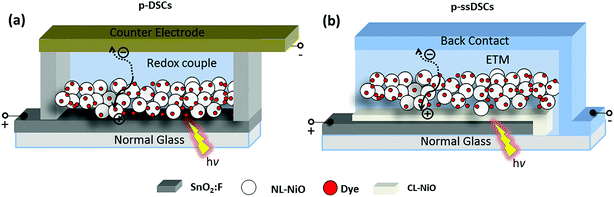
Fig. 1 shows the configurations of a conventional liquid p-DSC and a p-ssDSC. In a p-ssDSC, a solid-state electron-transport material (ETM) is used instead of the liquid electrolyte, such as I−/I3−, in a liquid device to undertake dye regeneration and electron transport between the dye-sensitized photocathode and back contact. The ETM should be able to infiltrate in the nanoporous p-type semiconductor (p-SC) film, such as NiO film, with a good contact with the dye. This requires that the ETM should have good solubility in the solvent for the solution-process or it may be in situ prepared in the p-SC film. In order to obtain a satisfactory photovoltage from a p-ssDSC, the ΔE between the VB of the p-SC and reduction potential of the ETM should be as large as possible, but the reduction potential of the ETM has to meet the need for dye regeneration. The ETM should also hold good electron mobility to efficiently transport electrons to the back contact.
 |
| | Fig. 1 Schematic of the configurations of a conventional liquid p-DSC (a) and a solid-state device p-ssDSC (b). | |
Proof of concept
In our proof-of-concept work for the p-ssDSCs,16 we chose [6,6]-phenyl-C61-butyric acid methyl ester (PCBM) as the ETM and a standard organic dye P121 as the photosensitizer (Fig. 2a) to fabricate our p-ssDSCs. PCBM is a benchmark organic ETM used in organic solar cells,22 showing electron mobility of ca. 2 × 10⁻³ cm2 V−1 s−1.23 It also has excellent thermal stability with a crystallization temperature and melting point of 195 °C and 290 °C, respectively.23 Its good solubility in many solvents makes it possible to fabricate solar cell by a low energy-consumption method, i.e., a solution process. Moreover, PCBM holds its first reduction potential at −0.4 V vs. a Normal Hydrogen Electrode (NHE), which is more negative than that of the I−/I3− redox couple, 0.3 V vs. NHE.16 The dye generation is also thermodynamically feasible, as the driving force for PCBM to regenerate P1 dye is 0.4 V. Theoretically, PCBM as the ETM in NiO-based p-ssDSCs should render a much higher photovoltage (VOC, 0.9 V) than that of the liquid device using the I−/I3− redox couple (0.2 V), as shown in Fig. 2b.
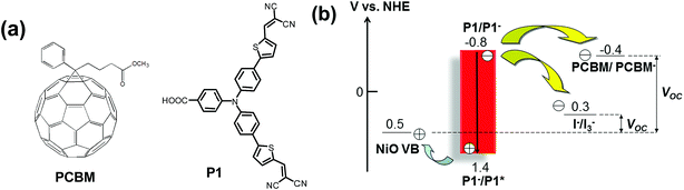 |
| | Fig. 2 The molecular structures of PCBM and P1 dye (a) and potential diagram of p-ssDSCs based on a PCBM ETM and liquid p-DSCs with the I−/I3− redox couple (b). | |
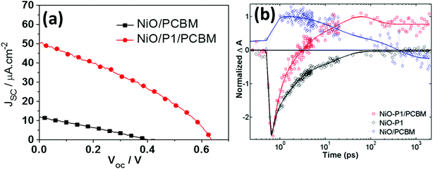
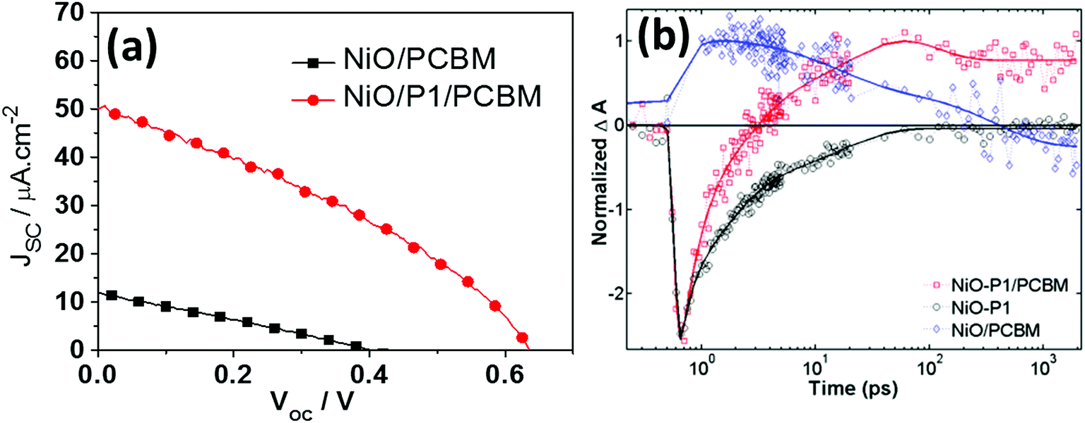
Different from liquid p-DSCs, in the p-ssDSCs, a compact NiO layer (see Fig. 1) should be placed between the FTO (SnO2:F) and nanoporous NiO layer, in order to block the physical contact between the FTO and the penetrated PCBM for suppressing the serious hole and electron recombination. With 100 nm Al as the back contact, a device based on NiO/P1/PCBM rendered a photocurrent density (JSC) of 50 μA cm−2 and a photovoltage (VOC) of 620 mV (Fig. 3a). Without the dye, the NiO/PCBM-based device also showed a photovoltaic effect from a pure p–n junction, but the performance was much lower than that obtained from the NiO/P1/PCBM-based device. With help from transient absorption spectroscopy (TAS), we were able to monitor the kinetics of dye bleaching with and without PBCM (Fig. 3b). The result showed the P1 dye could be regenerated by PCBM. We also detected PCBM˙− around 1000 nm, which survived for a time period of μs, indicating a slow charge recombination between holes in NiO and electrons in PCBM˙−. In an efficient organic solar cell, the thickness of the active layer containing PCBM is normally kept at ca. 100 nm.24,25 Too thick an active layer will limit the obtainable photocurrent due to the low electron mobility of PCBM. In p-ssDSCs, the thickness of PCBM is mainly dominated by the thickness of the nanoporous NiO film, as an ideal case is one where all pores of the NiO film can be filled with PCBM to enhance regeneration of all the dyes. However, too thin a NiO film will result in poor dye loading, leading to an unsatisfactory light-harvesting efficiency. Therefore, in our first PCBM-based p-ssDSCs, the thickness of the NiO was optimized to be 700 nm. The unsatisfactory photovoltaic performance of the first p-ssDSC was therefore mainly due to the thick PCBM layer (>700 nm). Seeking new alternative ETMs with high electron mobility therefore became an important way to optimize the p-ssDSCs.
 |
| | Fig. 3
J–V curves of the first p-ssDSC (a) and comparison kinetics traces of samples probed at 480 nm for dye bleaching (b), the blue diamonds are NiO/PCBM, red squares are NiO–P1/PCBM, and black cycles are NiO–P1, the solid line is a multi-exponential fit for each kinetic trace (ref. 16). | |
Optimization of p-ssDSCs
Photosensitizer
The photosensitizer is one of the key components in p-ssDSCs undertaking light absorbing and charge generation. A high extinction coefficient and broad absorption spectrum are general requirements for the photosensitizer used in p-ssDSCs. Moreover, a long excited state and reduced state of the photosensitizer are beneficial for charge generation in p-ssDSCs.
The extinction coefficient of P1 dye is 5.8 × 10⁴ M−1 cm−1 at 468 nm in ethanol.21 If the value could be increased to double, the thickness of the NiO film used in p-ssDSCs, in principle, could be reduced to half without scarifying the light-harvesting efficiency. In this case, the photocurrent of the device should be improved due to the thickness of PCBM layer becoming thin accordingly. On the other hand, the reduced P1 dye has a very short lifetime, ca. 20 ps,26 indicating a fast charge recombination between the injected holes in NiO VB and the reduced dye. To address this issue, there are two solutions. One is to accelerate the dye regeneration process, making the ETM efficiently obtain electrons from the reduced dyes to compete with the unwanted recombination process. This relies on the ETM materials if we don't change the dye, which will be discussed in the following section. The other is to design new dyes, which should have long lifetimes of the excited and reduced states, thus facilitating the charge generation from the dye. Bouclé, Odobel, and co-workers developed two diketopyrrolopyrrole (DPP)-based dyes: DPP-PYRO and DPP-Br.17 The structures of both dyes are shown in Fig. 4. DPP-based dyes have been proved to have a long-lived intramolecular charge-separated state as well as a long-lived reduced state up to 205 μs.27,28
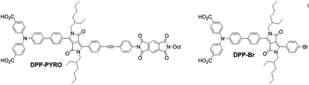 |
| | Fig. 4 The molecular structures of DPP-PYRO and DPP-Br dyes. | |
DPP-PYRO and DPP-Br also have more negative reduction potentials, −1.18 and −1.26 V vs. NHE, respectively, than P1 dye, rendering a large driving force to reduce an ETM, such as PCBM. To prove this, the dye was sensitized on the large band gap semiconductor Al2O3, on which the dye was not expected to inject either holes or electrons in Al2O3. By monitoring the photoluminescence (PL) quenching experiment of the dye on Al2O3 upon adding PCBM, PL quenching values of 85% and 70% were found for DPP-Br and DPP-PYRO, respectively; while that of the P1 dye was limited to around 30%. This proved that these two DPP dyes indeed had more efficient charge transfer to PCBM than the P1 dye.
With PCBM as the ETM, both DPP-Br and DPP-PYRO dyes showed higher VOC and JSC values than the P1 dye. Notably, the VOC obtained from P1 dye in this work, ca. 120 mV, was much lower than the value obtained in our previous work, 620 mV.16 The authors attributed this drop of VOC in their work to the poor quality of the NiO blocking layer according to dark current measurement, which indicated serious current leaking from the device. This implied that the performance of the DPP dye-based p-ssDSCs could be further improved by optimizing the blocking layer. The higher JSC values from these two dyes than that of P1 should be due to their efficient charge transfer reactions, since the P1 dye has a much larger extinction coefficient (by a factor of 2) than DPP-Br and DPP-PYRO. A DPP-Br based device rendered the highest performance among these dyes (Fig. 5), showing a JSC of 0.45 mA cm−2, a VOC of 198 mV, a fill factor (ff) of 0.32, and an overall efficiency of 0.028%. This is an important study to show the possibility of improving the p-ssDSCs performance by finely tuning the dye structure.
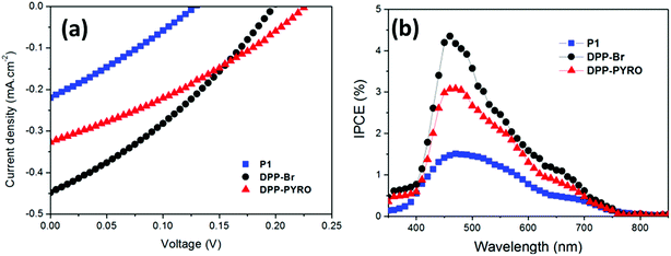 |
| | Fig. 5 The J–V curves (a) and IPCE spectra (b) of p-ssDSCs using DPP-PYRO, DPP-Br, and P1 dyes (adapted with permission from ref. 17. Copyright 2017 American Chemical Society). | |
Electron transport materials
The poor electron mobility of PCBM significantly limits the maximally obtainable efficiency of the p-ssDSCs. Reducing the PCBM layer thickness is not a practical solution to this problem, since a certain thick NiO film is always required in order to load enough dyes for efficient light harvesting. Alternatively, using an ETM with a high electron mobility instead of PCBM could enable great progress toward improving the performance of the p-ssDSCs. TiO2 has been successfully used as an n-type semiconductor (n-SC) in conventional n-DSCs, showing excellent performance even with a thickness of up to 10 μm.29 TiO2 film has shown an electron mobility of 0.01–0.1 cm2 V−1 s−1,30,31 which is 1–2 orders of magnitude higher than that of PCBM film. Moreover, TiO2 CB can have a potential of ca. −0.5 V vs. NHE at pH 7,32 which is similar to the reduction potential of PCBM, −0.4 V vs. NHE. Therefore, we proposed that TiO2 should be a good alternative ETM to PCBM in p-ssDSCs. However, considering the need for good pore filling in dye-sensitized NiO films, how to prepare TiO2 in an NiO film was a challenge to us. Solution-processing was the first method considered by us. Unfortunately, the commonly used solution-processable TiO2 precursor, titanium tetrachloride (TiCl4), is a strong acid. The dye became severely decomposed in our initial attempt when the dye-sensitized film was immersed into these compounds solutions for long time at a high temperature. Under these circumstances, we instead chose to use atomic layer deposition (ALD) to grow the TiO2 layer directly in the dye-sensitized NiO film18 as the ALD technique can use a short pulse of TiO2 precursor TiCl4 for the experiment and the temperature of formation of TiO2 can be mild. Still, to make sure the dye was stable during the ALD process, we abandoned the traditional p-type dyes containing a malononitrile acceptor, as we found such dyes showed a decrease in absorbance after ALD measurement more or less, probably due to the degradation of cyano units by the precursor of ALD TiO2 used in our experiment. Moreover, the conventional triphenylamine dyes with a malononitrile acceptor, such as P1-type dyes,9 have hardly distinguishable absorption spectra of its reduced and oxidized states, which is not a good sign for us to study charge-transfer processes in the device. Therefore, we synthesized PB6 dye (inset in Fig. 6a) using two carboxylic acid units as anchoring groups and perylene-monoimide (PMI) as an acceptor, which is thermostable and has distinguishable absorption spectra of its reduced (620 nm) and oxidized state (920 nm). PB6 dye can thermodynamically inject holes and electrons into NiO VB and TiO2 CB, respectively (Fig. 6b). Eventually, we had success preparing a PB6-sensitized nanoporous NiO film, in which a thin TiO2 layer was deposited by ALD to cover the dye on the NiO particles to maintain the nanoporous structure. The TiO2 layer as a shell could physically contact with the dye in this configuration. We therefore named it as dye-sensitized NiO-dye-TiO2 core–shell film.
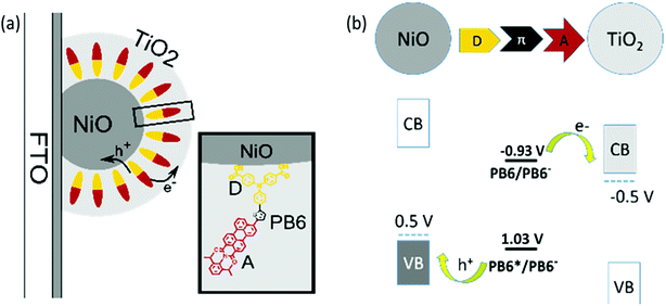 |
| | Fig. 6 (a) Schematic drawing of the well-orientated mesoporous NiO-dye-TiO2 core–shell structure and the donor–acceptor dye (PB6). (D) Electron-donor part, triphenylamine (TPA); (A) electron acceptor, perylene monoimide (PMI). (b) Potential diagram vs. NHE of PB6 between NiO and TiO2. (CB) Conduction band; (VB) valence band; (π) conjugated linker (ref. 18). | |
From scanning electron microscopy (SEM) images of a cross-section of the prepared NiO-dye-TiO2 film (Fig. 7), we could clearly distinguish FTO glass, the NiO blocking layer, and the nanoporous NiO layer. With help from energy-dispersive X-ray spectroscopy (EDX) mapping images, as shown in Fig. 7, we were able to observe the presence of Ti element across the entire NiO film. However, it is also obvious that there are more Ti element nearby the top region than close to the FTO surface. This implies that it is possible for ALD TiO2 to penetrate inside of the NiO nanoporous film, but the nanopores of the NiO film still limit the uniformity of the TiO2 layer formed. Unfortunately, we did not observe any crystalline structure of the TiO2 prepared by ALD in the NiO film, probably indicating that the prepared TiO2 on NiO particles in fact holds an amorphous structure (confirmed by TEM), or only a small portion are crystalline which could not be clearly observed.
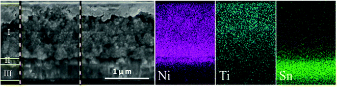 |
| | Fig. 7 SEM and EDX images of a cross-section of the NiO–PB6–TiO2 film: (I) mesoporous NiO layer coated by TiO2; (II) NiO blocking layer; (III) FTO layer, and the corresponding EDX element mapping analysis (ref. 18). | |
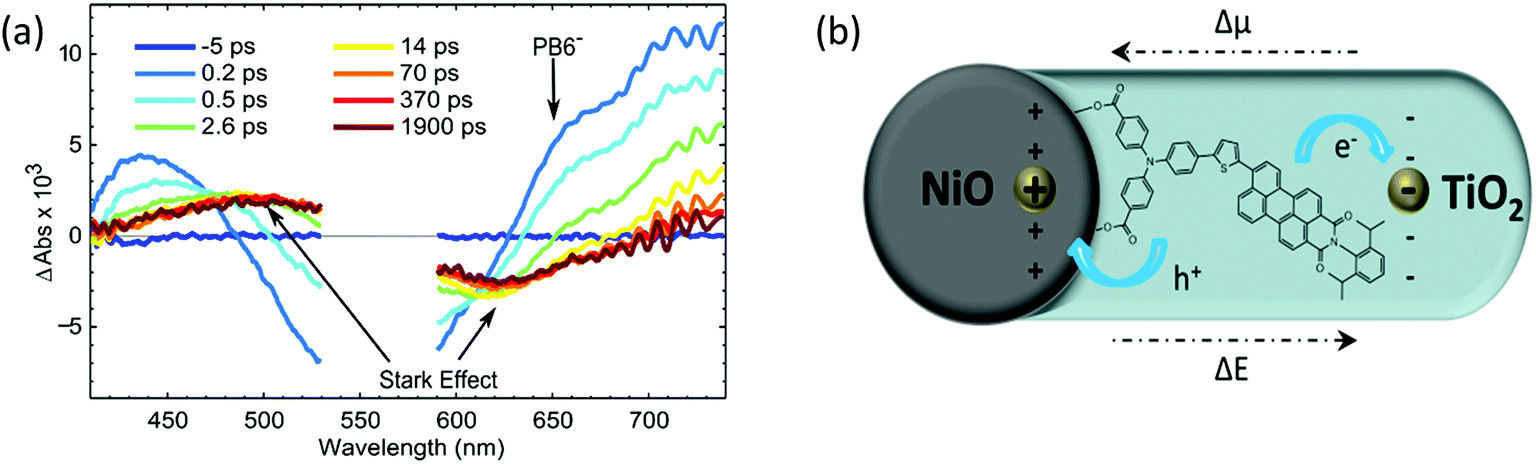
In order to investigate if the PB6 dye can kinetically perform charge separation into two different semiconductors upon light illumination, we used photon-induced absorption (PIA) spectroscopy and TAS to monitor the charge–separation processes or intermediators. Using ZrO instead of NiO, we were able to catch the oxidized PB6 in the presence of the ALD TiO2 layer from the PIA spectrum, indicating that the dye could inject electrons to TiO2 just through physical contact. In the NiO-dye-TiO2 system, formation of the reduced PB6 after hole injection into NiO from the excited dye could be clearly seen within 200 fs (Fig. 8a) in the TAS measurement. TAS produced pronounced spectra induced by the Stark effect due to an electrical field built between NiO and TiO2 after electron injection from the reduced dye into TiO2 (Fig. 8b). This process happened within 500 fs and lasted for more than 2 ns, suggesting that an ultrafast dye regeneration process and long-lived charge separation existed between NiO and TiO2.
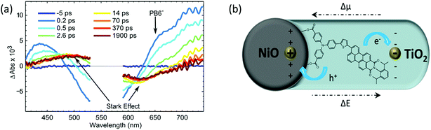 |
| | Fig. 8 (a) Transient absorption spectra of NiO–PB6–TiO2 film from −5 ps to 1.9 ns excited by a pulse laser of 560 nm, 300 nJ per pulse; (b) schematic drawing of the electric field formed after charge separation, Δμ is the difference in dipole moment and ΔE is the difference in the electrical field (ref. 18). | |
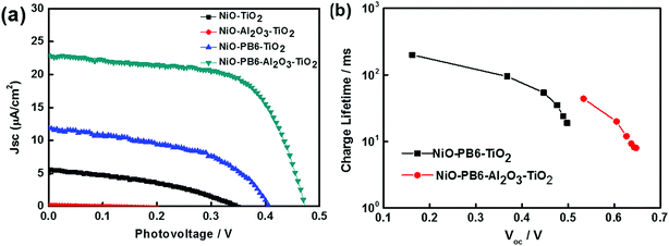
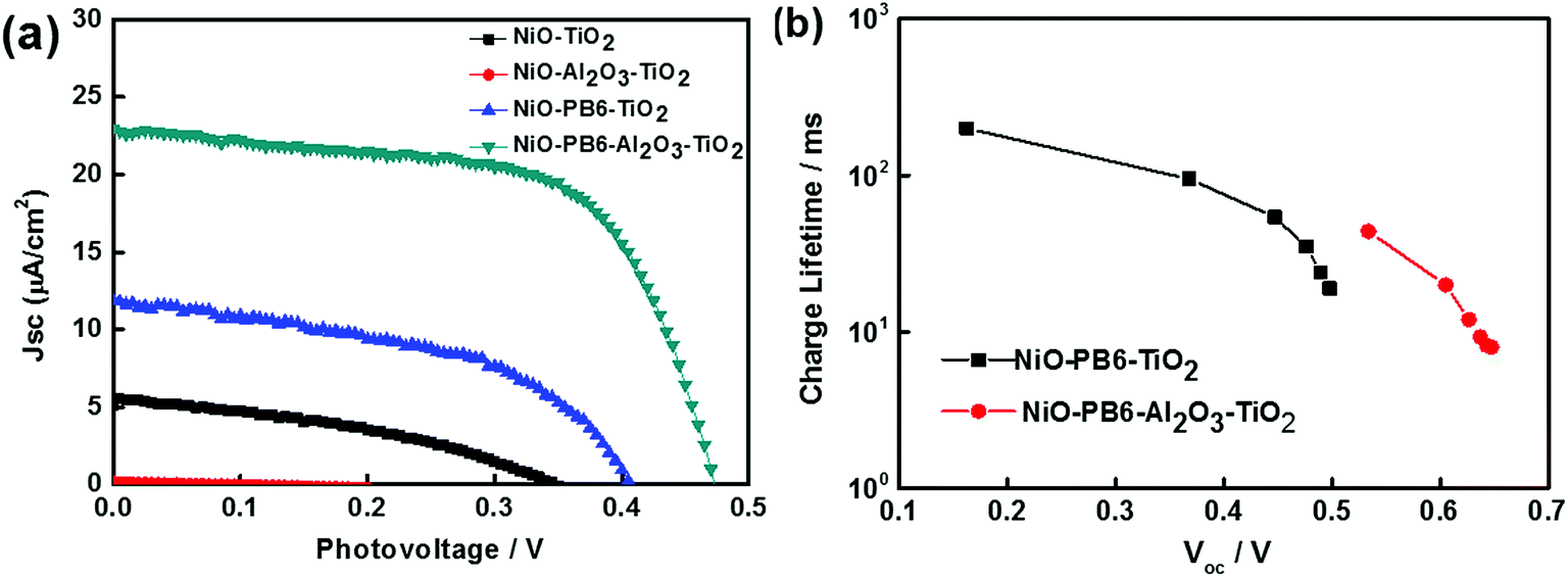
With these positive results, there was no doubt for us to move one step further to build p-ssDSCs by simply evaporating an Au layer as a back contact directly on the TiO2 layer in the core–shell film to collect electrons.19 The p-ssDSCs based on NiO–PB6–TiO2 indeed showed a photovoltaic effect (Fig. 9a). It rendered a VOC of 400 mV. However, the JSC was still low, only 12 μA cm−2. Considering that charge recombination was probably caused by direct contact between NiO and TiO2, we introduced a very thin (ca. 1 nm) Al2O3 layer after dye sensitization on NiO to isolate them and at the same time to protect the dye. Both the JSC and VOC of the p-ssDSCs based on NiO–PB6–Al2O3–TiO2 were significantly improved as compared to that of the NiO–PB6–TiO2-based devices. These improvements were attributed to the prolongation of the charge-separation lifetime in the presence of the inner barrier layer-Al2O3, as shown in Fig. 9b.
 |
| | Fig. 9
J–V curves of different NiO solar cells (a) and electron lifetime as a function of VOC density of NiO–PB6–Al2O3–TiO2- and NiO–PB6–TiO2-based p-ssDSCs (b) (ref. 19). | |
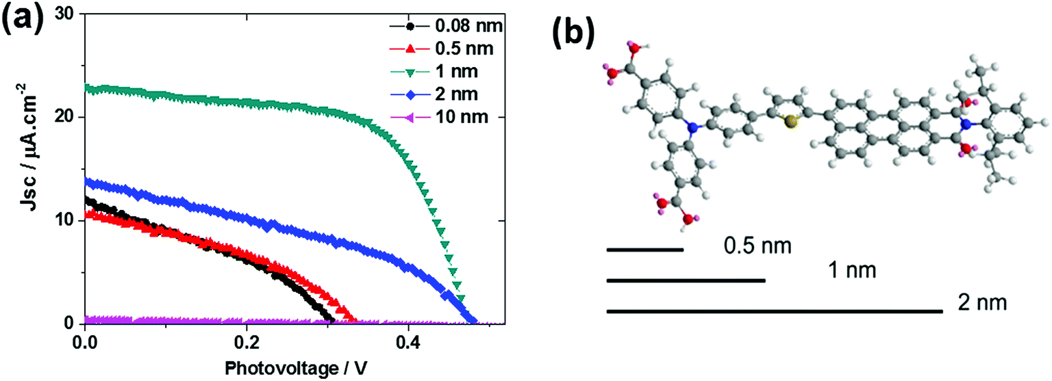
Interestingly, varying the thickness of the Al2O3 layer significantly influenced the solar cell performance (Fig. 10). The thickness of the Al2O3 layer was estimated from the ALD cycles. A 1 nm Al2O3 layer showed the optimal performance of the solar cell. From the molecular structure simulated from ChemDraw 3D, we concluded that an avg. 1 nm Al2O3 almost covers the donor moiety of the PB6 dye if the dye is assumed to stand on the NiO surface. Too thin an Al2O3 layer can not effectively suppress the charge recombination and too thick an Al2O3 layer completely buries the dye and makes it impossible to communicate with the TiO2 ETM layer, thus giving unsatisfactory performance.
 |
| | Fig. 10 (a) J–V curves for NiO–PB6–Al2O3–TiO2 solar cells with different Al2O3 thickness layers; (b) 3D molecular structure of PB6 with 0.5 nm, 1 nm, and 2 nm length scales as a comparison (ref. 19). | |
Although TiO2 as the ETM worked in p-ssDSCs, the performance of the device was still far behind what we expected. There were two main reasons for this: one is that the TiO2 layer prepared in NiO film was not crystalline, at least as proved from the TEM images, which limited the electron transport in the TiO2 layer; the other is that the TiO2 layer was not uniform, in which case the discontinuity of the TiO2 layer made electrons become trapped in the isolated TiO2 islands, resulting in a poor electron-collection efficiency. In order to address these issues, we attempted to use ZnO instead of TiO2 as the ETM in p-ssDSCs.20 ZnO can form a crystalline structure from a molecular complex at a much lower temperature than that needed for formation of the crystalline TiO2.33 Also, ZnO can be prepared by solution-processing from an organic dye-friendly compound, such as Zn(II) acetylacetonate (Zn(acac)2).33 The solution process is beneficial for improving the poor filling of NiO film and for having a continuous ZnO layer on the NiO surface. More important, ZnO film has shown excellent electron mobility of 1–10 cm2 V−1 s−1,34,35 which is 2–3 orders of magnitude higher than that of TiO2 film. Bearing these in mind, we fabricated the p-ssDSCs by using ZnO ETM prepared from a thermal method. The fabrication process is shown in Fig. 11. Notably, we could grow the ZnO layer in the NiO film in situ by sintering the spin-coated Zn(acac)2 at 200 °C. Thanks to the excellent thermal stability of the PB6 dye, there was no obvious degradation of the dye after thermally growing the ZnO layer. However, we had to use Al instead of Au as the back contact in the solution-processed ZnO-based p-ssDSCs, because we found the Au easily caused device short-circuit. The reason for this is still unclear at this moment. One hypothesis is that the solution-processed ZnO could not be as compact as the TiO2 layer prepared by ALD, thus giving a possibility for the heavy Au atoms to pass through and then contact with NiO, and maybe the FTO as well.
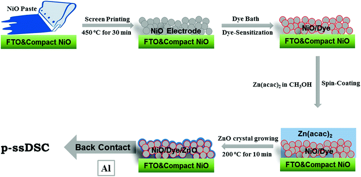 |
| | Fig. 11 Preparation process of p-ssDSCs based on NiO-dye-ZnO structure (reprinted and modified from ref. 20, with permission from Elsevier). | |
From the SEM and EDX mapping images of a cross-section of a NiO–PB6–ZnO solar cell (Fig. 12), we can clearly see different layers in the solar cell. In particular, we can see that the Zn element is uniformly spread across the entire NiO film, confirming that good infiltration of the ZnO precursor in the pores of NiO film can be obtained by the solution-processing method. Moreover, the formed ZnO was proved to be crystalline structure by TEM and X-ray powder diffraction (XRD) measurements. Excitingly, the p-ssDSCs using ZnO as the ETM showed an enhanced JSC of up to 680 μA cm−2, which was 60-fold higher than that of the previously reported device using TiO2 ETM with a similar architecture. Although the JSC of the NiO–PB6–ZnO solar cell was still lower than that of the liquid device using an identical NiO film, the VOC of the NiO–PB6–ZnO solar cell, 440 mV, was much higher than that of the liquid device, 120 mV. Eventually, the solid-state device rendered a higher efficiency of 0.135% than that of the liquid device, 0.106%. The p-ssDSCs with this configuration also showed good stability due to the sandwich structure in which the dye is well protected by two inorganic materials (Fig. 13).
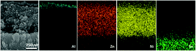 |
| | Fig. 12 Corresponding EDX element mapping analysis in the selected SEM cross-section range of the NiO–PB6–ZnO/Al-based solar cell device (reprinted and modified from ref. 20, with permission from Elsevier). | |
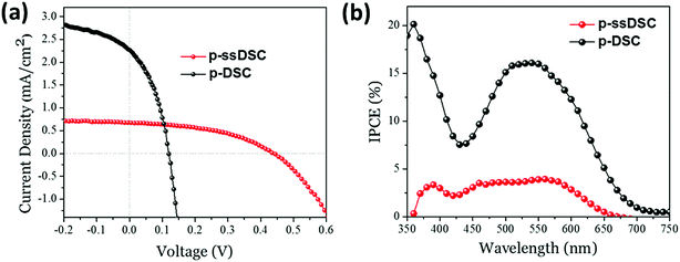 |
| | Fig. 13
J–V characteristics of the champion p-ssDSC and liquid p-DSC devices under 100 mW cm−2, AM 1.5G stimulated sunlight illumination (a) and corresponding IPCE spectra of the p-ssDSC and liquid p-DSC (b) (reprinted and modified from ref. 20, with permission from Elsevier). | |
Potential applications
In addition to the fabrication of p-ssDSCs, the dye-sensitized photocathodes with (p-SC)-dye-(n-SC) configuration have two more potential applications: dye-sensitized solar fuel devices (DSSFDs) and tandem solid-state dye-sensitized solar cells (t-ssDSCs).
(a) Dye-sensitized solar fuel device
Using the concept and configuration of DSCs to build up DSSFDs5–8 has been attracting more interest from scientists. In DSSFDs, the dye-sensitized photoanode is used to work with a catalyst for oxidation reactions, such as water oxidation, and the photocathode is adopted to work with a catalyst for reduction reactions, such as proton reduction and CO2 reduction. For the photoanode, it has reached 1.7 mA cm−2 photocurrent at a bias potential of 0.2 V vs. NHE for water oxidation.36 The performance of the photocathode for the reduction reaction is still too low to match the photocathode. In order to optimize the photocathode, catalysts and photosensitizers have been arranged on photocathodes by co-sensitization,37–39 using a supramolecule,40,41 and covalent linkage.9,42,43 However, few of them could significantly improve the performance for proton or CO2 reduction. Since hole injection from the dye into NiO has been proved as fast enough (ca. 200 fs) and the catalyst reduction from the reduced dye can be efficient and fast as well (ca. 10 ps),44 the low performance of the photocathode is in fact caused by the serious charge recombination, which is a consequence of slow hole diffusion in NiO and a slow catalytic cycle from the catalyst. However, the liquid p-DSCs using NiO still can generate a mA-scale photocurrent with a redox couple, which is much higher than the photocurrent obtained from the photocathodes for solar fuel production. Therefore, the main obstacle of the low photocatalytic current from photocathodes is due to the fast charge recombination between the reduced catalyst and the holes in NiO. Either prolongation of the charge separation between the reduced catalyst and holes in the NiO or the development of a more efficient catalyst could address the issue.
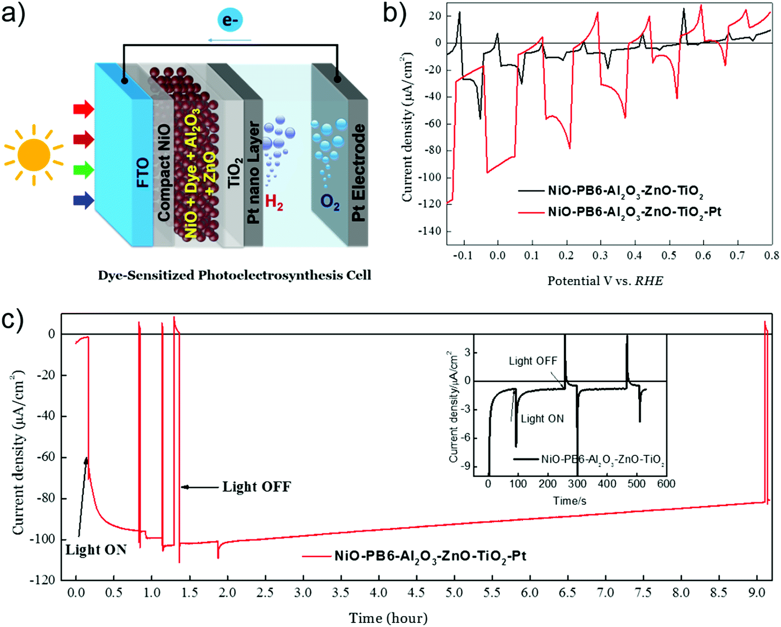
With the (p-SC)-dye-(n-SC) structure, we provide a possibility to build up an efficient photocathode for solar fuel production, as shown in Fig. 14. As the charges generated in dyes are initially separated by p-SC and n-SC and the separate holes and electrons have a long lifetime (>ns), this creates an opportunity to immobilize reduction catalysts directly on n-SC to receive electrons and perform catalytic reactions.20 Since the catalyst cannot touch the p-SC, the charge-recombination process, as we mentioned above, can be therefore suppressed. We proved the concept by putting Pt nanoparticles on our NiO-dye-ZnO photocathode for light-driven proton reduction. A thin Al2O3 layer and a compact TiO2 layer prepared by ALD were introduced to protect the dye and ZnO in acidic condition, respectively. We were able to obtain ca. 100 μA cm−2 photocurrent for hydrogen evolution at a mild bias potential of 0.05 V vs. reversible hydrogen electrode (RHE). The photocurrent only dropped by 20% after 9 h photoelectrocatalysis, rendering a faradaic efficiency of hydrogen evolution up to 100%. Although this proof-of-concept work used a precious metal catalyst, it also provides a possibility to integrate suitable low-cost molecular catalysts in this system.
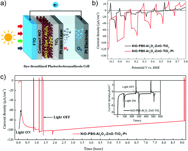 |
| | Fig. 14 (a) Device structure of a p-DSPEC; (b) linear sweep voltammetry (LSV) measurements of NiO–PB6–Al2O3–ZnO–TiO2 with Pt (red curve) and without Pt catalyst (black curve); (c) chronoamperometry measurement in a 0.1 M acetate buffer (pH = 5.0) under bias of 0.05 V vs. RHE: NiO–PB6–Al2O3–ZnO–TiO2–Pt photocathode (red curve); NiO–PB6–Al2O3–ZnO–TiO2 photocathode (the inserted image, black curve), LED white light illumination (420–750 nm), 50 mW cm−2, equivalent 1 sun condition from 420 nm to 750 nm (reprinted and modified from ref. 20, with permission from Elsevier). | |
(b) Tandem solid-state dye-sensitized solar cells
Tandem dye-sensitized solar cells (t-DSCs) with liquid redox couples have been reported.2,3 The theoretical VOC of the tandem solar cells is the sum of the photovoltage from both individual solar cells. Since the photoanode and photocathode in a liquid t-DSC share one redox couple, the
  is in principle determined by the energy difference between p-SC and n-SC (eqn (1)).
| |  | (1) |
where VOC,p is the open-circuit voltage of a p-type device; VOC,n is the open-circuit voltage of an n-type device; EVB,p is the VB level of p-SC; ECB,n is the CB level of n-SC, and Eredox is the redox potential of the redox couple.
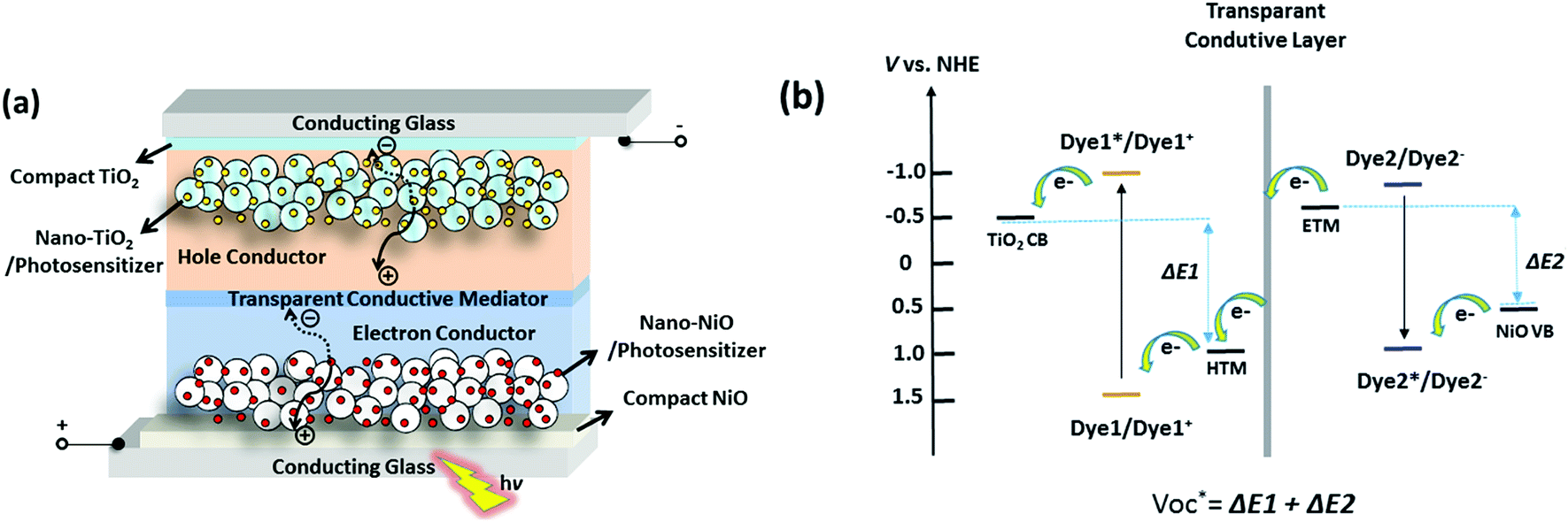
Using NiO as the p-SC and TiO2 as the n-SC in a liquid t-DSC, respectively, the  is ca. 1 V. With the p-ssDSCs, it is possible to make t-ssDSCs as shown in Fig. 15a, in which each photoelectrode has its own charge-transport material to collect charges and both photoelectrodes are connected by a transparent and conductive layer to perform inner charge transfer. With the transparent and conductive layer, this type of tandem device has a loss-free connection and in fact can be considered as a series connection of two individual solar cells obeying Kirchhoff's law. This kind of connection has been used in many types of solar cells to build up tandem devices.45–47
| |  | (2) |
where
EETM is the reduction potential of the electron-transport material for a p-type device and
EHTM is the oxidation potential of the hole-transport material for an n-type device. In this case, the

of the t-ssDSC can be more than 2 V with suitable charge-transport materials (
eqn (2) and
Fig. 15b). Making a rough calculation based on dyes on both photoelectrodes having complementary light absorption up to 850 nm, an efficiency of 18% can be obtainable from a t-ssDSC with a
VOC of 2 V, a
JSC of 12 mA cm
−2, and an ff of 0.75.
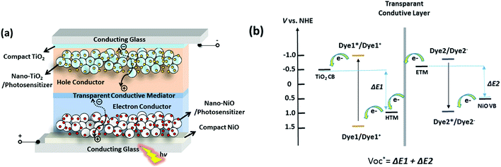 |
| | Fig. 15 Configuration (a) and potential diagram (b) of the proposed t-ssDSCs. | |
Challenges
To make efficient t-ssDSCs, improvement of the performance of the p-ssDSCs is desirable, since the photocurrent and efficiency of the p-ssDSCs are still far behind that of the conventional n-type ssDSCs (n-ssDSCs). One of major challenges is to seek new ETMs having high electron mobility and that can be prepared from solution-processing to giving good pore filling in the nanoporous p-SC film as well as to efficiently regenerate the dye. Non-fullerene organic ETMs can be considered in this scenario, since they have shown excellent performance as acceptors in organic solar cells and they can contribute photocurrent from light absorbing as well.48 Moreover, the development of new p-SCs with fast hole–transport properties and advanced dyes with broad absorption spectra and a high extinction coefficient can also help with improving the efficiency. Once the performance of p-ssDSC is significantly enhanced, the challenge left for t-ssDSCs is then how to connect the photocathode and the photoanode with a transparent and conductive layer without scarifying the individual photovoltaic parameters. For DSSFDs based on this kind of photocathode using molecular catalysts, matching the energy levels between the n-type semiconductor and the catalyst is crucial.
Conclusions
p-ssDSCs have been proposed and proven as functional devices for a few years. The photocurrent of the p-ssDSCs has been improved from an initial 50 μA cm−2 to ca. 1 mA cm−2. This implies that there is a possibility to further improve the performance of p-ssDSCs by tuning different components as well as by optimizing their configuration. Together with n-ssDSCs, p-ssDSCs can be used to develop solid-state tandem dye-sensitized solar cells (t-ssDSCs), which can render much higher photovoltage than that from conventional liquid tandem dye-sensitized solar cells. This has the potential to dramatically improve the efficiency of the solid-state dye-sensitized solar cells. A dye-sensitized photocathode using ZnO as the ETM has shown potential to contribute an efficient and stable device for light-driven hydrogen production. The preliminary results suggest that this type of photocathode is also good to improve the performance of dye-sensitized solar fuel devices (DSSFDs). Low-cost molecular catalysts are encouraged to be used in this kind of photocathode in follow up work. Still, there are many challenges still left behind in order to further improve the efficiency for both solar cells and solar fuel devices, as mentioned in this perspective.
Conflicts of interest
There are no conflicts to declare.
Acknowledgements
The author acknowledges the foundation support from the Swedish Energy Agency (43237-1). The author also thanks Sina Wrede (UU) for valuable discussion and comments and Lei Tian (UU) for providing some figures.
References
- J. He, H. Lindström, A. Hagfeldt and S.-E. Lindquist, J. Phys. Chem. B, 1999, 103, 8940–8943 CrossRef CAS.
- E. A. Gibson, A. L. Smeigh, L. Le Pleux, J. Fortage, G. Boschloo, E. Blart, Y. Pellegrin, F. Odobel, A. Hagfeldt and L. Hammarström, Angew. Chem., Int. Ed., 2009, 48, 4402–4405 CrossRef CAS PubMed.
- A. Nattestad, A. J. Mozer, M. K. R. Fischer, Y. B. Cheng, A. Mishra, P. Bauerle and U. Bach, Nat. Mater., 2010, 9, 31–35 CrossRef CAS PubMed.
- B. O'Regan and M. Gratzel, Nature, 1991, 353, 737–740 CrossRef.
- Z. Yu, F. Li and L. Sun, Energy Environ. Sci., 2015, 8, 760–775 RSC.
- H. Tian, ChemSusChem, 2015, 8(22), 3746–3759 CrossRef CAS PubMed.
- E. A. Gibson, Chem. Soc. Rev., 2017, 46, 6194–6209 RSC.
- D. L. Ashford, M. K. Gish, A. K. Vannucci, M. K. Brennaman, J. L. Templeton, J. M. Papanikolas and T. J. Meyer, Chem. Rev., 2015, 115, 13006–13049 CrossRef CAS PubMed.
- P. B. Pati, L. Zhang, B. Philippe, R. Fernández-Terán, S. Ahmadi, L. Tian, H. Rensmo, L. Hammarström and H. Tian, ChemSusChem, 2017, 10, 2480–2495 CrossRef CAS PubMed.
- H. Tian, J. Oscarsson, E. Gabrielsson, S. K. Eriksson, R. Lindblad, B. Xu, Y. Hao, G. Boschloo, E. M. J. Johansson, J. M. Gardner, A. Hagfeldt, H. Rensmo and L. Sun, Sci. Rep., 2014, 4, 4282 CrossRef PubMed.
- S. Du, P. Cheng, P. Sun, B. Wang, Y. Cai, F. Liu, J. Zheng and G. Lu, Chem. Res. Chin. Univ., 2014, 30, 661–665 CrossRef CAS.
- S. Powar, D. Xiong, T. Daeneke, M. T. Ma, A. Gupta, G. Lee, S. Makuta, Y. Tachibana, W. Chen, L. Spiccia, Y.-B. Cheng, G. Götz, P. Bäuerle and U. Bach, J. Phys. Chem. C, 2014, 118, 16375–16379 CrossRef CAS.
- M. Yu, T. I. Draskovic and Y. Wu, Phys. Chem. Chem. Phys., 2014, 16, 5026–5033 RSC.
- S. Powar, T. Daeneke, M. T. Ma, D. Fu, N. W. Duffy, G. Götz, M. Weidelener, A. Mishra, P. Bäuerle, L. Spiccia and U. Bach, Angew. Chem., Int. Ed., 2013, 52, 602–605 CrossRef CAS PubMed.
- I. R. Perera, T. Daeneke, S. Makuta, Z. Yu, Y. Tachibana, A. Mishra, P. Bäuerle, C. A. Ohlin, U. Bach and L. Spiccia, Angew. Chem., Int. Ed., 2015, 54, 3758–3762 CrossRef CAS PubMed.
- L. Zhang, G. Boschloo, L. Hammarstrom and H. Tian, Phys. Chem. Chem. Phys., 2016, 18, 5080–5085 RSC.
- T. T. T. Pham, S. K. Saha, D. Provost, Y. Farré, M. Raissi, Y. Pellegrin, E. Blart, S. Vedraine, B. Ratier, D. Aldakov, F. Odobel and J. Bouclé, J. Phys. Chem. C, 2017, 121, 129–139 CrossRef CAS.
- L. Tian, J. Föhlinger, P. B. Pati, Z. Zhang, J. Lin, W. Yang, M. Johansson, T. Kubart, J. Sun, G. Boschloo, L. Hammarström and H. Tian, Phys. Chem. Chem. Phys., 2018, 20, 36–40 RSC.
- L. Tian, J. Föhlinger, Z. Zhang, P. B. Pati, J. Lin, T. Kubart, Y. Hua, J. Sun, L. Kloo, G. Boschloo, L. Hammarström and H. Tian, Chem. Commun., 2018, 54, 3739–3742 RSC.
- B. Xu, L. Tian, A. S. Etman, J. Sun and H. Tian, Nano Energy, 2019, 55, 59–64 CrossRef CAS.
- P. Qin, H. Zhu, T. Edvinsson, G. Boschloo, A. Hagfeldt and L. Sun, J. Am. Chem. Soc., 2008, 130, 8570–8571 CrossRef CAS PubMed.
- R. Ganesamoorthy, G. Sathiyan and P. Sakthivel, Sol. Energy Mater. Sol. Cells, 2017, 161, 102–148 CrossRef CAS.
- V. D. Mihailetchi, J. K. J. van Duren, P. W. M. Blom, J. C. Hummelen, R. A. J. Janssen, J. M. Kroon, M. T. Rispens, W. J. H. Verhees and M. M. Wienk, Adv. Funct. Mater., 2003, 13, 43–46 CrossRef CAS.
- P. Morvillo, E. Bobeico, S. Esposito and R. Diana, Energy Procedia, 2012, 31, 69–73 CrossRef CAS.
-
L. Donggu, K. Junyoung, N. Seunguk and L. Changhee, 10th IEEE International Conference on Nanotechnology, 2010, pp. 1175–1178 Search PubMed.
- P. Qin, J. Wiberg, E. A. Gibson, M. Linder, L. Li, T. Brinck, A. Hagfeldt, B. Albinsson and L. Sun, J. Phys. Chem. C, 2010, 114, 4738–4748 CrossRef CAS.
- Y. Farré, L. Zhang, Y. Pellegrin, A. Planchat, E. Blart, M. Boujtita, L. Hammarström, D. Jacquemin and F. Odobel, J. Phys. Chem. C, 2016, 120, 7923–7940 CrossRef.
- L. Favereau, J. Warnan, Y. Pellegrin, E. Blart, M. Boujtita, D. Jacquemin and F. Odobel, Chem. Commun., 2013, 49, 8018–8020 RSC.
- S. Ito, S. M. Zakeeruddin, R. Humphry-Baker, P. Liska, R. Charvet, P. Comte, M. K. Nazeeruddin, P. Péchy, M. Takata, H. Miura, S. Uchida and M. Grätzel, Adv. Mater., 2006, 18, 1202–1205 CrossRef CAS.
- Y.-C. Tu, J.-F. Lin, W.-C. Lin, C.-P. Liu, J.-J. Shyue and W.-F. Su, CrystEngComm, 2012, 14, 4772–4776 RSC.
- W. S. Shih, S. J. Young, L. W. Ji, W. Water and H. W. Shiu, J. Electrochem. Soc., 2011, 158, H609–H611 CrossRef CAS.
- O. Ola, M. M. Maroto-Valer and J. Photochem, J. Photochem. Photobiol., C, 2015, 24, 16–42 CrossRef CAS.
- S. Musić, A. Šarić and S. Popović, Ceram. Int., 2010, 36, 1117–1123 CrossRef.
- P. Tiwana, P. Docampo, M. B. Johnston, H. J. Snaith and L. M. Herz, ACS Nano, 2011, 5, 5158–5166 CrossRef CAS PubMed.
- A. K. Chandiran, M. Abdi-Jalebi, M. K. Nazeeruddin and M. Grätzel, ACS Nano, 2014, 8, 2261–2268 CrossRef CAS PubMed.
- Y. Gao, X. Ding, J. Liu, L. Wang, Z. Lu, L. Li and L. Sun, J. Am. Chem. Soc., 2013, 135, 4219–4222 CrossRef CAS PubMed.
- L. Li, L. Duan, F. Wen, C. Li, M. Wang, A. Hagfeldt and L. Sun, Chem. Commun., 2012, 48, 988–990 RSC.
- L. J. Antila, P. Ghamgosar, S. Maji, H. Tian, S. Ott and L. Hammarström, ACS Energy Lett., 2016, 1, 1106–1111 CrossRef CAS.
- C. E. Creissen, J. Warnan and E. Reisner, Chem. Sci., 2018, 9, 1439–1447 RSC.
- Z. Ji, M. He, Z. Huang, U. Ozkan and Y. Wu, J. Am. Chem. Soc., 2013, 135, 11696–11699 CrossRef CAS PubMed.
- B. Shan, A. K. Das, S. Marquard, B. H. Farnum, D. Wang, R. M. Bullock and T. J. Meyer, Energy Environ. Sci., 2016, 9, 3693–3697 RSC.
- N. Kaeffer, J. Massin, C. Lebrun, O. Renault, M. Chavarot-Kerlidou and V. Artero, J. Am. Chem. Soc., 2016, 138, 12308–12311 CrossRef CAS PubMed.
- H. Kumagai, G. Sahara, K. Maeda, M. Higashi, R. Abe and O. Ishitani, Chem. Sci., 2017, 8, 4242–4249 RSC.
- A. M. Brown, L. J. Antila, M. Mirmohades, S. Pullen, S. Ott and L. Hammarström, J. Am. Chem. Soc., 2016, 138, 8060–8063 CrossRef CAS PubMed.
- T. Ameri, G. Dennler, C. Lungenschmied and C. J. Brabec, Energy Environ. Sci., 2009, 2, 347–363 RSC.
- T. Todorov, T. Gershon, O. Gunawan, Y. S. Lee, C. Sturdevant, L.-Y. Chang and S. Guha, Adv. Energy Mater., 2015, 5, 1500799 CrossRef.
- S. H. Moon, S. J. Park, S. H. Kim, M. W. Lee, J. Han, J. Y. Kim, H. Kim, Y. J. Hwang, D.-K. Lee and B. K. Min, Sci. Rep., 2015, 5, 8970 CrossRef CAS PubMed.
- C. Yan, S. Barlow, Z. Wang, H. Yan, A. K. Y. Jen, S. R. Marder and X. Zhan, Nat. Rev. Mater., 2018, 3, 18003 CrossRef CAS.
|
| This journal is © The Royal Society of Chemistry 2019 |
Click here to see how this site uses Cookies. View our privacy policy here. 
 Open Access Article
 This Open Access Article is licensed under a
  *
*


 of the tandem solar cells is the sum of the photovoltage from both individual solar cells. Since the photoanode and photocathode in a liquid t-DSC share one redox couple, the
  is in principle determined by the energy difference between p-SC and n-SC (eqn (1)).
 is ca. 1 V. With the p-ssDSCs, it is possible to make t-ssDSCs as shown in Fig. 15a, in which each photoelectrode has its own charge-transport material to collect charges and both photoelectrodes are connected by a transparent and conductive layer to perform inner charge transfer. With the transparent and conductive layer, this type of tandem device has a loss-free connection and in fact can be considered as a series connection of two individual solar cells obeying Kirchhoff's law. This kind of connection has been used in many types of solar cells to build up tandem devices.45–47
 of the t-ssDSC can be more than 2 V with suitable charge-transport materials (eqn (2) and Fig. 15b). Making a rough calculation based on dyes on both photoelectrodes having complementary light absorption up to 850 nm, an efficiency of 18% can be obtainable from a t-ssDSC with a VOC of 2 V, a JSC of 12 mA cm−2, and an ff of 0.75.