Plasmonic noble metal@metal oxide core–shell nanoparticles for dye-sensitized solar cell applications
Received
9th July 2018
, Accepted 14th September 2018
First published on 14th September 2018
Abstract
The aim of this review is to summarize recent advances in the field of dye-sensitized solar cells (DSSCs) utilizing plasmonic nanoparticles (NPs), where the effect of plasmonic NPs in terms of size, shape, and composition on the overall efficiency has been taken into account. Various approaches for size and shape-controlled synthesis of plasmonic NPs (typically Ag or Au NPs) have been discussed. Plasmonic NPs are found to be unstable in iodide based redox electrolytes commonly used in DSSCs and high temperature sintering during photoanode preparation. Therefore, plasmonic NPs are encapsulated with metal oxides, specifically TiO2 or SiO2 NPs, to form core–shell structures in order to improve their chemical and thermal stability. The synthesis process and optical characteristics of plasmonic core–shell NPs are discussed in detail. Incorporation of plasmonic core–shell NPs has improved the light harvesting capability of the photoanode and hence significantly improved the performance of DSSCs. Plasmonic core–shell NPs have also decreased the amount of active material required to attain high efficiency. The surface plasmon resonance (SPR) of plasmonic NPs is tuned by varying their size, shape or shell thickness and composition for better overlapping with the absorption spectrum of the sensitizer in order to further improve the light harvesting capability. The factors responsible for the enhancement in the performance of plasmonic DSSCs, such as resonant energy transfer, hot electron injection, and local electromagnetic field enhancement, are discussed in detail. Finally, the existing challenges in the field of DSSCs and future prospects to solve these problems in order to further improve the solar energy conversion are also discussed.
 Prabhakar Rai | Prabhakar Rai is an INSPIRE Faculty member in the Department of Chemical Engineering at the Indian Institute of Technology Kanpur, India. Previously, he was a Research Professor (2013–2014) in the Department of Materials Science and Engineering at Korea University and an Assistant Research Professor (2012–2013) in the Department of Informatic Electronic Materials Engineering at Chonbuk National University, South Korea. He received his Doctoral degree (2012) in Informatic Electronic Materials Engineering from Chonbuk National University, South Korea. He was a Visiting researcher (2018) at the Research Center on Engineering of Materials and micro/nanoSystems (EMaS) at Universitat Rovira i Virgili, Spain. His research is mainly focused on synthesis of nanoscale noble metal@metal oxide core@shell for energy (electrochemical supercapacitors and dye-sensitized solar cells) and environmental (gas sensors and bio-sensors) applications. |
1. Introduction
The current energy crisis spurs us on to find a new pollution-free, sustainable energy source. Since a photovoltaic cell converts solar radiation directly into electrical energy, it is considered as the most promising renewable resource.1 First generation solar cells, having higher efficiency than other solar cells, are made up of monocrystalline silicon wafers; however their fabrication cost is very high. Thin film solar cells (such as CdTe, CIGS or a-Si), also called second generation solar cells, are less expensive than first generation solar cells but they suffer from poor efficiency. DSSCs having moderate efficiency ∼10 are considered as the third generation of solar cells and they are relatively cheaper than the other two kinds of solar cells. Therefore, many efforts have been devoted to the development of DSSCs after their discovery by O’Regan and Graetzel in 1991.2 DSSCs are composed of four major components, namely a semiconductor coated photoanode, a counter electrode, a sensitizer and an electrolyte as shown in Fig. 1.3 The photoanode is composed of dye-sensitized TiO2 coated on fluorine-doped tin oxide (FTO), whereas the counter electrode is composed of platinum (Pt) sputtered onto a FTO substrate. The working electrode and counter electrode are separated from an electrolyte solution (typically, I−/I3−) to facilitate the charge transport between these two electrodes and help the regeneration of dye molecules. When a DSSC is illuminated, dye molecules get excited by absorbing in the visible spectrum which is followed by the injection of excited electrons from dye molecules into the conduction band of TiO2. The injected electrons travel through the working electrode to an external load and finally reach the counter electrode to complete the circuit, and hence the DSSCs generate electricity when illuminated with solar light. At the end of the cycle, electrons are transferred from the electrolyte to dye molecules at the counter electrode to regenerate the oxidized dye and to continue the process in a cyclic manner.4
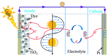 |
| | Fig. 1 Schematic representation of the components and of the basic working principle of DSSCs. | |
In the last two decades, DSSCs have been intensively investigated in almost every aspect, even though the best power conversion efficiency (PCE) of DSSCs is still much lower (∼13%) than that of silicon solar cells.5 Several attempts have been made to improve the PCE by utilizing different dyes,6–8 quantum dots,9,10 active layer materials of different morphologies,11–13 or novel electrolyte solutions,14 but these efforts have marginally improved the efficiency of DSSCs.15 The low PCE of DSSCs is mainly related to poor light absorption capability of metal oxides (TiO2 can absorb light mainly in the UV region) and dye molecules (ruthenium based dye absorbs light in the visible region).16 The incorporation of plasmonic NPs, such as Ag and Au NPs, into photovoltaics appears to be a highly promising strategy for the improvement of PCE.17,18 It has been found that plasmonic NPs absorb light via the collective oscillations of surface electrons, which can be excited and directly injected into the conduction band of semiconductors.18 Furthermore, the poor light absorption capability of TiO2 can also be extended through the enhancement of the photoabsorption cross section of dye molecules.19 In addition, the formation of Schottky barriers at the interface of metal oxide and metal NPs can significantly reduce the recombination rate of photo-excited electron–hole pairs.20 Therefore, plasmonic NPs of different morphologies showing tuned SPR characteristics have been tested for the PCE enhancement of DSSCs.19–22 Although the incorporation of bare plasmonic metal NPs has improved the PCE of DSSCs, the use of corrosive iodide-based liquid electrolytes results in reduced long-term stability, unless metal NPs are protected.23–25 Therefore, core–shell nanostructures having a noble metal core and metal oxide shell have gained immense attention in various applications including DSSCs due to their unique physical properties with high thermal and chemical stability.24–30
Several review articles have been published on plasmonic solar cells; however reviews outlining the utilization of plasmonic noble metal@metal oxide core@shell NPs in DSSCs are rarely available.24,25 The existing reviews have been focused mainly on the fundamental physics of interfacial structures.24,25,31 However, in this review article, I present an overview of the recent research on synthesis procedures, optical characteristics and applications of plasmonic metal@ metal oxide core–shell NPs for DSSCs. In the first section, the fundamental physics of plasmonic NPs in relation to DSSCs is discussed. The second section includes the preparation methods and structural characteristics of different noble metals and their core–shell structures with metal oxides primarily used in DSSCs. The effect of size, shape, shell thickness, and composition of plasmonic core–shell NPs on DSSC performance is discussed in the third segment. Finally, we conclude with a perspective on the emerging challenges and future developments in DSSCs.
2. Basics of plasmonics in relation to DSSCs
Plasmonics is a broad area of physics and the detailed discussion of it is beyond the scope of this review article. Here, I discuss plasmonics in relation to DSSCs as the geometry and surrounding medium around metal NPs affect their SPR.32–35 SPR is a quantum optical-electrical phenomenon and confined to surfaces of metal. It occurs at the interface of a material which possesses a negative real and small positive imaginary dielectric constant, for instance, a metal and a dielectric (Fig. 2a). SPR arises due to the coherent oscillation of the surface conduction electrons of metals, called plasmons, when excited with electromagnetic radiation.32 SPR mainly depends on the metal characteristics, the refractive index of the media, the wavelength of the incident light, and temperature.33
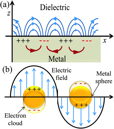 |
| | Fig. 2 Schematic diagrams illustrating (a) SPP and (b) LSPR. | |
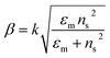
The excitation of SPR on the plane metallic surface is propagating in nature and hence called surface plasmon polariton (SPP). However, the excitation of SPR on NPs is localized and hence called localized SPR (LSPR). The propagation constant of the surface plasmon wave is given by eqn (1),
| |  | (1) |
where ‘
k’ symbolizes the free space wave number, ‘
εm’ the dielectric constant of the metal (
εm =
εmr + i
εmi, real and imaginary components, respectively) and ‘
ns’ the refractive index of the dielectric. This equation suggests that the surface plasmon waves can be supported by the structure if
εmr < −
ns2. Therefore, propagating and non-propagating excitation of SPR can be tailored in the desired range of wavelengths by changing the metal nano-geometries. Since, LSPR frequency depends on the intrinsic dielectric properties of a given metal and hence any variation in the shape or size of metal NPs which can alter the surface polarization results in a change in the LSPR.
33 The recent advances in the morphologically controlled synthesis of metal NPs have led researchers to demonstrate the advantage of SPR in several applications including DSSCs.
34,36–38
2.1 Localised surface plasmon resonance (LSPR)
Metallic NPs strongly scatter and absorb the incident light due to their LSPR and frequency of LSPR primarily depends on the free electron density in the NPs. As shown in Fig. 2b, the plasmon is oscillating in phase with the electric field of incident light which generates electromagnetic hot-spots at the poles of the NPs.32 The dipole polarizability (α) of spherical NPs with size much smaller than the wavelength of the light is given by eqn (2):| | 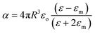 | (2) |
where ‘R’ is the NP radius and ‘εo’ is the free space permittivity. Such NPs exhibit a dipolar LSPR when the denominator diminishes as given by eqn (3):where ‘εr’ denotes the real part of ‘ε’, expressed as a function of the frequency of light ‘ω’ by the Drude model as given by eqn (4):| |  | (4) |
where ‘ωp’ is the bulk plasma oscillation frequency associated with the free carriers and ‘γ’ is their bulk collision frequency. From eqn (3) and (4), we get the frequency ωsp at which the resonance conditions are described by eqn (5):| | 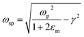 | (5) |
where ωsp represents the LSPR energy and γ represents the line width of the LSPR band.
The LSPR of noble metal NPs, especially Ag and Au fall in the infra-red (IR) to visible region, which perfectly matches with the absorption spectrum of TiO2 and dye molecules used in DSSCs.35 Therefore, these metallic NPs are widely used for PCE enhancement of DSSCs. It is noteworthy that in order to permit the transfer of energy from photons to plasmons, the energy and momentum of both must match exactly.39
2.2 Factors affecting LSPR
The LSPR frequency depends on the intrinsic dielectric properties of a given metal, dielectric constant of the medium in contact with the metal, and pattern of surface polarization.33 Thus, any variation in the shape or size of metal NPs which can alter the surface polarization results in a change in the LSPR. Therefore, the knowledge of various factors which can affect the LSPR is very important for their practical application in DSSCs.
2.2.1 Metal NPs.
For LSPR, a metal must have conduction band electrons which can interact with light at a suitable wavelength. A variety of metals, such as silver (Ag), gold (Au), copper (Cu), and aluminium (Al), exhibit the LSPR phenomenon. The bulk plasma frequency ‘ωp’ depends on the carrier (holes) density ‘Nh’ as given in eqn (6):| |  | (6) |
where ‘mh’ is the hole effective mass, approximated to be 0.8m0 where ‘m0’ is the electron mass. Thus the LSPR frequency for a sphere in free space mainly depends on the density of free electrons in the NPs and occurs at  . The order of electron densities for different metals is related to the region of the light spectrum in which resonance occurs. For example, Ag has higher free electron density as compared to Au which results in LSPR in the ultra-violet region for Ag as compared to the visible region for Au.40,41
2.2.2 Size of metal NPs.
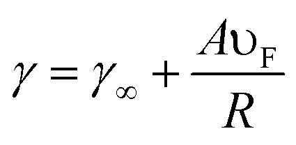
The size of NPs considerably affects their optical and electronic properties due to the quantum confinement of the conduction electrons.42 The size of the NPs influences the relative magnitude of the absorption and scatter cross section. The size dependence of the LSPR frequency can be described by eqn (7)| |  | (7) |
where ‘γ∞’ is the scattering rate of the free electrons in bulk metal, ‘A’ is a constant, ‘υF’ is the Fermi velocity of the electrons, and ‘R’ is the radius of the NPs. From eqn (7) it is clear that the absorption wavelength is directly proportional to the radius of NPs, and hence as the NP size decreases the LSPR wavelength also decreases. The increase in frequency with the decrease of the NP size is caused by the scattering of the conduction electrons on the surface of the NPs.43 It is noteworthy that this relationship depends only on size and is independent of the aspect ratio of the NPs. However, Peng et al. found that the absorption peak of Ag NPs blue-shifted as the particle size decreased from 20 to 12 nm and red-shifted with a further decrease in size.44 Weick et al. explained that this behavior arises due to the interaction of conduction electrons with the electrons in deeper bands and a spill-out effect.45 Pathak et al. found only one resonance peak in small size metal NPs and multiple peaks in larger NPs due to radiation effects in larger metal NPs as charge density becomes asymmetric.46 In our previous study, we found that the LSPR band was red-shifted and absorption intensity was decreased with an increase in the size of Ag NPs from 15 to 40 nm.47 The decrease in absorption intensity with the increase in particle size can be explained by eqn (8).| | A = (NσabsL/ln![[thin space (1/6-em)]](https://www.rsc.org/images/entities/char_2009.gif) 10) 10) | (8) |
where A, N, σabs, and L are the absorbance, number of particles per unit volume, absorption cross section, and the optical path length, respectively. Thus, absorption intensity decreases as the number of particles per unit volume decreases due to the increase in particle size.
2.2.3 Shape of metal NPs.
The shape of metallic NPs can change the surface polarization, and therefore LSPR at desired wavelengths can be achieved by shape-controlled syntheses, such as nanorods, nanoprisms, nanocubes, octahedrons, etc.33,48–50 The relationship between the SPR shift and shape of particles can be established by eqn (9)51| | 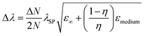 | (9) |
where ‘N’ is the electron density in the metals, ‘λsp’ is the SPR wavelength for metals, ‘ε∞’ is the high-frequency contribution to the metal dielectric function, ‘εmedium’ is the dielectric constant of the medium, and ‘η’ is the particle shape factor. The energy distribution ‘δN’ of hot-carriers was found to be proportional to the field enhancement factor ‘k’ inside the NPs as given in eqn (10).52| |  | (10) |
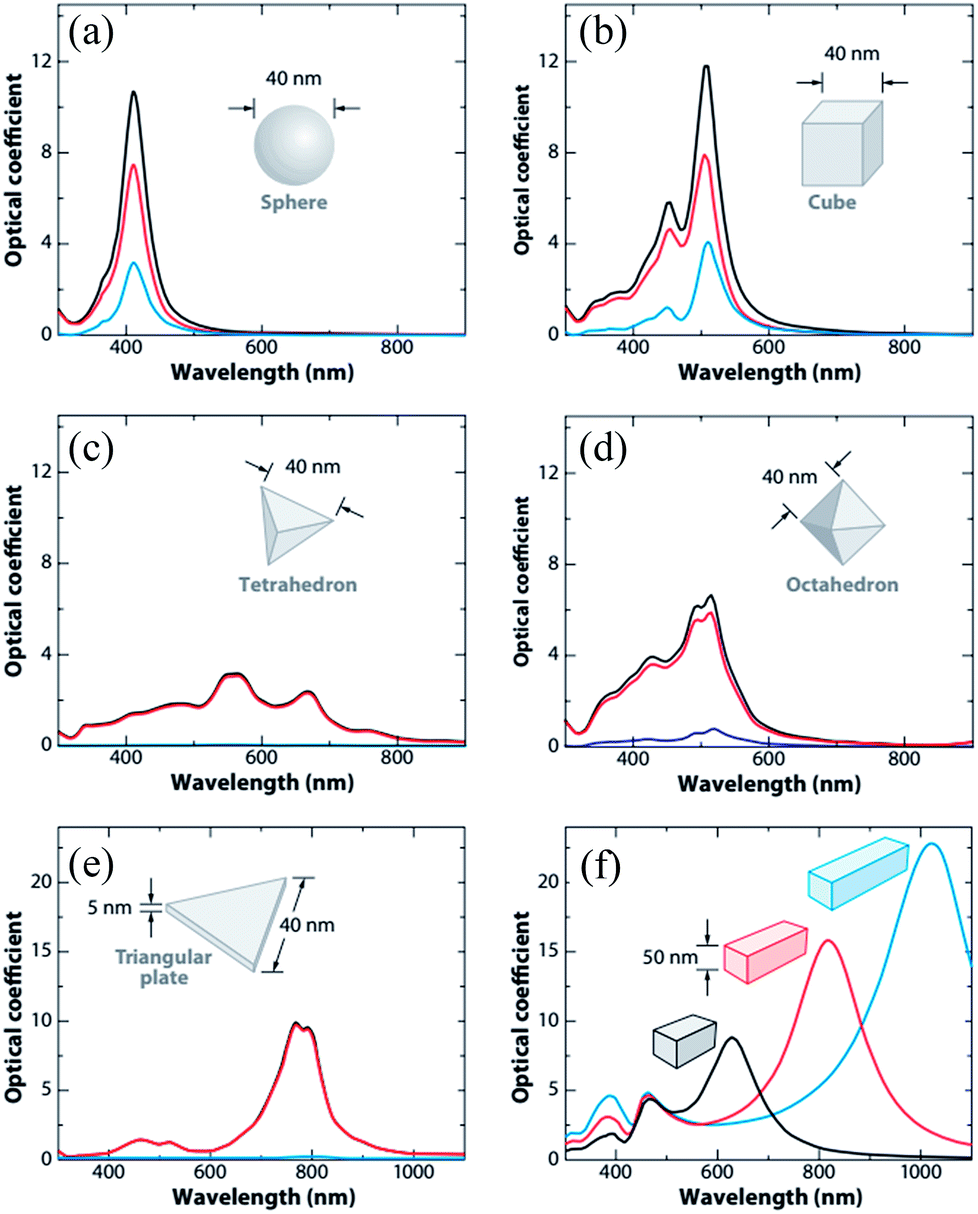
Since ‘k(ω)’ follows the behavior of the polarizability and hence ‘k’ is shape-dependent, the hot-carrier generation is also affected by the shape of the metallic NPs.53 If the edge length or sharpness of NPs are increased, then a red-shift in LSPR is observed, which is attributed to the increase in charge separation. Meanwhile, if the symmetry of NPs is increased, then an increase of LSPR intensity is observed.54 Furthermore, non-spherical NPs can be polarized in a number of modes, and hence a similar number of LSPR peaks can be found in absorption spectra.55–57 For example, nanorods can be polarized along two axes i.e. transverse and longitudinal, and hence exhibit two LSPR peaks.48 Thus, non-spherical NPs show multiple, red-shifted peaks in absorption spectra as compared to spherical NPs, as illustrated by Fig. 3.
 |
| | Fig. 3 Extinction (black), absorption (red), and scattering (blue) spectra calculated for Ag nanoparticles of different shapes: (a) a sphere displaying a single dipole resonance peak and (b) a cube, (c) a tetrahedron, (d) an octahedron, and (e) a triangular plate. (f) Extinction spectra of rectangular bars with aspect ratios of 2 (black), 3 (red), and 4 (blue). Note that the nonspherical particles typically exhibit multiple, red-shifted resonance peaks. Reprinted with permission from ref. 48. Copyright 2009 Annual Reviews. | |
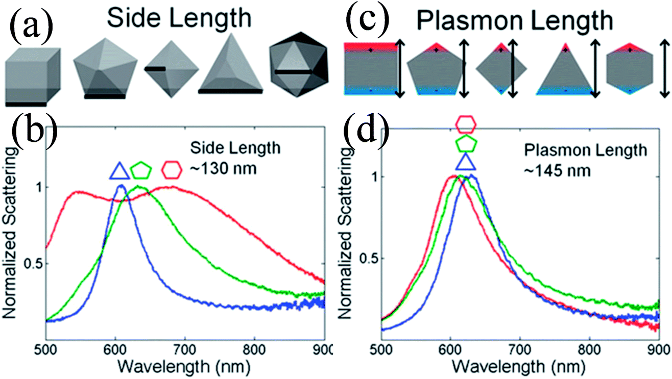
Duyne and co-workers explained that variation in the LSPR of non-spherical NPs is shape-independent and depends on the plasmon length (Fig. 4).58 The plasmon length is defined as the distance between regions of opposite charge in dipolar plasmons created by plasmonic electron oscillation, as illustrated in Fig. 4c. They found that NPs having similar plasmon lengths show similar LSPR spectra, although their shape was different (Fig. 4d). However, this approach is limited only to those NPs having a fixed aspect ratio and well-formed vertices. It is important to note that any change in the NP shape affects the LSPR peak position to a greater extent as compared to size. For instance, only a 47 nm red-shift is found in absorption spectra when spherical NP size was increased from 10 to 100 nm, whereas 92 nm shifts was recorded for elliptical NPs when their aspect ratio was changed from 2.5 to 3.5.59
 |
| | Fig. 4 Comparison between the side length and plasmon length as descriptors of NP size. (a) Definition of the side length of the shapes analyzed. (c) Definition of the plasmon length. (b and d) Representative single-particle spectra for Au triangles (blue), decahedra (green), and icosahedra (red) of a similar side (b) or plasmon length (d). Reprinted with permission from ref. 58. Copyright 2012 American Chemical Society. | |
2.2.4 Surrounding medium.
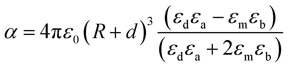
LSPR is highly sensitive to the surrounding medium and its absorption wavelength maximum ‘λmax’ changes as the dielectric constant ‘ε’ or refractive index ‘n’ of the medium is changed.60–62 Chang et al. studied the effect of surrounding media on the LSPR of Au nanorods using air (n = 1), water (n = 1.3), and oil (n = 1.5) as the medium.62 They found that the SPR peak was red-shifted with an increase in the refractive index of the medium and vice versa. Thus, the LSPR frequency can be shifted by varying the dielectric constant of plasmonic core–shell NPs. The field induced by plasmonic core – dielectric shell NPs can be written in the form of effective polarisability and dipole moment as given by eqn (11).63where ‘p’ is the effective dipole moment of the core–shell system, ‘E0’ is the incident electric field, ‘α’ is the dipolar polarisability and ‘εm’ is the dielectric constant of embedding media. When the NPs are coated with a dielectric material of thickness ‘d’ and dielectric constant ‘εd’, then polarizability is defined by eqn (12).| | 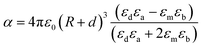 | (12) |
where ‘a’ is the core radius and εa is the dielectric constant of the core. Similarly, ‘b’ is the total radius of the core–shell system and εb is the dielectric constant of the core–shell system. Thus, a red-shift in absorption spectra is observed with the increase in the dielectric constant of the environment. It is attributed to the accumulation of polarization charges on the dielectric that weakens the restoring force within NPs. The magnitude of the spectral shift for NPs is described by eqn (13);| | | Δλmax = mΔn [1 − exp(−2d/ld)] | (13) |
where ‘m’ is the bulk refractive-index response of the NPs, ‘Δn’ is the change in the refractive index induced by the adsorbate, ‘d’ is the effective adsorbate layer thickness, and ‘ld’ is the characteristic electromagnetic field decay length. Thus, shell materials with a higher refractive index will lead to a larger red-shift with broadening of LSPR peaks.47,49,64–67 For example, we have studied the effect of shell thickness on the LSPR of Au@SnO2 core–shell NPs and found that the LSPR peak was red-shifted from 540.5 to 576.5 nm with an increase in shell thickness from ∼7 nm to ∼20 nm (Fig. 5).67
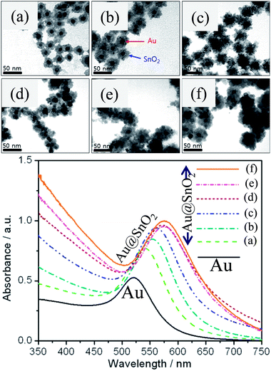 |
| | Fig. 5 TEM images of Au@SnO2 core–shell NPs with different shell thicknesses, (a) ∼8, (b) ∼10, (c) ∼12, (d) ∼15, (e) ∼17, and (f) ∼20 nm and corresponding UV visible spectra. Reprinted with permission from ref. 67. Copyright 2015 Elsevier. | |
2.2.5 Temperature of metal NPs.
In addition, the temperature of NPs also affects their LSPR as the scattering rate of the free electrons in bulk metals depends on the temperature γ∞ = γ∞(T). The increase in temperature leads to a red-shift of the SPR mainly because the electron-phonon scattering increases with an increase in phonon population in the metal NPs. However, Yeshchenko et al. found SPR linearly red-shifted with the increase of temperature for large Ag NPs (25 and 30 nm), and non-linearly for smaller NPs (17 and 11 nm).42 This phenomenon is attributed to the coefficient of the volume of thermal expansion, which increases with a decrease of NP size and increase of temperature. Mock et al. studied morphological and spectral changes of triangular Ag NPs as a function of heat treatments.54 They found that the spectral peak centered at 625 nm blue-shifted to 585 nm after heating for 30 min at 200 °C due to rounding of triangular corners. Thus, a simple heat treatment can modify the particle shape as well as SPR properties. Similarly, Cetin et al. applied temperature to tune the refractive index of the surrounding medium to tune the SPR band. The change in temperature from 15 to 33 °C changed the refractive index by ≈0.0317, and thus changed the SPR wavelength by ≈19 nm.68
2.3 Surface plasmon decay
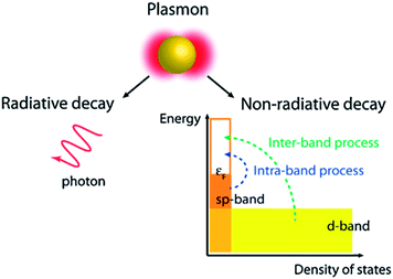
SPR decay takes place in two ways, i.e. radiative (far-field scattering/radiative damping) or non-radiative (near-field/absorption/exciton generation, typically referred to as hot carriers) as displayed in Fig. 6.69,70 It has been found that only non-radiative damping occurs in the metallic film with SPPs, whereas both radiative and non-radiative decay competitively occur in NPs with LSPR properties. It is important to note that the radiative process related to the scattering cross section of the NPs remains insignificant for small NPs and becomes significant with an increase in their dimensions. In non-radiative damping, the plasmon is converted into electron–hole pairs by inter-band (d band) and intra-band (SP band) excitations. As compared to the radiative process, non-radiative processes are size-independent as they are determined by the nanostructure's band structure. However, an inter-band process requires sufficient plasmon energy to excite d-band electrons beyond the Fermi level. It is noteworthy that plasmons decay much slowly through non-radiative processes in nanostructures resonating in the NIR region, and thus plasmon decay in nanorods is much slower than in NPs. Therefore, photo-excited hot-carriers in metals can either be directly used to drive chemical reactions, or transferred to a semiconductor for use in photovoltaics and photoelectrochemical systems.71–73
 |
| | Fig. 6 Non-radiative and radiative decay paths for the SPR. Reprinted with permission from ref. 69. Copyright 2013 American Chemical Society. | |
3. Preparation and properties of plasmonic noble metal@metal oxide core–shell NPs
This section includes the synthesis and general characteristics of plasmonic core–shell NPs in relation to DSSC applications.
3.1 Noble metal NPs
Noble metal NPs have several applications in optoelectronics, catalysis, biological imaging, and sensing.74–79 Since the properties of noble metal NPs can be controlled by means of size, shape, crystallinity, and composition control, this provides great flexibility to tune their performance in these applications.80–83 The wet-chemical route is well-established for the morphologically controlled synthesis of noble metal NPs.78,79,84–87 Thus, the number of publications dealing with metal NPs has increased almost exponentially over the last few years. Since the theme of this review is the application of plasmonic NPs in DSSC applications, a detailed discussion on noble metal NP synthesis and their properties is beyond the scope of this article. Interested readers can refer to some valuable review articles on the synthesis and application of noble metal NPs.75,77,79,80,84,87–89 Here, a few wet-chemical synthesis procedures for the synthesis of noble metal NPs have been discussed due to their simplicity and low cost.
3.1.1 Seed-mediated growth.
This method yields monodispersed noble metal NPs with a well-defined size and shape.90 The seed-mediated growth process usually involves two steps, where seeds of Au NPs are prepared first. In the second step, these seeds are added to the growth solution, where nucleation and growth take place via reduction of metal ions present in the growth solution. If seeds have the same chemical identity as the growth atoms, then epitaxial growth takes place and metal atoms continue with the same crystal structure as the seed, for example the growth of Au nanorods from Au seeds occurs epitaxially.91 Epitaxial growth can also be achieved in chemically different seeds and added atoms, provided that only a small lattice mismatch exists between them.92 In seed-mediated growth processes, mild reducing agents are used in order to avoid any new nucleation in growth solution other than seeds. The shape and size can be controlled in the seed-mediated growth process by controlling seed structures, type of surfactant, reaction rate, etc.75,90,92
3.1.2 Reduction method.
The reduction method is also one of the well-established routes for the synthesis of noble metal NPs. In this approach, reducing agents such as hydrazine or borohydride are mixed with metal precursor salts in the presence of stabilizing agents (ligands, polymers or surfactants). Turkevich and co-workers synthesized 20 nm Au NPs by citrate reduction of a gold precursor and proposed the formation mechanism based on nucleation, growth and agglomeration.93,94 However, it is still unclear whether the precursor is reduced first to an atom in the solution and then deposited onto the surface of a growing nanocrystal or vice versa. The size and shape of NPs obtained via reduction method depend on many factors, such as the reducing agent, metal precursor, solvent, concentration, temperature and reaction time.95,96
3.1.3 Electrochemical synthesis.
This technique involves oxidative dissolution of the sacrificial metal bulk anode, where dissolved metal ions then migrate to the cathode. At the cathode, reduction of metal ions takes place followed by nucleation and growth of metal NPs. The shape, size and morphology of the metal NPs can be controlled by varying the electrodeposition parameters, such as deposition time, voltage, current etc. For example, Tian et al. implemented a shape-controlled synthesis of high-index faceted Pd and Pt NPs through the electrochemical method.97–99 The purity of the final product obtained through this method is relatively high as compared to other discussed methods, as it avoids contamination with byproducts.
3.1.4 Photochemical reduction method.
In the photochemical reduction method metal precursors are irradiated with UV light in the presence of an electron-donating reagent. The light irradiation results in the donation of excited electrons from the electron-donating agent to metal cations leading to the formation of metal NPs. The metal NPs with extra electrons help in reduction of remaining metal cations in the solution. This technique has been successfully used for the shape-controlled synthesis of noble metal NPs.100–103 The shape transformation of metal nanocrystals can also be induced by light in the photochemical reduction method.104 Mirkin and co-workers developed a photochemical method to convert large quantities of Ag nanospheres into triangular nanoprisms.105 They suggested that this process was driven by surface plasmon excitations. It has been found that plasmon excitations kept the nanoprisms growing until they reached their final size.
3.1.5 Biosynthesis.
Biosynthesis is a multi-step process where biological materials, such as enzymes, microorganisms, plant extracts, etc., are used for the reduction of metal precursors. It is cost-effective, simple and environmentally friendly, and hence widely applied for the synthesis of metal NPs.106–108 However, morphologically controlled synthesis of NPs in biosynthesis methods is very rare and mainly spherical NPs or a mixture of shapes with a wide size distribution are formed. This is mainly because the mechanism of NP formation and actual reducing agents involved in the synthesis are not always clear.
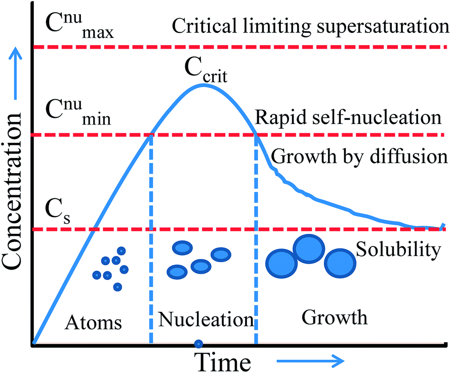
Thus, wet-chemical methods involve nucleation and growth processes during the formation of metal NPs, which are summarized in Fig. 7 based on the LaMer and Dinegar model.109 In the initial stage, the decomposition of the precursor takes place, and hence the concentration of metal ions steadily increases. Once, the concentration reaches the stage of supersaturation (Cs) then nucleation takes place. However, nuclei formation starts only when the concentration of the metal atoms reaches a critical concentration (Ccrit). As the nuclei grow, the concentration of metal ions in solution drops, and when the concentration of metal ions drops below the level of supersaturation, then nucleation stops. Therefore, the continuous supply of metal ions is necessary to grow the nuclei into nanocrystals. Thus, nucleation and growth can be engineered for size and shape-controlled synthesis of metal NPs. Meanwhile, it is unclear from this model whether metal ions are reducing before the nucleation or vice versa. This would need further investigation for being clarified.
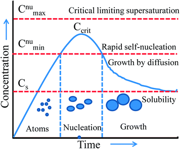 |
| | Fig. 7 LaMer model describing nucleation and growth of nanocrystals as a function of reaction time and concentration of precursor atoms. Reprinted with permission from ref. 109. Copyright 1950 American Chemical Society. | |
It is important to note that bare metal NPs are unstable in solution, and hence stabilizing agents are used. The electrostatic and steric stabilization are the two ways by which stabilizing agents stabilize metal NPs in solution.110 In electrostatic stabilization, both double layer repulsion and van der Waals attraction are involved, whereas in steric stabilization van der Waals and steric forces are involved. In steric stabilization, the aggregation of NPs is prevented by the adsorption of large capping molecules (e.g. polymers or surfactants). Furthermore, the colloidal stability is also affected by particle size; therefore nanosized and micron-sized particles require different mechanisms to achieve colloid stability.
3.2 Noble metal@metal oxide core–shell NPs
The size and shape-dependent properties of noble metal NPs can be retained only when they are protected against coalescence. However, electrostatic or steric stabilization of metal NPs in colloids becomes ineffective against coalescence when the colloids are exposed to severe conditions. For example, the DSSC fabrication process involves transfer of metallic NPs from the colloidal phase to the powder phase followed by sintering at ∼500 °C. Therefore, the core–shell geometry in which noble metals present in the core are protected with a shell for their stability can be a good approach for addressing this issue.111,112 For example, gold and silver colloids are often protected by coating with different materials such as SiO2, TiO2, etc.26–28,113,114 The formation of metal@semiconductor core–shell NPs also generates unique optical, electronic or magnetic properties.26–28,113,114 Thus, the optical properties of these core–shell colloids can be tuned by tuning the shape, size and composition of either the core or the shell or both. Since, plasmonic core–shell NPs used in DSSCs mainly involve either Ag or Au as the plasmonic core and SiO2 or TiO2 or both as the metal oxide shell. Therefore, recent advances in the synthesis and properties of these core–shell NPs are discussed in this section.
3.2.1 Metal@SiO2 core@shell NPs.
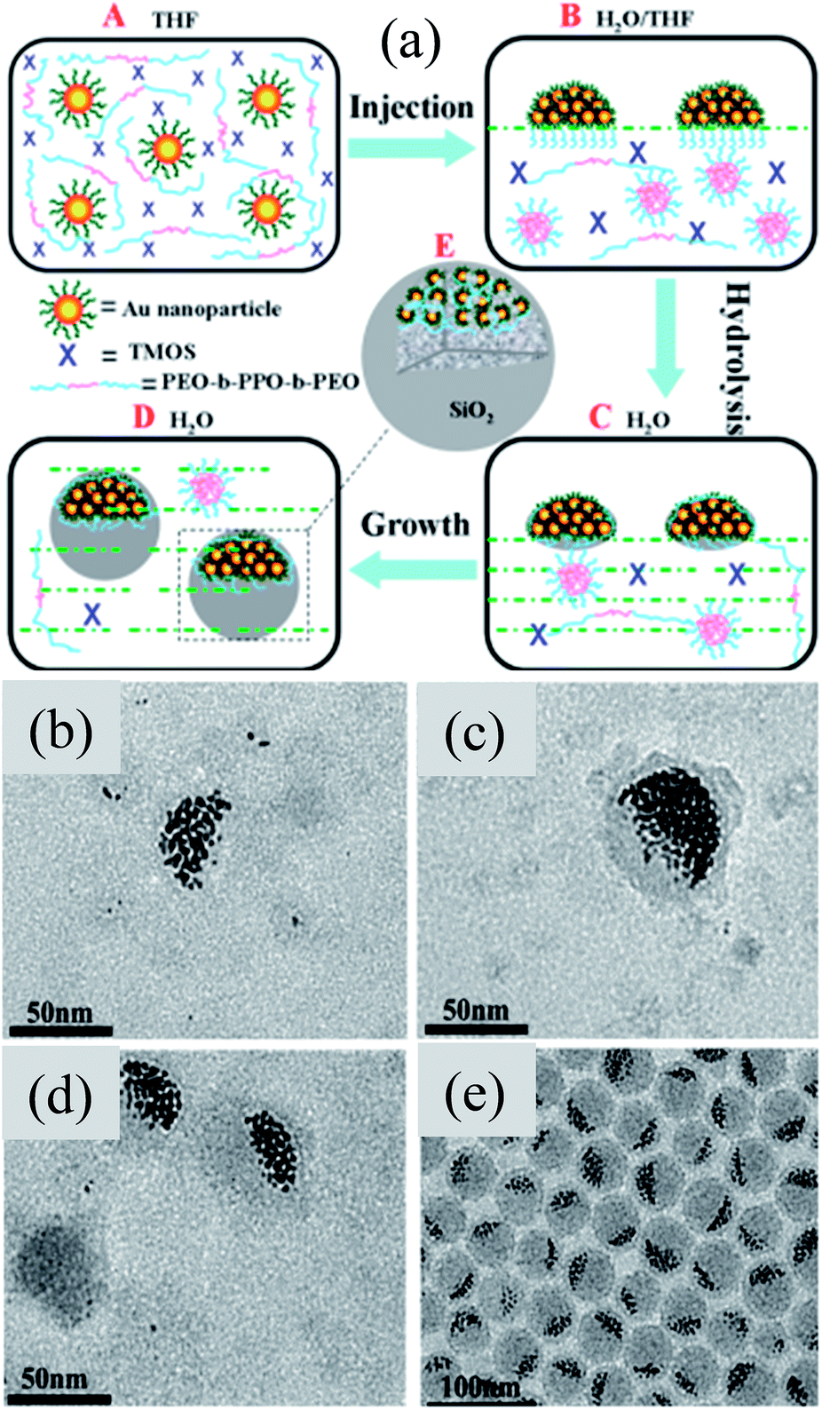
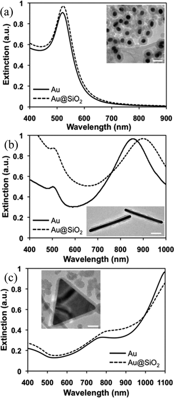
SiO2 is highly stable against coagulation and hence it is widely used as a shell material.115–117 Apart from this, silica coating is highly practiced due to its optical transparency, chemical inertness, thermal stability, low cost and simple methodology.118 Patil et al. synthesized Au@SiO2 and Ag@SiO2 clusters with a controlled composition and size by means of gas phase annealing at extremely high temperatures (∼1500 °C).119 Pioneering work in the field of wet-chemical silica coating of noble metals was carried out by Liz-Marzán, Mulvaney, and co-workers.120–127 In these methods, mostly (3-aminopropyl) trimethoxysilane (APS) was used as a coupling agent to make the surface of noble metals compatible with silicate moieties. The deposition of SiO2 shells on noble metals was carried out by the Stober method.128 However, silica deposition by the Stober method suffers from the dissolution of the Ag cores due to the presence of concentrated ammonia. Therefore, Xia and co-workers developed a poly-ol method where noble metals have been directly coated with a silica shell without using any primer.129,130 Since, anisotropic NPs are of great importance due to their unique physical properties, much effort has been focused on the synthesis of non-spherical NPs, such as nanorods,131–134 triangular prisms,137–140etc. However, coating of anisotropic metal NPs with SiO2 was challenging via the Stöber method. Therefore, various synthesis techniques are used for the synthesis of anisotropic M@SiO2 core–shell NPs.131–136 However, these techniques require several surface functionalization steps and yield M@SiO2 core–shell NPs with thick (∼30–70 nm) silica shells.
Recently, Wei and co-workers have presented a versatile method for the synthesis of anisotropic Au@SiO2 core–shell nanostructures with a controllable silica shell thickness.137 They found that the cetyltrimethylammonium bromide (CTAB) concentration and Au NP number density played an important role in shell formation and optimized them for control over the shell thickness (5–20 nm) without forming any free silica NPs. The formation of a silica shell resulted in a red-shift of the SPR band of Au NPs due to an increase in the refractive index (Fig. 8). Furthermore, the change of shape from spherical to non-spherical resulted in an extensive red-shift with multiple peaks depending on the shapes as displayed in Fig. 8.
 |
| | Fig. 8 Vis-NIR spectra and TEM images (insets) of Au@SiO2 core–shell (a) nanospheres, (b) nanorods, (c) nanoprisms. All scale bars are 50 nm. Reprinted with permission from ref. 135. Copyright 2012 Royal Society of Chemistry. | |
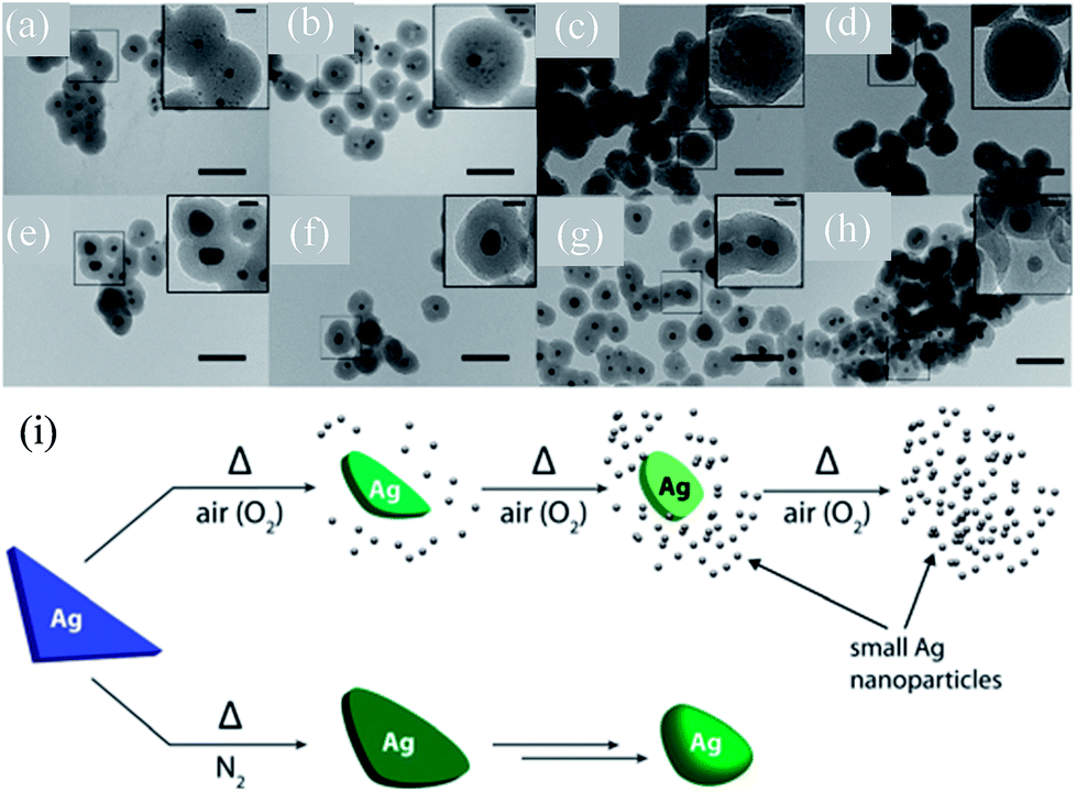
Gangishetty et al. synthesized triangular Ag@SiO2 core–shell NPs and studied the effect of thermal annealing on the shape, size, composition, and LSPR of noble metal NPs.138–140 It was found that the plasmon band of the Ag@SiO2 nanotriangles was drastically blue-shifted (720 to 420) when annealed in air.138 In contrast, the samples annealed in a N2 atmosphere have shown a moderate blue-shift (720 to 660 nm) upon annealing at 150 °C, which further blue-shifted upon annealing at higher temperatures. It is interesting to note that an additional peak at 440 nm also appeared in the spectra of all post-annealed samples. Gangishetty et al. postulated that annealing in air resulted in the oxidation and detachment of vertices of the Ag@SiO2 nanotriangles in the form of AgxO. Meanwhile, the dissociated AgxO decomposes back into small Ag NPs around the remaining Ag core (Fig. 9a–d). It has been found that at higher temperatures, such as 600 °C, the entire Ag core fragmented into smaller NPs. However, annealing in a N2 atmosphere resulted only in rounding of the Ag nanotriangles without fragmentation (Fig. 9e–h). Thus, the large blue-shift in the air annealed sample is associated with fragmentation, whereas the small shift in the N2 environment is associated with rounding of vertices of Ag NPs.
 |
| | Fig. 9 TEM images of the Ag@SiO2 nanotriangles after annealing in either (a–d) air or (e–h) N2 atmospheres and (i) proposed thermal degradation mechanism. The samples were annealed at: (a and e) 150 °C, (b and f) 300 °C, (c and g) 450 °C, and (d and h) 600 °C. The scale bars in the main images are 100 nm, while those in the insets are 20 nm. Reprinted with permission from ref. 140. Copyright 2016 Royal Society of Chemistry. | |
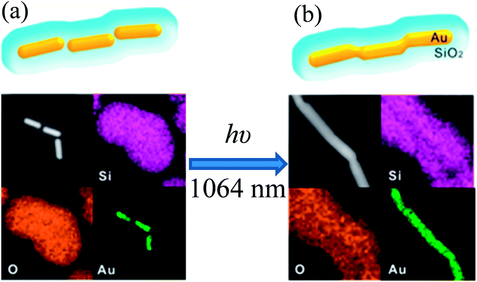
In an interesting study, Son et al. reported a unique technique to fabricate one dimensional Au@SiO2 core–shell nanowires via nanowelding of a silica-coated Au nanorod chain by laser irradiation as depicted in Fig. 10.141 First, Au nanorod chains are formed via self-assembly of Au nanorods in an end-to-end orientation without using any assembling agents. It has been found that CTAB, used for the synthesis of Au nanorods, has played a critical role in the formation of the Au nanorod chain and its colloidal stability. Since, CTAB forms only a monolayer at the tip of Au nanorods due to its small curvature as compared to the bilayer on the sides. Thus, CTAB tends to form a bilayer on the tip of Au nanorods to provide colloidal stability, and hence Au nanorod chains are formed via end-to-end self-assembly. The silica-coated Au nanochains were synthesized by directly coating the Au nanorod chain. Au nanorods in a silica-coated gold nanochain have maintained their original shape and they were separated from each other by a distance of 8 nm due to the presence of the CTAB bilayer (Fig. 10a). The assembly of Au nanorods into a chain-like structure resulted in a decrease of the longitudinal SPR band of individual gold NRs at 830 nm and a new SPR band arises beyond 1000 nm for Au nanochains. The red-shift in the SPR band after chain formation is basically related to the coupling of the longitudinal SPR band of linearly assembled gold NRs. Finally, silica-coated Au nanowires were fabricated by laser irradiation, where laser pulses were selectively absorbed by the SPR of linearly assembled Au nanorods in silica shells and fused together (Fig. 10b). These results demonstrate that laser pulses have selectively heated the contacting surfaces of the Au nanorods, which resulted in the fusion of Au nanorods to form Au nanowires.
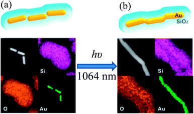 |
| | Fig. 10 TEM images and corresponding EDX elemental maps of (a) a SiO2-coated Au nanochain (before irradiation) and (b) a SiO2 coated Au nanowire (after irradiation). Reprinted with permission from ref. 141. Copyright 2014 American Chemical Society. | |
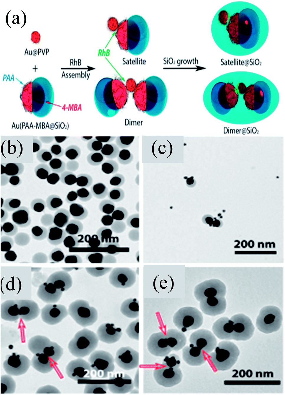
Chen et al. developed an approach for the selective deposition of SiO2 on Au NPs to form an Au@SiO2 Janus structure.142 They found that a Au@SiO2 core–shell structure was formed when 4-mercaptophenylacetic acid (4-MPAA) was employed as the only ligand and it was not formed when poly-(acrylic acid) (PAA86) was used as the sole ligand. However, when both of these ligands were used, then Janus Au@SiO2 NPs were formed. This phenomenon can be explained on the basis of competitive ligand co-ordination of 4-MPAA and PAA, where a partial surface of Au NPs was functionalized by 4-MPAA and others by PAA. Thus, a SiO2 layer was deposited on the 4-MPAA side of Au NPs only leading to the formation of Janus-like structures. In a similar study, Liz-Marzan and co-workers reported the formation of self-assembled Janus NPs guided by van der Waals forces and electrostatic attraction between PVP and PAA at low pH (Fig. 11a).143 These Janus Au@SiO2 dimers were then sealed with a second SiO2 shell in order to prevent the dissolution of the first semi-SiO2 shell of Janus NPs. TEM images clearly show the presence of Janus NPs and their self-assembly to form the dimers (Fig. 11b and c). SiO2 coating of dimers clearly shows two Janus particles linked by small Au spheres and some silica nucleation (Fig. 11d and e). Similarly, self-assembly of Au@SiO2 Janus NPs was also carried out by addition of a hydrophobic thiol which was selectively grafted on the gold moiety.144 Liz-Marzan and co-workers prepared Au@SiO2 Janus nanostars, where Au spikes were grown on the uncoated side of Au NPs using L-ascorbic acid in the presence of AgNO3 and HCl (aq).145 They found that spikes can only be grown in the presence of silver ions, otherwise, metal overgrowth takes place without branch formation.
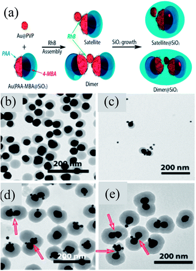 |
| | Fig. 11 (a) Rhodamine B isothiocyanate (RhB) incubated with Au15@PVP spheres and Janus Au40(PAA-MBA@SiO2) particles. Representative TEM images: (b) Au40(PAA-MBA@SiO2) Janus particles; (c) intermediate structures formed after 5 min of assembly; (d and e) Au–SiO2 hybrid satellites. Red arrows indicate the position of Au15 acting as a linker for the Janus particles. Reprinted with permission from ref. 143. Copyright 2015 American Chemical Society. | |
Instead of conventional Janus Au@SiO2 nanostructures, Li et al. synthesized Janus Au@SiO2 NPs with a number of Au NP off-centers as shown in Fig. 12a.146 It has been found that the Au NPs (3 nm) are hydrophobic in nature and formed a hemisphere in water due to aggregation in order to lower the hydrophobic–hydrophilic interfacial energy (Fig. 12b and c). It is important to note that these Au NP hemispheres exhibit a weak affinity toward SiO2; therefore the block copolymer Pluronic F127 was used as a primer for SiO2 coating. These Au@SiO2 clusters have a uniform shape and size (∼40 nm), where each contains a hemisphere consisting of a number of aggregated Au NPs on one side of the cluster (Fig. 12d). An important result is that the position of the SPR peak (∼500 nm) remained unchanged for the as-synthesized 3 nm Au NPs and for Au-SiO2 asymmetric clusters, suggesting that the aggregated Au NPs are individually dispersed in the Au–SiO2 asymmetric clusters. However, a red-shift of 30 nm was observed when Au@SiO2 clusters were annealed at 400 °C due to the change in the refractive index of the surface layer.
 |
| | Fig. 12 (a) Scheme showing the formation of Au–SiO2 asymmetric clusters by a modified Stöber method. TEM images showing the as-synthesized Au–SiO2 asymmetric clusters at different stages of reaction time: (b) 8, (c) 24, (d) 48, and (e) 96 h. Reprinted with permission from ref. 146. Copyright 2013 American Chemical Society. | |
As an alternative to core–shell nanostructures, Song and co-workers synthesized Au@SiO2 yolk–shell NPs (having an air void in between the core and shell) via selective etching of the Au core in Au@SiO2 core–shell NPs.147,148 However, the high toxicity of KCN has limited the wider application of this approach. Recently, hot water was used as the etching agent to synthesize Au@SiO2 yolk–shell.149,150 The yolk–shell formation mechanism suggests that SiO2 layers are inhomogeneous in nature, where the outer SiO2 layer is chemically more robust than the inner layer. Therefore, inner SiO2 layers were selectively etched with hot water to form yolk–shell structures. Furthermore, aging time and storage conditions of core–shell NPs are also very important, as chemicals present in colloids can result in the formation of yolk–shell nanostructures.151 Guo et al. developed a novel strategy to synthesize Au@SiO2 yolk–shell by hydrothermal treatment in the presence of compressed CO2, without using an etching agent.152 Since CO2 induces the formation and swelling of the micelle structure, the usage of a traditional swelling agent is avoided. Liu et al. synthesized Ag@SiO2 yolk–shell NPs by a “two solvents” impregnation method.153 Apart from the single core, multi-core Ag@SiO2 yolk–shell NPs with different numbers of Ag NPs were prepared via selective etching methods.154 In this approach, at first multiple Ag NPs embedded in a SiO2 matrix were prepared. These hybrid Ag@SiO2 NPs were further coated with a second SiO2 layer. Finally, the interior silica was selectively etched at controlled pH and, therefore, multiple Ag NP-loaded hollow SiO2 NPs are formed.
3.2.2 Metal@TiO2 core@shell NPs.
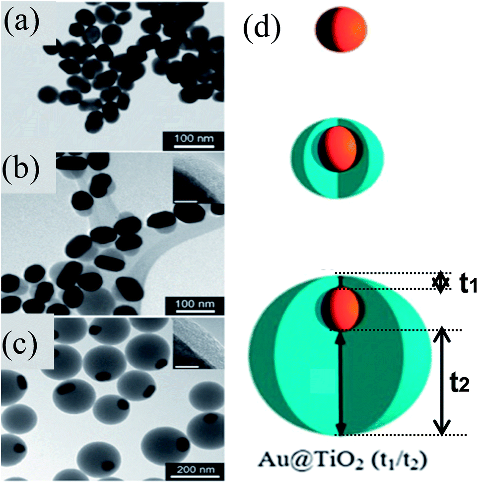
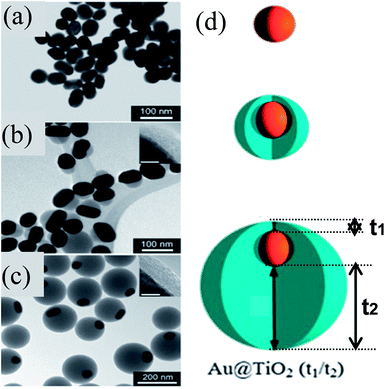
Similar to M@SiO2 core–shell, M@TiO2 core–shell NPs have also been extensively investigated for DSSC applications. M@TiO2 core–shell NPs are also synthesized by similar sol–gel methods to those used for the synthesis of M@SiO2 core–shell.155–164 Mostly concentric core@shell NPs are synthesized by sol–gel methods; however, Han and co-workers synthesized eccentric Au@TiO2 core@shell NPs via a sol–gel method as shown in Fig. 13a–c.165 They found that citrate ions used for the reduction and stabilization of Au NPs have strongly bound to the (111) plane as compared to the (110) and (200) planes of Au NPs. The formation of eccentric core@shell NPs involved plane-selective condensation of TiO2 onto citrate-capped Au NPs, where the TiO2 precursor has selectively displaced the weakly bound citrate ions from (110) and (200) planes. It is important to note that the thickness of TiO2 remains constant on the strongly bound citrate side (5 nm) and increased from 25 to 125 nm on the weakly bound citrate side (Fig. 13b–d).
 |
| | Fig. 13 (a–c) TEM images of (a) 50 nm Au cores, (b) Au@TiO2 (5/25) and (c) Au@TiO2 (5/125) nanostructures. The thinner sides of the TiO2 shells are shown (insets) for (b) and (c). Scale bars of inset = 5 nm. (d) Schematic of shell formation. Reprinted with permission from ref. 165. Copyright 2011 Royal Society of Chemistry. | |
Recently, the hydrothermal method has been found to be a useful technique to synthesize well-defined concentric M@TiO2 core–shell NPs with high crystallinity.166,167 First, Li et al. used the hydrothermal method to deposit a TiO2 shell (200–500 nm) on a pre-formed Au NP core (50–150 nm) to form Au@TiO2 (500–800 nm) core–shell NPs (Fig. 14a). This is a two-step process where the shape and size of the core as well as shell can be easily controlled by controlling the reaction parameters, such as time, temperature, concentration, etc. Aging of Au@TiO2 core–shell NPs resulted in the formation of a yolk–shell structure via Ostwald ripening (Fig. 14b). The hollow space between the core and shell in these yolk–shell NPs was minimized via soaking them in a HAuCl4 solution through the reduction of gold ions (Fig. 14c). TiO2 shells produced through hydrothermal methods are crystalline in nature and their shape and size can be easily controlled. Therefore, this approach was practiced by many researchers to produce core–shell NPs with different metal cores and shell thickness. It has been found that microwave heating instead of conventional heating during the hydrothermal reaction has significantly reduced the preparation time for M@TiO2 core–shell NPs.64,168 The phase transition (anatase to rutile) of TiO2 in Au@TiO2 core–shell NPs was also restricted up to 900 °C in the presence of air as compared to ∼550 °C for bare TiO2 NPs. It was proposed that the formation of Ti–O–Au bonds at the interface of Au@TiO2 core–shell was responsible for the stability of the anatase phase. Furthermore, the shape and size of Au@TiO2 core–shell NPs remained unchanged except for an increase in the crystallinity of TiO2 with calcination temperature.
 |
| | Fig. 14 (a) Schematic illustration of Au@TiO2 nanoreactor formation and size tuning of the core catalyst, (b) TEM images of Au@TiO2 core@shell nanoreactors with a central vacant space (prepared in step 3 of (a)), and (c) after enlargement of Au cores (prepared in step 4 of (a)). Reprinted with permission from ref. 166. Copyright 2005 Wiley-VCH. | |
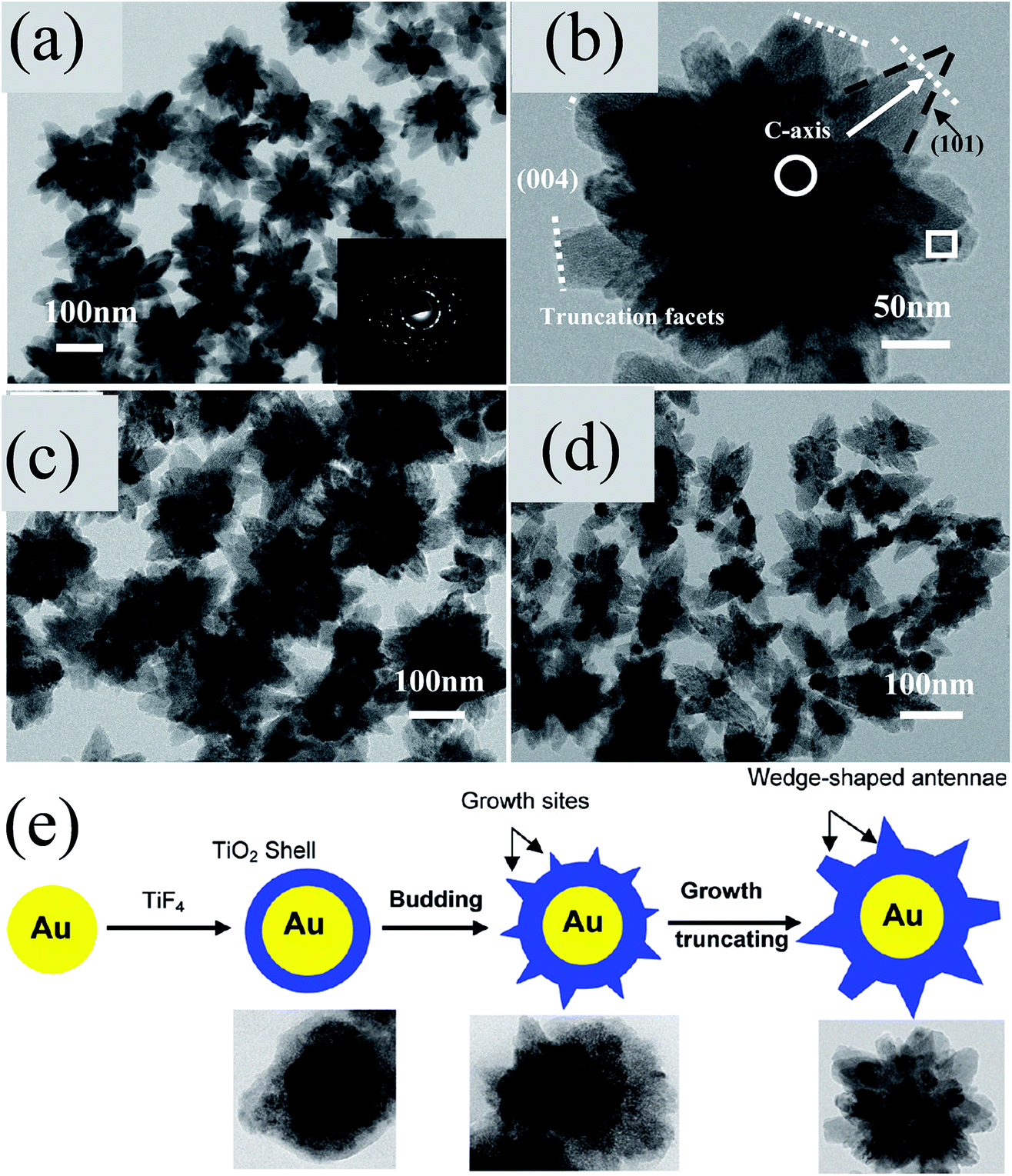
As compared to spherical shells with uniform thickness reported earlier, Wu et al. prepared M@TiO2 core–shell NPs with truncated wedge-shaped TiO2 shells as shown in Fig. 15a–d.169,170 They proposed that the wedge-like structure was formed due to epitaxial growth with segmented orientation, where F− ion concentration (produced from hydrolyzed TiF4 precursors) played an important role (Fig. 15e).169 In the core region (Au–TiO2 interface), TiO2 grew epitaxially along (101) crystal planes to minimize the interfacial energy due to lattice matching with exposed Au (111) planes. However, in the rim region the growth direction changed from the (101) to the (001) plane, and thus the antenna preferentially grew along the [001] direction (Fig. 15e).
 |
| | Fig. 15 TEM images of the as-prepared (a) Au@TiO2 core@shell NPs and (b) individual particle image, (c) Ag@TiO2 NPs, (d) Pt@TiO2 NPs, and (e) schematic diagram of the proposed formation process of Au@TiO2 core@shell NPs with a truncated wedge-shaped morphology. Reprinted with permission from ref. 169. Copyright 2009 American Chemical Society. | |
The change in solvent from water to alcohol resulted in the formation of hollow Au@TiO2 core@shell NPs through Ostwald ripening.171,172 Multicore M@TiO2 core–shell NPs were also prepared by the hydrothermal method.173,174 For example, Ag@TiO2 core–shell NPs with multiple Ag NPs as cores were synthesized and employed as a catalyst for the reduction of 4-nitrophenol (4-NP).174 It was found that multiple Ag cores provide more active sites for catalysis as compared to traditional metal@TiO2 core–shell NPs. The hydrothermal method was also used to synthesize anisotropic M@TiO2 core–shell, such as Ag@TiO2 core–shell nanowires by using Ag nanowires as templates.175–177 Meanwhile, Du et al. synthesized Ag@TiO2 core–shell nanowires via a one-step polyol method without using a template.178 In an interesting study, Sahu et al. synthesized Au@TiO2 nanowires, where TiO2 nanotubes were first grown in alumina templates using a sol–gel method followed by growth of gold nanowires in the pores of these tubes by electrodeposition.179 However, the polycrystalline nature of the metal resulted in a poor contact between the oxide and the metal and through the metal core.
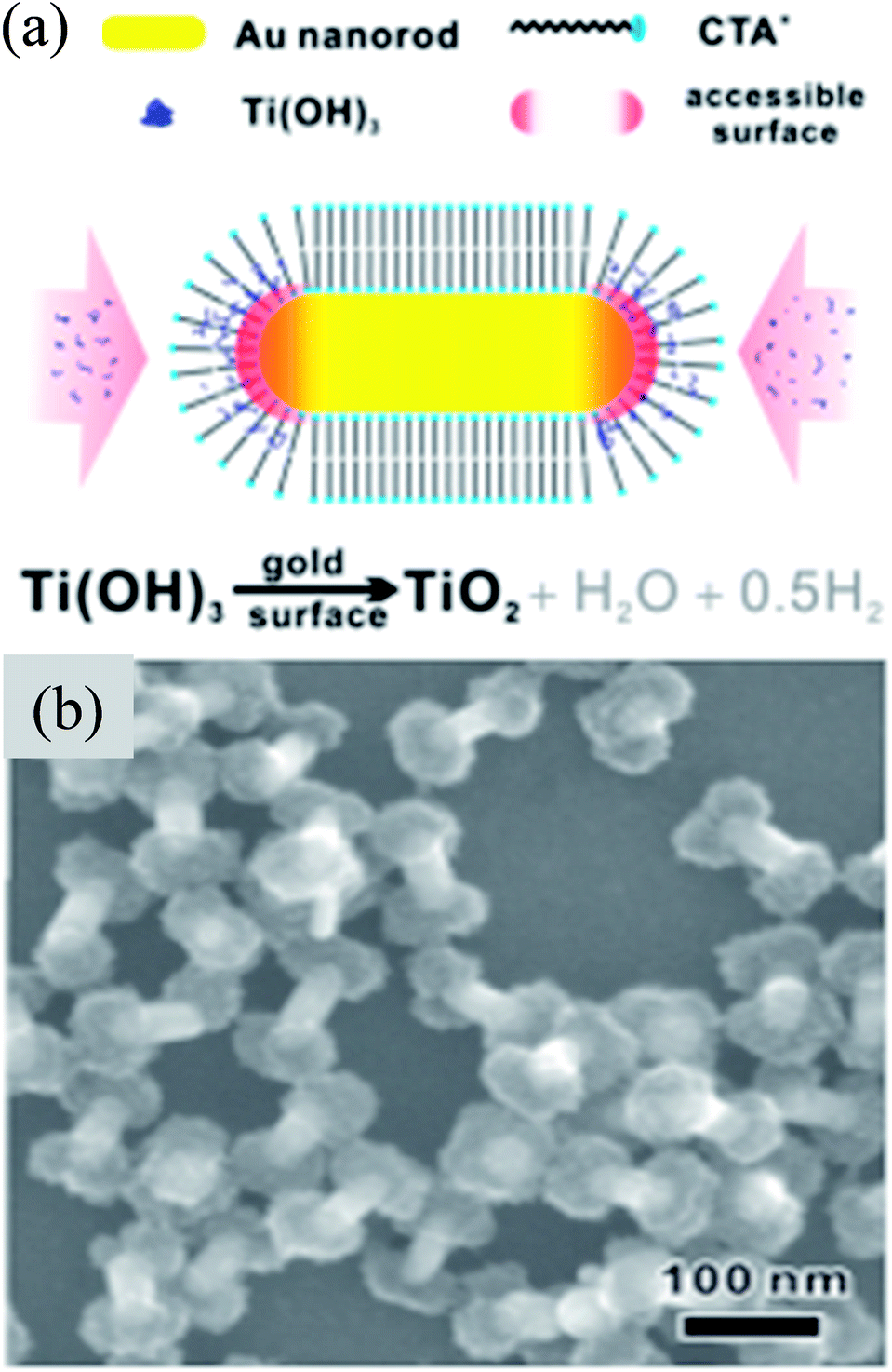
Recently, Wu et al. have synthesized uniform dumbbell shaped Au@TiO2 core–shell NPs, where TiO2 NPs were deposited only on the tips of Au nanorods using CTAB as a soft template (Fig. 16).180 These TiO2 caps are made of 2 nm building block units and porous in nature. The assembly of CTAB on the tips is less compact due to curvature as compared to sides of Au nanorods. Therefore, deposition of TiO2 on the tips of Au nanorods was easier due to lower electrostatic repulsion between positively charged CTAB and Ti+4 cations. The deposition of TiO2 decreased from thicker to thinner nanorods due to a reduced area for nucleation and growth on the tips. The formation of TiO2 caps on the tips of Au nanorods resulted in a red-shift of SPR bands due to the change in the local refractive index.
 |
| | Fig. 16 (a) Schematic showing the origin of anisotropic TiO2 coating. (b) SEM image of the as-prepared Au nanorods@TiO2 nanodumbbells. Synthetic conditions: 32 nm Au NRs (in diameter), 13.9 mM C16TAB. Reprinted with permission from ref. 180. Copyright 2016 American Chemical Society. | |
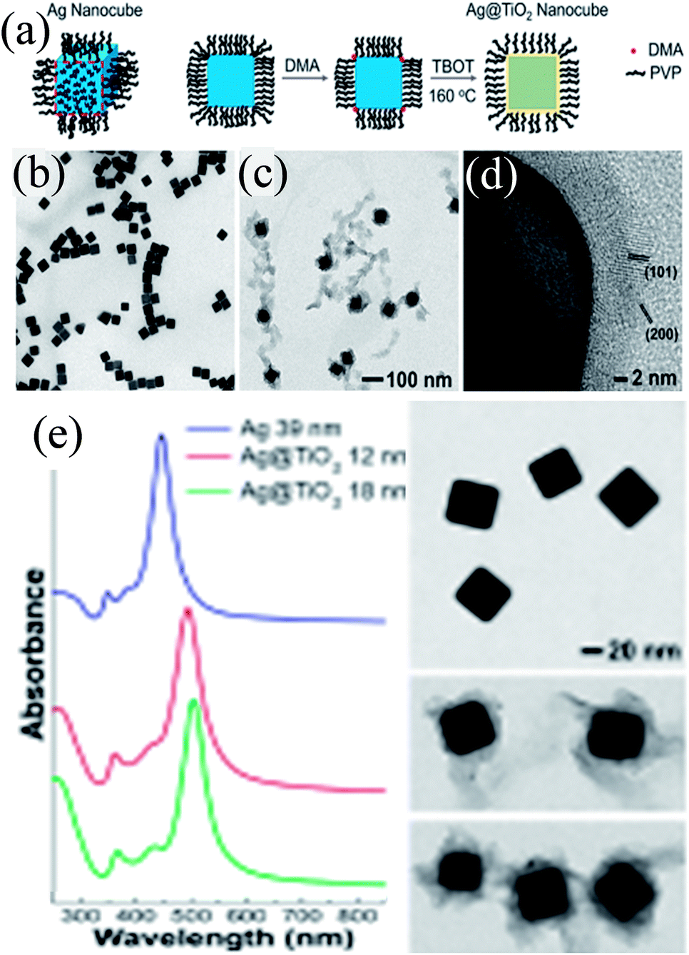
Peckus et al. synthesized cubic Ag@TiO2 core–shell NPs in a two step process, where Ag nanocubes were synthesized by the poly-ol method in the first step and coated with a TiO2 shell in the second step using amine as the hydrolyzing agent (Fig. 17a).181 The cubic shape and size (edge length 39 ± 3 nm) of the Ag nanocube were maintained during shell formation (Fig. 17b–d). It was found that amine, a gentle base, hydrolyzed TiO2 precursors without etching Ag nanocubes. The thickness of the TiO2 shell was not uniform (8–16 nm) and free TiO2 NPs could also be found in TEM images, suggesting higher difficulties in coating a cubic structure than a spherical one (Fig. 17c and d). The SPR band of Ag nanocubes red-shifted (47 nm) after the formation of a 12 nm TiO2 shell and further shifted as the shell thickness was increased (Fig. 17e).
 |
| | Fig. 17 (a) Illustration showing the procedure for conformally coating Ag nanocubes with TiO2 shells (DMA = dimethylamine, TBOT = tetra-n-butyl orthotitanate, and PVP = polyvinylpyrrolidone). TEM images show a dispersion of (b) Ag nanocubes (a = 39 nm) and (c) Ag@TiO2 nanocubes using the same magnification. (d) HRTEM micrograph of the TiO2 shell showing that it is polycrystalline and in intimate contact with the Ag nanocube. The lattice spacings match the {101} and {200} planes of anatase phase TiO2. (e) Steady-state UV-VIS absorption spectra of Ag and Ag@TiO2 nanocubes. TEM images of the nanocubes are to the right of their corresponding spectra. Reprinted with permission from ref. 181. Copyright 2017 American Chemical Society. | |
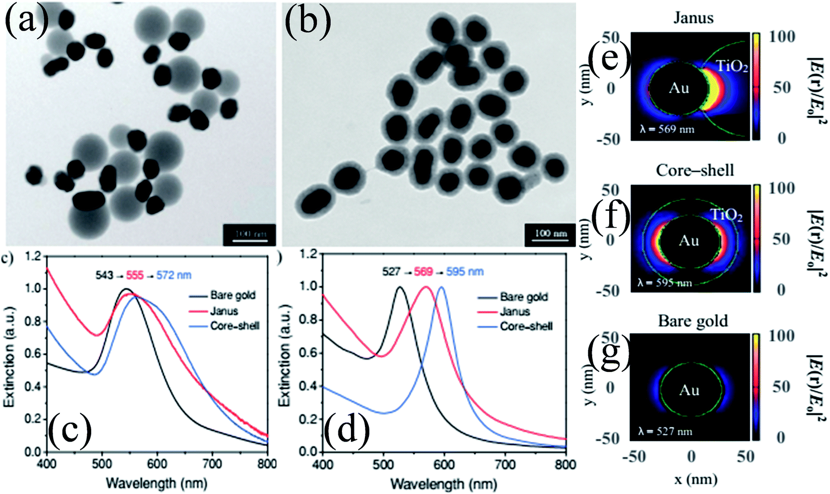
As compared to concentric M@TiO2, eccentric M@TiO2 core–shell NPs have also been synthesized by various researchers.182,183 For example, She et al. synthesized Au@TiO2 core–shell and Janus NPs and investigated the morphological effect on optical and photocatalytic properties.182 It is important to note that the size of Au NPs was the same in both samples and an equal amount of TiO2 precursor was used. TEM images show that Au NPs were uniformly coated with a TiO2 shell in core–shell structures, whereas it was deposited on one side of Au NPs in Janus-like structures (Fig. 18a and b). UV-visible absorption spectra show a red-shift in the SPR band of both structures as compared to Au NPs due to the increase in the refractive index of the medium (Fig. 18c). However, the shift in the SPR band for core–shell structures was slightly higher than that of Janus NPs mainly because Au NPs were coated with TiO2 on all sides in core–shell structures. The asymmetric structures of Janus NPs also resulted in asymmetric localization of the plasmonic near-fields, i.e. only on one side of the Au NPs (Fig. 18e) as compared to symmetric localization in core–shell NPs (Fig. 18f). Since Janus NPs are surrounded by TiO2 on one side and isopropanol on the other side, there is a big dielectric mismatch which resulted in preferential localization of the plasmonic near-fields close to the Au–TiO2 interface.
 |
| | Fig. 18 TEM images of (a) Janus and (b) core–shell Au 50 nm@TiO2 nanostructures. (c) Optical-extinction spectra of bare gold NPs (50 nm), as well as Janus and core–shell Au 50 nm-TiO2 nanostructures in isopropyl alcohol, which were derived from experimental measurements and (d) DDA simulations. Plasmonic near-field maps (cross-sectional view at z = 0) simulated using DDA for (e) Janus Au 50 nm-TiO2, (f) core–shell Au 50 nm-TiO2 and (g) bare gold nanoparticles (50 nm). The maps show the electric near-field intensity enhancements |E(r)/E0|2 of the nanostructures at their LSPR wavelengths (indicated on each map) with the incident polarization along the x-axis. Reprinted with permission from ref. 182. Copyright 2012 Wiley-VCH. | |
Furthermore, M@TiO2 yolk–shell NPs were synthesized by a template method, where a sacrificial layer of silica or carbon was used to form an air void. The size of the void space inside the TiO2 shells was controlled by the size of the template.184–189 For example, Shi et al. synthesized monodispersed Au@TiO2 yolk–shell nanospheres using SiO2 as a sacrificial template and these nanospheres were used as building blocks for 3 dimensional arrays of Au@TiO2 (3D-array).190 Here, Au NPs were coated with two layers of SiO2, where one layer was used as a sacrificial layer for void creation and other is used as a protector to form a 3D-array of Au@TiO2 NPs (Fig. 19 a). Thus, Au@TiO2 yolk–shell NPs were uniformly synthesized via the SiO2 protection method, where a cavity of 176 nm in diameter was formed in between the core and shell (Fig. 19b–f). It is interesting to note that the SPR band of Au NPs initially located at 530 nm was red-shifted to 547 nm after coating of the SiO2 first layer; however no shift is observed for TiO2 and the second layer of SiO2 coating. When both SiO2 layers were removed, then the SPR band was slightly blue-shifted to 541 nm. It has been found that 3D-arrays of Au@TiO2 exhibited a much higher photocatalytic activity as compared to Au@TiO2 NPs mainly because of the elongation of the light path length due to the multiscattering in-between Au–TiO2 and the reflection inside of the TiO2 shell (Fig. 19c). Therefore, the Au NPs in 3D arrays can absorb more solar light and can generate more hot-electrons through the electron transfer from Au NPs to the TiO2 shell.
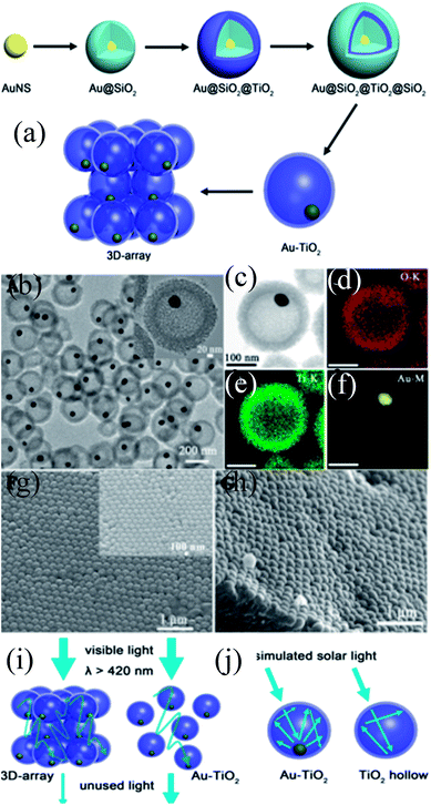 |
| | Fig. 19 (a) Schematic illustration of synthesizing Au–TiO2 and 3D arrays, (b) TEM image of Au–TiO2, inset image shows the enlarged Au–TiO2, (c) HAADF-STEM image of Au–TiO2, (d) elemental mappings of O, (e) Ti and (f) Au, (g) SEM images of the 3D-array, inset is the enlarged image, (h) intersection image of the 3D-array, (i) Schematic illustration of the enhanced photocatalytic activity of the 3D-array compared with Au–TiO2 under visible light irradiation and (j) solar light irradiation. Reprinted with permission from ref. 190. Copyright 2016 American Chemical Society. | |
4. Application of plasmonic noble metal@metal oxide core–shell NPs in DSSCs
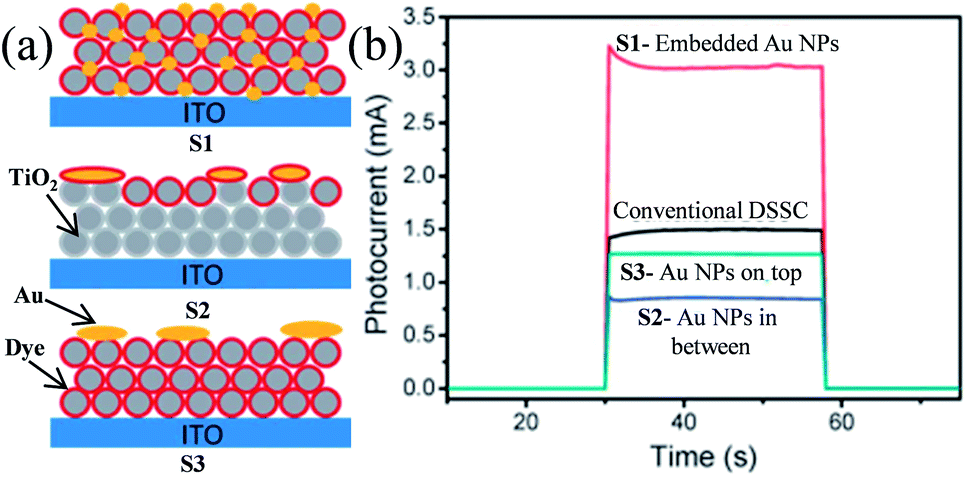
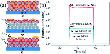
Plasmonic NPs show two characteristic properties when they interact with visible light. First, they show an intense absorption feature at particular wavelengths of light which are resonant with their electron oscillation. Second, plasmonic NPs can greatly enhance the electromagnetic field near the surface. Thus, plasmonic NPs have been used as absorption amplifiers in DSSCs to improve their efficiency.19–23 However, commonly used redox electrolytes in DSSCs include I−/I3− ions, which are extremely corrosive toward Ag and Au NPs.23–25 Therefore, protection of plasmonic NPs along with maintaining the electromagnetic coupling between the plasmonic NPs and the dye is very important for DSSC application. Therefore, Hupp and co-workers coated Ag NPs with a TiO2 shell of different thicknesses using atomic layer deposition to protect the Ag NPs from corrosive I−/I3− based electrolytes.191 They found that a minimum 7.7 nm thick TiO2 shell is required to protect the Ag NPs from corrosion. Based on this result, they also examined the distance dependence of the plasmon-enhanced properties in DSSCs using Ag NPs on a TiO2 film.192 They found that the TiO2 based electrode with only Ag NPs and without dye produced no significant current, whereas cells having the dye only showed a conversion efficiency of ∼0.2%. In contrast, cells comprising both Ag NPs and dye showed ∼1.4% conversion efficiency. However, the efficiency decreases with increasing TiO2 shell thickness due to the decay in the electromagnetic field with an increase in the distance between dye and plasmonic NPs. This decay in the electromagnetic field resulted in a decrease in the plasmon-enhanced extinction of the dye. Furthermore, with an increase in shell thickness, the SPR band red-shifted, and hence the spectral overlap between the plasmon and the dye weakened, which also resulted in decreased efficiency. Thus, the combined results of these two effects are responsible for lower plasmon-enhanced dye extinction in thicker TiO2 shells. They also found that amorphous TiO2 exhibited higher efficiency than anatase TiO2 of the same thickness. Thus, from this study it is clear that maximum plasmon enhancement in efficiency of DSSCs can only be achieved when the thinnest and pin-hole free TiO2 shell can be developed. In contrast, Ding et al. reported that the corrosion of Ag NPs can be significantly prevented by N-719 dye loading on Ag NPs, as iodide ions exchange electrons with the dye rather than the Ag layer.193 The efficiency was increased from 2.7% to 4.0%, with the addition of 22 vol% of Ag coated SiO2 core–shell NPs into the TiO2 based photoanode. In a similar study, Hou et al. found that the position of plasmonic NPs in the working electrode also plays an important role in the improvement of efficiency in DSSCs.194 They fabricated three kinds of working electrodes where S1 is a monolayer of Ru dye N719 deposited on top of Au NPs embedded in a TiO2 film, S2 is a monolayer of Ru dye N719 on top of an evaporated 5 nm Au-island thin film deposited on the TiO2 layer, and S3 is an evaporated 5 nm Au-island thin film deposited on top of the dye monolayer and the TiO2 layer (Fig. 20a). Among these three cells, the cell S1 provided the highest efficiency of 2.28% which was 2.4 times higher than that of conventional DSSCs i.e. without Au NPs (0.94%). The enhancement in efficiency was related to the intense local electromagnetic fields produced by the Au NPs, which coupled with light very effectively from the far-field to the near-field of the dye (spectral overlap). It is interesting to note that photocurrents produced by cells S2 and S3 are lower than that of conventional DSSCs. This decrease in efficiency is either related to the reduced effective area of TiO2 in contact with the dye molecules (cell S2) or the decreased dye area exposed to the light by the Au NP layer (cell S3). Furthermore, no photocurrent was observed for bare TiO2 and Au NPs embedded in the TiO2 electrode in the absence of the dye molecule. This result is of great importance and confirms that the plasmon excited electrons cannot be transferred directly from the Au NPs to the TiO2 in DSSCs.
 |
| | Fig. 20 (a) Schematic diagrams of three different Au NPs/dye/TiO2 configurations. (b) Short-circuit photocurrents of DSSCs with three different Au NPs/dye/TiO2 configurations. Reprinted with permission from ref. 194. Copyright 2011 Royal Society of Chemistry. | |
4.1 Effect of core–shell NPs
In a succeeding study, it was found that the dye loading on metal NPs is an ineffective barrier for metal corrosion. Furthermore, bare metal NPs in DSSCs act as charge recombination centres. Therefore, incorporation of bare metal NPs in DSSCs is detrimental due to these two reasons.195 For example, Brown et al. added bare plasmonic NPs into a photoanode and light absorption monotonically increased with increasing amounts of plasmonic NPs.196 However, the photocurrent, photovoltage and fill factor of both solid-state and liquid electrolyte based DSSCs monotonically decreased due to internal short-circuits. This internal short-circuit resulted from plasmonic NPs which were acting as recombination centers within the device. In contrast, when plasmonic NPs with a thin shell of SiO2 were incorporated in DSSCs, then efficiency increased from 1.05 to 1.95%. It was found that the SiO2 shell had electronically insulated the metal from the semiconductors, preventing charge recombination. Furthermore, the shell has prevented the direct contact of the electrolyte with the metal to provide chemical stability and also inhibited nonradiative quenching. Thus, it is clear from this study that metal NPs must be chemically and electronically insulated before their incorporation in a working electrode. However, Qi et al. have chosen TiO2 as the shell material for Ag NPs instead of insulating SiO2 to enhance the performance of DSSCs. This is mainly because the carriers can be easily transferred to surrounding TiO2 NPs that are in contact with the shell.197 The efficiency of plasmonic DSSCs was increased from 3.1% to 4.4% and less material (62% decrease) was required for plasmonic DSSCs to maintain the same efficiency as conventional DSSCs. Thus, the use of plasmonic NPs has reduced the photoanode thickness which consequently decreased the recombination as well as the back reaction of photocarriers and hence improved the device performance. In addition, the size of plasmonic NPs should be smaller than the wavelength of incident light to achieve a prominent plasmonic enhancement as larger metal NPs dominantly show scattering effects.
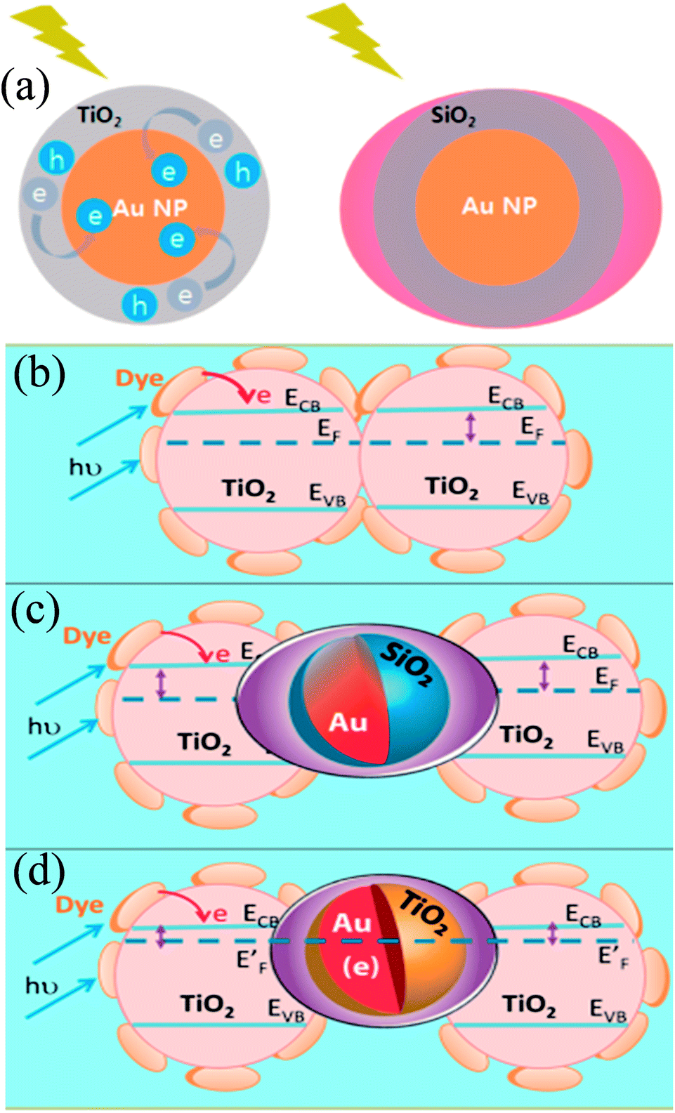
4.2 Effect of shell materials i.e. TiO2vs. SiO2
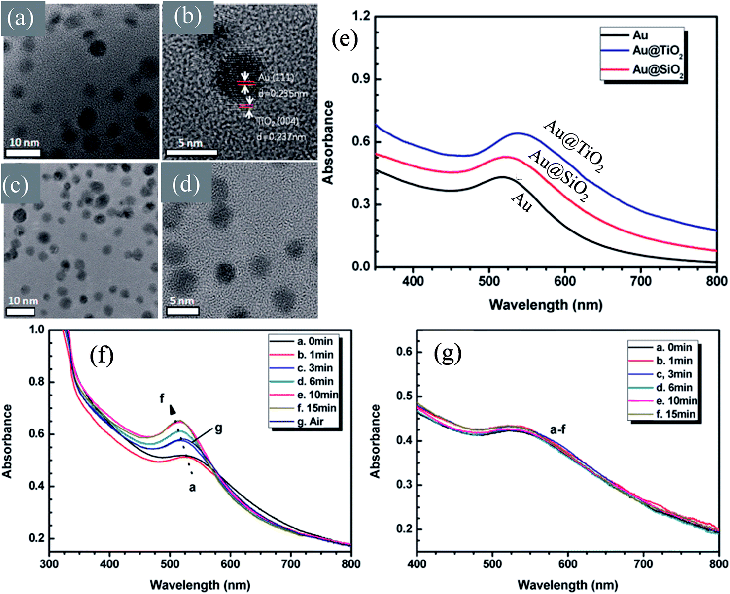
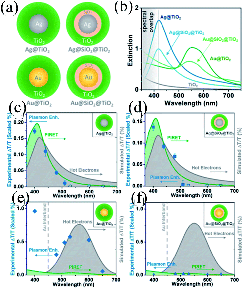
In recent years, plasmonic metal@metal oxide core–shells NPs have been widely used to improve the performance of DSSCs.191–197 Multiple reasons have been identified in these studies as being responsible for the enhancement of DSSC performance, derived from the coupling of semiconductor nanostructures with plasmonic NPs in core–shell geometry. For example, plasmonic core–shell NPs can increase solar absorption due to the LSPR and light-trapping effects of plasmonic NPs. Plasmonic core–shell NPs can also improve charge separation due to their localized electromagnetic field, and hence improve DSSC performance. Furthermore, the electron storage effects of plasmonic NPs can drive the Fermi level to more negative potentials, promoting electron transfer to adsorbed species, improving the device performance. However, electron storage in metal NPs also results in their photocharging. Meanwhile, the effect of photocharging of the metal core on DSSC performance had not been considered in these studies. Therefore, Kamat and co-workers investigated plasmonic and charging effects in DSSCs by capping Au NPs with SiO2 and TiO2, respectively.198 The thickness of either TiO2 or SiO2 shells was in the range of 0.7–1.0 nm and the Au core was 5–6 nm in diameter (Fig. 21a–d). The SPR band of Au@SiO2 and Au@TiO2 core–shell NPs was recorded at 527 and 542 nm, respectively, which were red-shifted as compared to the Au NPs (518 nm) as shown in Fig. 21e. After UV irradiation, the surface plasmon band of Au@TiO2 shifted from 530 nm to 516 nm (Fig. 21f), whereas no shift was recorded for Au@SiO2 (Fig. 21g). Thus, the blue-shift of the surface plasmon band of Au@TiO2 confirms the increase in electron density in the Au core due to the electron transfer process, as the plasmon frequency is directly proportional to the square root of the electron density (eqn (6)). It is worth mentioning that metal NPs undergo double-layer charging to stabilize stored electrons in an inert atmosphere. Thus, SiO2 being an insulator prevents electron charging of the metal core and exhibits only plasmonic effect. In contrast, TiO2 exhibits both plasmonic as well as charging effects because it is a semiconductor, and therefore capable of electron charging of the metal core.
 |
| | Fig. 21 TEM and HRTEM images of (a and b) Au@TiO2 and (c and d) Au@SiO2 NPs. (e) Absorption spectra of Au, Au@SiO2, and Au@TiO2 suspensions in toluene. Absorption spectra recorded following UV-irradiation of (f) Au@TiO2 and (g) Au@SiO2 colloidal suspensions in toluene/ethanol (1:1): (a) 0, (b) 1, (c) 3, (d) 6, (e) 10, and (f) 15 min of UV-irradiation. Reprinted with permission from ref. 198. Copyright 2012 American Chemical Society. | |
Finally, 0.7% wt% of Au@TiO2 and Au@SiO2 core–shell NPs were incorporated in two separate TiO2 based photoanodes having a similar amount of dye. The efficiency of conventional DSSCs (9.3%) was increased after the incorporation of plasmonic core–shell NPs. However, the efficiency of Au@SiO2 based DSSCs (10.2%) was slightly higher than that of Au@TiO2 based ones (9.8%). As displayed in Fig. 22c, Au@SiO2 core–shell NPs show only plasmonic effects, and hence their electrode (Jsc of 20.31 mA cm−2) exhibits an increase in photocurrent compared to the bare TiO2 based electrode (Jsc of 18.28 mA cm−2) without any significant change in its open circuit voltage (Voc of 0.728 V). However, electrodes based on Au@TiO2 core–shell show an increase of 42 mV in open-circuit voltage as compared to the bare TiO2 based electrodes (Voc of 0.729 V) without affecting photocurrent (Jsc of 18.28 mA cm−2) due to charging and plasmonic effects as depicted in Fig. 22d. The increase in the open circuit voltage of the electrode basically results from the charging effect of Au@TiO2, which has allowed the shift of the Fermi level to a more negative potential. These results clearly distinguish the charging and plasmonic effects and their consequences on DSSC performance. For example, charging effects in Au@TiO2 minimize plasmonic effects, and hence its efficiency was slightly lower than the Au@SiO2 core–shell NP based electrodes.
 |
| | Fig. 22 (a) Charging effect (Au@TiO2) versus plasmonic effect (Au@SiO2) of metal core oxide shell particles. Electron equilibration and its influence on the apparent Fermi level (EF): (b) dye TiO2 (c) dye TiO2/Au@SiO2, and (d) dye TiO2/Au@TiO2. Reprinted with permission from ref. 198. Copyright 2012 American Chemical Society. | |
Although, SiO2 is, in principle, a better shell material than TiO2 because the former results only in plasmonic effects (i.e., charge effects are avoided), it also reduces the effectiveness of plasmonic NPs as its large band gap does not allow the electron injection from molecular dyes into SiO2. Furthermore, dye molecules are physisorbed on SiO2 while being chemisorbed on TiO2. Therefore, Sheehan et al. proposed a new multilayered structure (Au@SiO2@TiO2) where SiO2 was coated with a thin layer of TiO2, so that electrons can be injected directly into the TiO2 shell.199 The Au@SiO2@TiO2 multi core–shell NPs (4.60%) have shown higher efficiency than Au@SiO2 core–shell NPs (4.04%). Furthermore, with the increase in thickness of TiO2 of Au@SiO2@TiO2 multi core–shell NPs, efficiency decreases due to a decrease in surface roughness and hence surface area for dye loading.
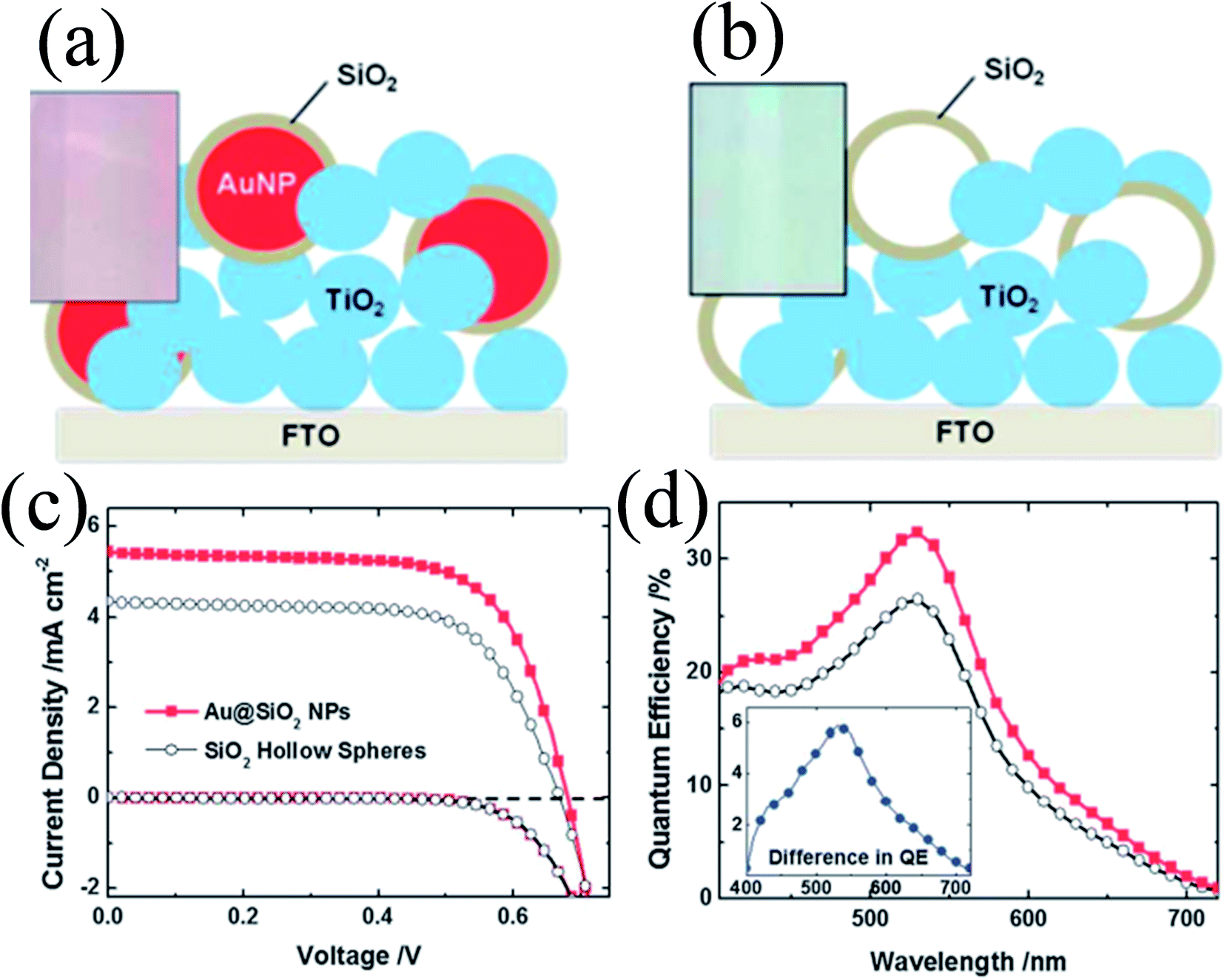
The above-mentioned studies clearly show that the metal core and oxide shell both affect the properties of plasmonic DSSCs; however in none of these studies the effect of the metal core and oxide shell is evaluated separately. Therefore, Wooh et al. synthesized Au@SiO2 core–shell NPs and SiO2 hollow spheres and incorporated them into TiO2 based photoanodes to investigate their effect on DSSC performance (Fig. 23a and b).200 SiO2 hollow spheres have the same morphology as the SiO2 shell of Au@SiO2 core–shell NPs as they were prepared by selective etching of Au cores. It is worth mentioning that the Au cores were dissolved in an iodide electrolyte in a few hours by penetrating the thin silica shell. Therefore, the SiO2 shell was treated with TiCl4 to block the penetration of the iodide electrolyte and ensure the stability of the Au NPs against dissolution. It has been found that the efficiency of the Au@SiO2 core–shell NP incorporated anode (2.66%) was higher than those with hollow SiO2 spheres (1.97%) confirming that the enhancement is mostly due to the LSPR effects of the Au NPs. However, in a similar study, we found that the use of hollow TiO2 has also increased the conversion efficiency.168 The hollow TiO2 NPs (150–200 nm in diameter) were produced by selective etching of the as-prepared Au@TiO2 core–shell NPs and applied as a scattering layer on top of a nanocrystalline TiO2 film. The efficiency was increased (from 5.2% to 7.4%) with hollow TiO2 spheres mainly because of light scattering and increase in the surface area.
 |
| | Fig. 23 Schemes of the TiO2 photoanodes incorporating (a) Au@SiO2 NPs and (b) SiO2 hollow spheres. Photographs of the corresponding photoanodes are shown in the insets. (c) Photocurrent–voltage characteristics and (d) IPCE spectrum of DSCs characterized with the inclusion of Au@SiO2 NPs (the red closed squares) and SiO2 hollow spheres (the black open circles). Reprinted with permission from ref. 200. Copyright 2013 Royal Society of Chemistry. | |
4.3 Effect of shell thickness
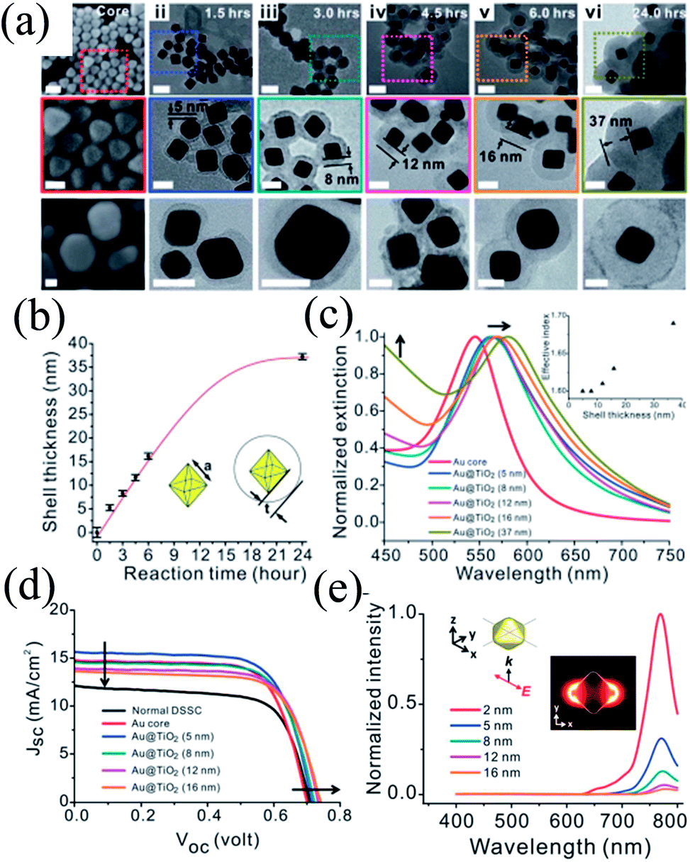
The distance between plasmonic NPs and dye molecules plays an important role in efficiency enhancement as the optical near-field decays rapidly from the metal–dielectric boundaries, and hence a thinner shell is preferred to get a stronger enhancement.201,202 Meanwhile, a thinner shell also results in quenching of dye molecules through non-radiative decay, i.e. electron or energy transfer to the metal surface.203,204 Therefore, the shell thickness of plasmonic core–shell NPs should be designed carefully to get full advantage of plasmonic enhancement in DSSCs. For example, Huang and co-workers precisely controlled the morphology of Au@TiO2 core–shell NPs to investigate its influence on the plasmonic enhancement (Fig. 24a).205 TEM images clearly show that cores have a well-defined octahedral shape (Fig. 24a–i), atomically flat crystal facets, and relatively narrow distribution of the side length (23.2 ± 1.1 nm) (Fig. 24b). They used octahedral Au NPs mainly because octahedral cores exhibit a higher near-field enhancement around the corners, whereas commonly used spherical Au NPs create random hot-spots due to their irregular shape and corrugated surface.206 The SPR peak of the Au core (545 nm) was red-shifted from 560 to 570 nm as the TiO2 shell thickness was increased from 5 to 16 nm, respectively (Fig. 24c).
 |
| | Fig. 24 (a) SEM images of the octahedral cores (i) and TEM images of the Au@TiO2 core–shell NPs with increasing reaction time and shell thickness (ii–vi). Middle panels show the zoomed-in images of the areas marked with dotted squares in the corresponding top panels. Bottom panels show the images of the corresponding NPs after being sintered at 500 °C for 1 hour. Scale bars for top, middle and bottom panels are 50, 25 and 20 nm, respectively. (b) Shell thickness as a function of reaction time. (c) Extinction spectra of octahedral gold cores (red) and Au@TiO2 NPs with shell thicknesses of 5, 8, 12, 16, and 37 nm (blue, cyan, magenta, orange and dark yellow, respectively). The inset shows the simulated effective index of the shell as a function of the thickness. (d) The J–V curves of plasmonic DSSCs with optimal doping levels that give the best efficiency. (e) Simulated near-field spectra recorded at positions that are 2 nm (red), 5 nm (blue), 8 nm (cyan), 12 nm (magenta) and 16 nm (orange) from the surface of the gold core. The inset shows the coordination and the polarization of the incident excitation as well as the near-field enhancement distribution recorded at 766 nm. Reprinted with permission from ref. 205. Copyright 2013 Royal Society of Chemistry. | |
Thus, addition of Au@TiO2 core–shell NPs with a 5 nm shell improved the efficiency from 6.00% (normal DSSCs) to 7.38% (plasmonic DSSCs), which decreased with a further increase in shell thickness (Fig. 24d). It has been found that Au@TiO2 core–shell NPs having a thinner TiO2 shell enhanced the short-circuit current due to an enhancement in the excitation rate of dye. Meanwhile, Au@TiO2 core–shell NPs with a thicker TiO2 shell increased the open-circuit voltage due to the charge equilibrium between the semiconductor and the metal cores. In an interesting note, they proposed that thinner TiO2 behaves like an insulating layer as SiO2. Therefore, plasmonic near-field enhancement decreased with an increase in shell thickness and hence, the plasmonic excitation of dye also diminished. Furthermore, the SPR band red-shifted with an increase in shell thickness; however this has little impact on plasmonic enhancement, as efficiency decreased with the increase in shell thickness. They suggested that the enhancement in efficiency was also related to the plasmonic heating effect, which has promoted the electrochemical reaction in the cell and increased the mobility of the electrolyte, thus enhancing the short-circuit current.207
Thus, the distance between the metal and dye, i.e., shell thickness should be short for near-field plasmonic enhancement. However, too short a distance also results in loss of photocurrent via non-radiative damping, called surface energy transfer (SET). Thus, plasmonic enhancement and non-radiative quenching both co-exist simultaneously in plasmonic DSSCs. Therefore, Huang and co-workers synthesized Ag@SiO2@TiO2 multi core–shell NPs with variable SiO2 shell thickness to get an optimal dielectric shell thickness for the best device performance.208 The TiO2 shell (1 nm) was used to facilitate the chemisorption of dye molecules, as physisorption takes place on the SiO2 shell, for efficient electron injection to TiO2 NPs. Furthermore, an insulating SiO2 shell was used to prevent the recombination and back reaction of photogenerated carriers with the Ag core. The effect of the distance between the Ag core and dye molecules on plasmonic enhancement and non-radiative quenching has been systematically investigated using five types of cells, namely, pure TiO2, Ag@TiO2, and Ag@SiO2@TiO2 with 5, 10 and 20 nm SiO2 shells. It has been found that plasmonic enhancement was dominant for the SiO2 shell with a thickness smaller than 10 nm and hence, an enhancement in efficiency was also found. However, SET became dominant when the shell thickness was decreased below 5 nm, and therefore photovoltaic performance was highly suppressed.
4.4 Effect of core materials
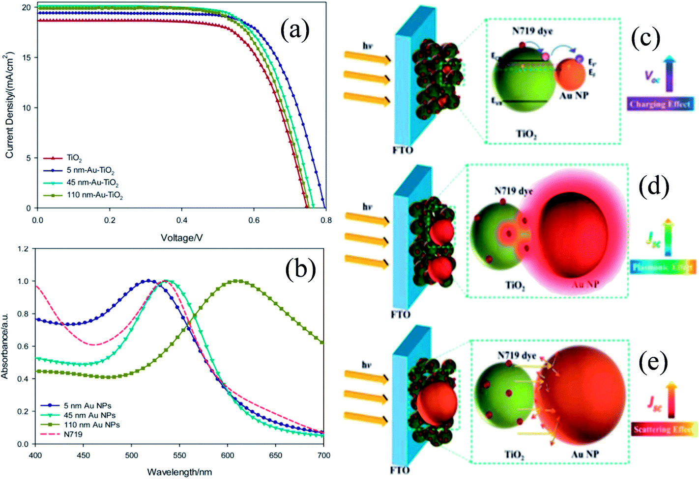
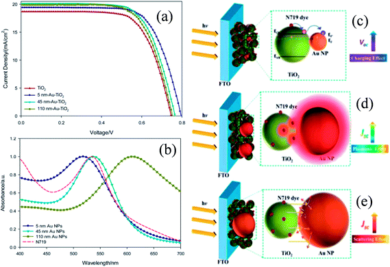
The shape, size, and composition of plasmonic NPs affect their SPR characteristics and hence, their effect on the characteristics of DSSCs also needs to be investigated. For example, an effective plasmonic enhancement was found for 36 nm Ag and 5 nm Au cores when the shell thickness was 5 and 1 nm, respectively, which indicates the importance of the size of core materials in DSSC applications.192,198 Thus, Wang et al. synthesized Au@TiO2 core–shell NPs with three different Au NPs sizes (5, 45 and 110 nm) in order to investigate photocharging, plasmonic, and scattering effects on DSSC performance.209 The short-circuit current density and hence the efficiency of conventional TiO2 DSSCs (9.59%) was increased with the addition of plasmonic core–shell NPs (10.80%, 10.52%, and 10.20% for Au@TiO2 core–shell NPs with 5, 45, and 110 nm Au NPs, respectively) (Fig. 25a). The enhancement in efficiency was basically related to the light harvesting efficiency of plasmonic NPs (Fig. 25b). Thus, plasmonic DSSCs with the 45 nm Au core showed the highest efficiency because their absorption spectra showed a maximum overlap with the absorption spectra of dye molecules. Although, the spectral match between the dye and 5 nm Au core was weak, the improvement observed in DSSC performance was related to the increase in open-circuit voltage. The increase in open-circuit voltage results in charge separation i.e. longer electron lifetime, which has improved efficiency. The improvement in the performance of plasmonic DSSCs with the 110 nm Au core was primarily related to the light scattering effect. Thus, the size of plasmonic NPs greatly affects the performance of DSSCs as a result of plasmonic, photocharging and scattering effects.
 |
| | Fig. 25 (a) J–V curves of Au@TiO2-DSSCs and TiO2-DSSCs under AM-1.5G one sun irradiation. (b) UV-Vis absorbance spectra of different-sized Au NPs in water (solid line) and N719 dye in ethanol (dashed line). Schematic illustration of the (c) photocharging effect of 5 nm Au NPs, (d) plasmonic effect of 45 nm Au NPs, and (e) scattering effect of 110 nm Au NPs. Reprinted with permission from ref. 209. Copyright 2013 Royal Society of Chemistry. | |
Most commonly used spherical NPs of either silver or gold in DSSCs absorb light in the visible region (basically 400–550 nm), where the N719 dye already absorbs strongly and thus, diminishes the need for plasmonic enhancement. So, to improve the light harvesting capability of the dye, one would need plasmonic NPs that can absorb light more strongly in the 550–700 nm range, where the dye absorbs weakly. Therefore, Kelly and co-workers incorporated anisotropic Au@SiO2 core–shell NPs in DSSCs and efficiency (8.4%) was improved by 32% as compared to TiO2 based DSSCs mainly because triangular Ag nanoprisms increased the light harvesting efficiency in the red and near-infrared regions.138 They found that annealing (at 450 °C) of triangular Ag@SiO2 nanoprisms produced a blue-shift of the SPR band, which resulted in a better overlap with the absorption spectrum of black dye, which enabled obtaining a 15% increase in efficiency (from 3.9 to 4.4).139 Zarick et al. synthesized Au@SiO2 core–shell NPs with Au nanocubes of controlled shape and incorporated them in photoanodes to enhance the performance of DSSCs.210 The efficiency of plasmonic DSSCs (7.8%) was increased by 34% as compared to conventional DSSCs (5.8%). This improvement was attributed to a quasistatic lightning-rod effect in Au nanocubes. The lightning-rod effect resulted in intense electromagnetic fields at the edges and corners of Au nanocubes, which has increased the plasmonic coupling, carrier generation and hence efficiency. This phenomenon was further confirmed by Bai et al., who synthesized Au@TiO2 core–shell with spherical and concave cubic shape core NPs and investigated their effect on plasmonic enhancement of DSSCs (Fig. 26a and b).211 The SPR band of concave cubic Au@TiO2 core–shell NPs was red-shifted (695 nm) as compared to spherical ones (601 nm), which was further shifted up to 865 nm with increasing TiO2 shell thickness as shown in Fig. 26c. Furthermore, cubic Au@TiO2 core–shell NPs (9.09%) have shown higher efficiency than spherical ones (8.46%) and efficiency decreased with an increase in shell thickness as displayed in Fig. 26d. The improvement in performance was attributed to the presence of hot-spots (sharp corners and edges of metal NPs) in cubic Au@TiO2 core–shell NPs which resulted in higher light harvesting and more efficient charge separation as compared to the spherical metal NPs with a smooth surface. Chang et al. incorporated Ag2S-encapsulated Au nanorods (Au@Ag2S) in TiO2 based DSSCs and found that the efficiency was increased from 5.8% to 7.1%.212 The improvement in efficiency was attributed to the broad absorption spectrum of Au@Ag2S (ranging from 400 to 900 nm) and hence, sunlight can effectively couple with plasmon absorption in this range. Researchers have also tried core@shell structures with multiple shells to achieve broadband light harvesting in DSSCs especially in the NIR region where the light absorption by the N719 dye is weak.213
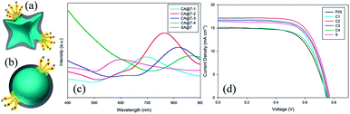 |
| | Fig. 26 Schematic illustration of a superior LSPR effect induced by (a) hot-spot-containing concave cubic Au@TiO2 core–shell NPs in comparison with (b) normal spherical Au@TiO2 core–shell NPs, (c) their absorption spectra in ethanol and (d) I–V characteristics of DSSCs based on a variety of working electrodes. Reprinted with permission from ref. 211. Copyright 2015 Elsevier. | |
Recently, Li et al. have incorporated asymmetric Au–SiO2 clusters with a number of Au NP off-centers in DSSCs instead of conventional Au@SiO2 core–shell NPs (Fig. 27a–c).146 It is interesting to note that the SPR band of Au–SiO2 clusters red-shifted (530–560 nm) with an enhancement in intensity as the number of Au NPs increased, which is attributed to the near-field coupling between Au NPs (Fig. 27d). Thus, the efficiency of plasmonic DSSCs was improved from 1.79 to 2.24% as displayed in Fig. 27e. The improvement in efficiency was attributed to the strong optical interaction between Au NPs and adsorbed dye molecules at the thinner SiO2 side of the asymmetric Au–SiO2 cluster. Similarly, Au–TiO2 photoanodes with a mosaic structure of 2 nm Au NPs directly inlaid in a TiO2 working electrode has improved the efficiency of plasmonic DSSCs (10.1%) as compared to conventional ones (5.5%).214
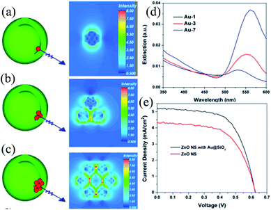 |
| | Fig. 27 Plasmonic near-field maps (cross-sectional view at x = 0, incident light from the x direction and polarization along the y axis) simulated using DDA for the Au–SiO2 asymmetric clusters with different amounts of Au NPs: (a) one Au NP; (b) three Au NPs; and (c) seven Au NPs, (d) optical extinction spectra, and (e) J–V curve of ZnO nanosheets with and without Au–SiO2 asymmetric clusters. Reprinted with permission from ref. 146. Copyright 2013 American Chemical Society. | |
Thus, spheroidal nanostructures improve the efficiency of DSSCs simply by LSPR and light scattering effects which increase the light absorption of the dye and lower the rate of recombination. However, these effects can be experienced only in a limited area as spheroidal NPs do not provide a path for light or electrons to be transported efficiently in the photoanode. Therefore, Ag@TiO2 core–shell nanowires, having Ag nanowires as the core, were incorporated in photoanodes to exploit the potentials of the plasmonic metal nanostructures (Fig. 28).177 The efficiency of plasmonic DSSCs (8.84%) was remarkably improved as compared to conventional DSSCs (6.16%), which is attributed to their unique “optics-electrics expressways” characteristics. The plasmonic waveguide effect of Ag nanowires has effectively increased the light path in the photoanode and hence, improved the light harvesting efficiency of the dye far away from the incident light.215,216
 |
| | Fig. 28 (a) Schematic diagram of the photoelectron transporting process in photoanodes of pure TiO2 DSSCs and nanocomposite modified DSSCs (inset shows SEM images of the AgNW@TiO2 nanocomposites). (b) J–V characteristic of DSSCs with various TiO2 photoanodes. Reprinted with permission from ref. 177. Copyright 2014 Elsevier. | |
The electron transport in the photoanode was also promoted via coating a carbon layer on Au@TiO2 core–shell NPs. For example, Zheng et al. synthesized carbon coated Au@TiO2 core–shell NPs via carbonization of polystyrene capped Au@TiO2 core–shell NPs in an inert environment.217 The efficiency of carbonized Au@TiO2 incorporated DSSCs was increased from 5.67 to 6.44% as compared to conventional TiO2 based DSSCs. The efficiency enhancement was related to plasmonic enhancement as well as electron transport promoted by the carbon layer. A similar enhancement was also observed when graphene was used in Au@SiO2 based DSSCs.218
It is reported in the literature that the optical absorption of DSSCs can be increased by increasing the number of plasmonic NPs incorporated in photoanodes.219 However, Ag or Au NPs show quenching of carriers at high concentration, and therefore researchers are trying to find new plasmonic NPs.220,221 For example, Huang and co-workers used plasmonic aluminium (Al) NPs to enhance DSSC performance.220 The Al NPs showed better chemical stability in an iodide electrolyte as compared to noble metals. The efficiency of plasmonic DSSCs was improved from 6.15 to 6.95%, where a low work function of Al (∼4.06 eV) as compared to TiO2 (∼4.6 eV) has reduced the loss induced by charge transfer. Similarly, alloys of Ag and Au NPs have been used to enhance the performance of DSSCs, where the plasmonic effect of the Au–Ag alloy significantly enhanced the broadband light absorption of dye molecules.222,223
4.5 Solid-state DSSCs
In conventional DSSCs, mostly iodide/triiodide ion based liquid electrolytes are used which are volatile and corrosive in nature. Therefore, researchers are developing solid-state hole-transport materials (Spiro-OMeTAD) to solve the potential leakage problems of liquid electrolytes. The efficiency of DSSCs can also be improved by tuning open-circuit voltage via adjusting the highest-occupied molecular orbital (HOMO) of the hole-transport materials.224,225 However, there are only a few reports on the use of plasmonic NPs in solid-state DSSCs.226,227 For example, Ding et al. incorporated plasmonic back reflectors consisting of 2D arrays of Ag nanodomes into solid-state DSSCs by nanoimprint lithography.226 They achieved 3.9 and 5.9% efficiencies for solid-state DSSCs made with Z907 and C220 dyes, respectively. They proposed that the enhancement in efficiency was basically related to the SPR and scattering-induced effects of 2D arrays of Ag nanodomes.
4.6 Plasmon enhancement mechanism
The use of plasmonic NPs improves the performance of DSSCs. The effect of various plasmonic noble metal@metal oxide core–shell NPs on the efficiency of DSSCs is summarized in Table 1.
Table 1 A summary of materials design for plasmonics enhancement of DSSCs and the corresponding mechanisms
| Plasmonic core–shell NPs |
Reference efficiency (%) |
Plasmonic efficiency (%) |
Responsible factors |
Ref. |
|
(A) Effect of plasmonic core–shell
|
| Ag@TiO2 core–shell |
0.2 (TiO2) |
1.4 |
Plasmonic effect |
192
|
| Au@SiO2 core–shell |
1.05 (TiO2) |
1.95 |
Plasmonic effect |
196
|
| Ag@TiO2 core–shell |
3.1 (TiO2) |
4.4 |
Plasmonic and conducting effect of TiO2 |
197
|
| Au@SiO2 core–shell |
9.3 (TiO2) |
10.2 |
Plasmonic effect |
198
|
| Au@TiO2 core–shell |
9.3 (TiO2) |
9.8 |
Plasmonic and charging effect |
198
|
| Au@SiO2/TiO2 core–shell |
3.07 (TiO2) |
4.6 |
Plasmonic and conducting effect of TiO2 |
199
|
|
|
(B) Effect of shell thickness
|
| Au@TiO2 core–shell |
6.0 (TiO2) |
7.38 (5 nm) |
Plasmonic and heating effect |
205
|
| 7.22 (8nm) |
| 6.95 (12 nm) |
| 7.04 (16 nm) |
| Ag@SiO2/TiO2 core–shell |
3.73 (TiO2) |
4.00 (5 nm SiO2) |
Plasmonic and SET effect |
208
|
| 4.02 (10 nm SiO2) |
| 3.68 (20 nm SiO2) |
|
|
(C) Effect of core materials
|
| Au@TiO2 core–shell |
9.59 (TiO2) |
10.8 (5 nm Au) |
Photocharging effect |
209
|
| 10.52 (45 nm Au) |
Plasmonic effect |
| 10.2 (110 nm Au) |
Scattering effect |
| Au@SiO2 core–shell |
5.8 (TiO2) |
7.8 |
Lightning-rod effect in Au nanocubes |
210
|
| Au@TiO2 core–shell |
7.37 (TiO2) |
8.46 (Spherical) |
Plasmonic effect |
211
|
| 9.09 (Cubic) |
Presence of hot-spots |
| Au@Ag2S core–shell (Au nanorods) |
5.8 (TiO2) |
7.1 |
Broad absorption spectrum (400-900 nm) |
212
|
| Au@SiO2 core–shell (Clusters of Au NPs) |
1.79 (ZnO) |
2.24 |
Plasmonic effect |
146
|
| Au@TiO2 mosaic |
5.5 (TiO2) |
10.1 |
Plasmonic and reduced charge |
214
|
| Ag@TiO2 core–shell (Ag nanowires) |
6.16 (TiO2) |
8.84 |
Plasmonic waveguide effect of Ag nanowires |
177
|
Several mechanisms have been reported in the literature on the effect of plasmonic NPs in DSSCs, such as near-field enhancement, light scattering, hot-electron injection, non-radiative damping, etc. However, it is unclear whether these enhancement mechanisms co-exist or compete with each other and how they can be controlled in order to fabricate high performance DSSCs. Therefore, the working principle of plasmonic NPs and their positive and negative impact on DSSCs is summarized in this section. Plasmonic enhancement in DSSCs depends on three basic mechanisms, such as photonic enhancement, direct electron transfer (DET) also known as hot-electron injection, and plasmon-induced resonance energy transfer (PIRET).228 In photonic enhancement, SPR improves the light absorption capability of semiconductors via their interaction in far-field radiation.229,230 The hot-electron injection or PIRET involves improvement in above-band-edge and below-band-edge photoconversion via interaction of plasmons with the semiconductor in near-field radiation.231–234 It is noteworthy that charge separation in semiconductors occurs at the wavelength where plasmonic NPs absorbs the incident light and not at the wavelength where semiconductors absorb light. First of all, Cushing et al. studied the impact of hot-electron injection and PIRET in DSSCs in detail.235 It is well known that physical contact and spectral overlap are the two key factors governing the hot-electron injection and PIRET processes. For example, hot-electron injection involves the transfer of electrons from the metal to the semiconductor through a Schottky barrier, and hence a direct contact between plasmonic NPs and the semiconductor is required for this process.236 However, PIRET involves spectral overlap between plasmonic NPs and semiconductors and hence, does not require a physical contact between them, except that the semiconductor should be present within the plasmon's near-field. To fulfill hot-electron injection and PIRET requirements, a set of metal@TiO2 core–shell NPs have been designed with various spectral overlaps and contacts between plasmonic NPs and metal oxide semiconductors as displayed in Fig. 29a and b.235 For example, both hot-electron injection and PIRET are possible in Ag@TiO2 due to the spectral overlap between the Ag NP plasmon and TiO2 absorption tail. In contrast, only hot-electron injection is possible in Au@TiO2 core–shell due to the lack of spectral overlap between the Au core and TiO2 shell. If an insulating SiO2 shell is placed in between the metal core and TiO2 shell, then hot-electron injection becomes impossible and only PIRET is possible. Therefore, only PIRET is possible in Ag@SiO2@TiO2 core–shell NPs, whereas neither hot-electron injection nor PIRET is possible in Au@SiO2@TiO2 core–shell NPs. The results of theoretical prediction of PIRET and hot-electron injection and measured enhancement in DSSCs are given in Fig. 29c–f. In Ag@TiO2, although both hot-electron injection and PIRET are present, PIRET played the dominant role in the overall enhancement of charge carrier photogeneration, as shown in Fig. 29c. The enhancement in charge carrier photogeneration for Ag@SiO2@TiO2 was dominated by PIRET as hot-electron injection was blocked by insulating SiO2 (Fig. 29d). In Au@TiO2 only hot-electron injection is possible, and hence a transient absorption signal was observed to follow the plasmon's absorption band shape, which is consistent with the theoretical prediction as displayed in Fig. 29e. Neither PIRET nor hot-electron injection is possible in Au@SiO2@TiO2, and hence no plasmonic enhancement was observed below the band edge of TiO2 (Fig. 29f).
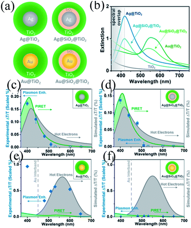 |
| | Fig. 29 (a) Schematic of metal core@TiO2 shell NPs. (b) Extinction spectra of various metal core@TiO2 shell NPs as well as TiO2 alone. The theoretical enhancement predicted for PIRET and hot electrons is shown as filled curves. (c) In Ag@TiO2 a contact and spectral overlap exist between the metal and semiconductor, and PIRET and hot electron injection are both measured. (d) Addition of a SiO2 barrier to Ag@TiO2 eliminates hot electron injection. (e) Switching the metal core to Au eliminates spectral overlap and PIRET. (f) Inserting a SiO2 barrier in Au@TiO2 eliminates both hot electron injection and PIRET despite strong light absorption by plasmonic Au. Reprinted with permission from ref. 235. Copyright 2015 American Chemical Society. | |
Furthermore, the coupling of sensitizers with plasmonic NPs can also enhance the efficiency of photoinduced electron transfer from sensitizers to semiconductors.237 The injection dynamics depend on the coupling of electronic excitations in sensitizers with plasmons of NPs. Thus, an optimum or threshold value of coupling is needed at which the injection efficiency can be maximized and these values depend on various competing processes, including electron transfer and the Purcell effect. Thus, the optimum or threshold value is influenced by electron transfer and plasmon relaxation/dephasing time scales. Thus, the ability to optimize the electron transfer and to modify its dynamics may have important implications for DSSCs as well as other solar cells because photoinduced electron transfer at interfaces is the fundamental physical process.
5. Miscellaneous applications of plasmonic noble metal@metal oxide core shell NPs
The application of the SPR of metal NPs is not only limited to DSSCs and has many applications, such as LEDs, sensors, catalysis, etc.238–265 For example, plasmonic NPs have also improved the performance of silicon or organic or perovskite solar cells through light trapping via light scattering and near-field enhancement.238–249 In sensing applications, plasmonic NPs act as transducers and convert the changes in the local refractive index into spectral shifts of the LSPR band.250–253 The specificity or selectivity of these sensors can be improved by attaching molecular recognition elements to the nanostructures. In photocatalysis, plasmonic NPs efficiently absorb solar light through LSPR, which is transferred to the semiconductor via PIRET and DET simultaneously, and thus improve the rate of electron–hole pair generation and decrease the rate of recombination.254–258 There are several other exciting research areas where plasmonic NPs are used to enhance the characteristics, such as light emitting diodes (LEDs).259–261 therapeutics,262,263 imaging,264,265etc.
6. Conclusion and outlook
In this review article, I have summarized the recent progress in the preparation of plasmonic core–shell NPs for DSSC applications, where Ag and Au NPs are used as the plasmonic core and TiO2 or SiO2 is used as the shell. Mostly, these core–shell NPs are prepared in two steps, where the core is prepared first and used as a template for shell formation. Various well-defined core–shell, yolk–shell and Janus nanostructures have been synthesized by wet-chemical methods. The formation of the metal oxide shell has not only protected the plasmonic NPs chemically and thermally, but also generated new optical properties. The SPR of plasmonic NPs was tuned from the UV to IR region by controlling the shape, size and shell thickness of core–shell NPs. The formation of the TiO2 or SiO2 shell on plasmonic NPs has solved the issue of corrosion of metal NPs in redox iodide electrolytes. The use of these plasmonic core–shell NPs has significantly improved the DSSC performance by improving the solar light harvesting of the photoanode. The inclusion of plasmonic core–shell NPs in the photoanode has also reduced the film thickness. It has been found that plasmonic NPs improved the performance via photonic enhancement, hot-electron injection, PIRET and light scattering processes. The key points for the fabrication of efficient plasmonic DSSCs are related to precise control over their desired size, shape, morphology, composition and concentration.
Although the results of plasmonic solar cells are promising, the efficiency of most of these solar cells needs to be further improved. The efficiency of DSSCs can be further improved either by extending the light harvesting region into the NIR or lowering the redox potential of the electrolyte to increase the open-circuit voltage. The biggest challenge in DSSCs is that dye molecules are not able to harvest a wide range of the solar spectrum; therefore multiple dyes can be used to boost the solar absorption. However, the use of multiple layers of dye increases the rate of recombination due to the slow transport of excited electrons into semiconductors, and hence it needs to be tackled for efficient DSSC fabrication. Another drawback of DSSCs is related to the low potential of the standard iodide redox couple, which introduces a large energy loss during the transfer of electrons from iodide ions to dye. Thus, a high potential redox couple is needed in order to fabricate efficient DSSCs with high efficiency. Furthermore, TiO2, which is widely used as a photoanode in DSSCs, can absorb only the UV region of the solar spectrum, and this limits the efficiency of DSSCs. Therefore, low band gap materials, such as Fe2O3 and WO3, can be used to harvest a broad solar spectrum in order to improve the efficiency. However, low band gap materials can decrease the PCE of DSSCs mainly because most of the incident light will be absorbed by the metal oxides rather than the dye molecules, as the photovoltaics of DSSC primarily depends on dye molecules. Several other issues, such as carrier lifetime and/or carrier diffusion characteristics, are associated with these materials, which need to be sorted out before their implementation. Furthermore, replacement of costly Pt from the counter electrode with some low cost materials is required in order to reduce the overall cost. For example, sulfides and selenides have been investigated as counter electrodes to replace Pt in DSSCs. Despite many limitations, more than 10% efficiency has been achieved in the last two decades, and therefore, researchers are still hopeful for further enhancement by the logical design of the device.
Conflicts of interest
There are no conflicts to declare.
Acknowledgements
P. Rai is supported by the Department of Science and Technology (DST), New Delhi, India vide DST-INSPIRE Faculty Scheme (DST/INSPIRE/04/2014/001318; IFA14/MS-20).
References
- F. C. Krebs, M. Hösel, M. Corazza, B. Roth, M. V. Madsen, S. A. Gevorgyan, R. R. Søndergaard, D. Karg and M. Jørgensen, Energy Technol., 2013, 1, 378–381 CrossRef.
- B. C. O'Regan and M. Graetzel, Nature, 1991, 353, 737–740 CrossRef.
- F. Bella, C. Gerbaldi, C. Barolob and M. Graetzel, Chem. Soc. Rev., 2015, 44, 3431–3473 RSC.
- G. Richhariya, A. Kumar, P. Tekasakul and B. Gupta, Renewable Sustainable Energy Rev., 2017, 69, 705–718 CrossRef CAS.
- A. Yella, H.-W. Lee, H. N. Tsao, C. Yi, A. K. Chandiran, M. Nazeeruddin, E. W.-G. Diau, C.-Y. Yeh, S. M. Zakeeruddin and M. Graetzel, Science, 2012, 334, 629–634 CrossRef PubMed.
- P. Wang, S. M. Zakeeruddin, J. E. Moser, M. K. Nazeeruddin, T. Sekiguchi and M. Gratzel, Nat. Mater., 2003, 2, 402–407 CrossRef CAS PubMed.
- M. K. Nazeeruddin, T. Bessho, L. Cevey, S. Ito, C. Klein, F. De Angelis, S. Fantacci, P. Comte, P. Liska, H. Imai and M. Graetzel, Renewable Sustainable Energy Rev., 2007, 185, 331–337 CAS.
- M. Graetzel, Acc. Chem. Res., 2009, 42, 1788–1798 CrossRef PubMed.
- I. Mora-Sero and J. Bisquert, J. Phys. Chem. Lett., 2010, 1, 3046–3052 CrossRef CAS.
- J. B. Sambur, T. Novet and B. A. Parkinson, Science, 2010, 330, 63–66 CrossRef CAS PubMed.
- M. Law, L. E. Greene, J. C. Johnson, R. Saykally and P. Yang, Nat. Mater., 2005, 4, 455–459 CrossRef CAS PubMed.
- K. Zhu, N. R. Neale, A. Miedaner and A. Frank, Nano Lett., 2007, 7, 69–74 CrossRef CAS PubMed.
- J. Villanueva-Cab, S. R. Jang, A. F. Halverson, K. Zhu and A. J. Frank, Nano Lett., 2014, 14, 2305–2309 CrossRef CAS PubMed.
- S.-Y. Shen, R.-X. Dong, P.-T. Shih, V. Ramamurthy, J.-J. Lin and K.-C. Ho, ACS Appl. Mater. Interfaces, 2014, 6, 18489–18496 CrossRef CAS PubMed.
- S. Mathew, A. Yella, P. Gao, R. Humphry-Baker, B. F. E. Curchod, N. Ashari-Astani, I. Tavernelli, U. Rothlisberger, M. K. Nazeeruddin and M. Gratzel, Nat. Chem., 2014, 6, 242–247 CrossRef CAS PubMed.
- X. Liu, J. Iocozzia, Y. Wang, X. Cui, Y. Chen, S. Zhao, Z. Li and Z. Lin, Energy Environ. Sci., 2017, 10, 402–434 RSC.
- H. A. Atwater and A. Polman, Nat. Mater., 2010, 9, 205–213 CrossRef CAS PubMed.
- C. Clavero, Nat. Photonics, 2014, 8, 95–103 CrossRef CAS.
- C. Wen, K. Ishikawa, M. Kishima and K. Yamada, Sol. Energy Mater. Sol. Cells, 2000, 61, 339–351 CrossRef CAS.
- W. Hou, P. Pavaskar, Z. Liu, J. Theiss, M. Aykol and S. B. Cronin, Energy Environ. Sci., 2011, 4, 4650–4655 RSC.
- R. A. Naphade, M. Tathavadekar, J. P. Jog, S. Agarkar and S. Ogale, J. Mater. Chem. A, 2014, 2, 975–984 RSC.
- Q. Xu, F. Liu, Y. Liu, K. Cui, X. Feng, W. Zhang and Y. Huang, Sci. Rep., 2013, 3, 2112 CrossRef PubMed.
- H. Jung, B. Koo, J.-Y. Kim, T. Kim, H. J. Son, B. S. Kim, J. Y. Kim, D.-K. Lee, H. Kim, J. Cho and M. J. Ko, ACS Appl. Mater. Interfaces, 2014, 6, 19191–19200 CrossRef CAS PubMed.
- W. R. Erwin, H. F. Zarick, E. M. Talbert and R. Bardhan, Energy Environ. Sci., 2016, 9, 1577–1601 RSC.
- Y. H. Jang, Y. J. Jang, S. Kim, L. N. Quan, K. Chung and D. H. Kim, Chem. Rev., 2016, 116, 14982–15034 CrossRef CAS PubMed.
- N. Zhang, S. Liu and Yi-J. Xu, Nanoscale, 2012, 4, 2227–2238 RSC.
- G. Li and Z. Tang, Nanoscale, 2014, 6, 3995–4011 RSC.
- P. Rai, S. M. Majhi, Y.-T. Yu and J.-H. Lee, RSC Adv., 2015, 5, 76229–76248 RSC.
- R. Jiang, B. Li, C. Fang and J. Wang, Adv. Mater., 2014, 26, 5274–5309 CrossRef CAS PubMed.
- P. Rai, J.-W. Yoon, H.-M. Jeong, S.-J. Hwang, C.-H. Kwak and J.-H. Lee, Nanoscale, 2014, 6, 8292–8299 RSC.
- W. Ye, R. Long, H. Huang and Y. Xiong, J. Mater. Chem. C, 2017, 5, 1008–1021 RSC.
- K. A. Willets and R. P. Van Duyne, Annu. Rev. Phys. Chem., 2007, 58, 267–297 CrossRef CAS PubMed.
- K. M. Mayer and J. H. Hafner, Chem. Rev., 2011, 111, 3828–3857 CrossRef CAS PubMed.
- S. K. Ghosh and T. Pal, Chem. Rev., 2007, 107, 4797–4862 CrossRef CAS PubMed.
- S. Pillai and M. A. Green, Sol. Energy Mater. Sol. Cells, 2010, 94, 1481–1486 CrossRef CAS.
- J. A. Scholl, A. L. Koh and J. A. Dionne, Nature, 2012, 483, 421–427 CrossRef CAS PubMed.
- C. M. Y. Yeung and S. C. Tsang, J. Phys. Chem. C, 2009, 113, 6074–6087 CrossRef CAS.
- V. E. Ferry, J. N. Munday and H. A. Atwater, Adv. Mater., 2010, 22, 4794–4808 CrossRef CAS PubMed.
- S. Linic, U. Aslam, C. Boerigter and M. Morabito, Nat. Mater., 2015, 14, 567–576 CrossRef CAS PubMed.
- K. R. Catchpole and A. Polman, Opt. Express, 2008, 16, 21793–21800 CrossRef CAS PubMed.
- G. H. Chan, J. Zhao, G. C. Schatz and R. P. Van Duyne, J. Phys. Chem. C, 2008, 112, 13958–13963 CrossRef CAS.
- O. A. Yeshchenko, I. M. Dmitruk, A. A. Alexeenko, A. V. Kotko, J. Verdal and A. O. Pinchuk, Plasmonics, 2012, 7, 685–694 CrossRef CAS.
- A. Pinchuk and U. Kreibig, New J. Phys., 2003, 5, 151.1–151.15 CrossRef.
- S. Peng, J. M. McMahon, G. C. Schatz, S. K. Gray and Y. Sun, PNAS, 2010, 107, 14530–14534 CrossRef CAS PubMed.
- G. Weick, G. L. Ingold, R. A. Jalabert and D. Weinmann, Phys. Rev. B, 2006, 74, 165421 CrossRef.
- N. K. Pathak and R. P. Sharma, Plasmonics, 2016, 11, 713–719 CrossRef CAS.
- P. Rai, S. M. Majhi, Y.-T. Yu and J.-H. Lee, RSC Adv., 2015, 5, 17653–17659 RSC.
- X. M. Lu, M. Rycenga, S. E. Skrabalak, B. Wiley and Y. N. Xia, Annu. Rev. Phys. Chem., 2009, 60, 167–192 CrossRef CAS PubMed.
- S. M. Majhi, P. Rai, S. Raj, B.-S. Chon, K.-K. Park and Y. Yeon-Tae, ACS Appl. Mater. Interfaces, 2014, 6, 7491–7497 CrossRef CAS PubMed.
- Y. Xia, Y. Xiong, B. Lim and S. E. Skrabalak, Angew. Chem., Int. Ed., 2009, 48, 60–103 CrossRef CAS PubMed.
- Y.-F. C. Chau, C. M. Lim, C. Lee, H. J. Huang, C.-T. Lin, N. T. R. N. Kumara, V. N. Yoong and H.-P. Chiang, J. Appl. Phys., 2016, 120, 093110 CrossRef.
- A. Pescaglini and D. Iacopino, J. Mater. Chem. C, 2015, 3, 11785–11800 RSC.
- N. K. Pathak, G. K. Pandey, A. Ji and R. P. Sharma, Plasmonics, 2015, 10, 1597–1606 CrossRef CAS.
- J. J. Mock, M. Barbic, D. R. Smith, D. A. Schultz and S. Schultz, J. Chem. Phys., 2002, 116, 6755–6759 CrossRef CAS.
- S. Eustis and M. A. El-Sayed, Chem. Soc. Rev., 2006, 35, 209–217 RSC.
- D. C. Tzarouchis, P. Ylä-Oijala, T. Ala-Nissila and A. Sihvola, Appl. Phys. A, 2016, 122, 298 CrossRef.
- C. Noguez, J. Phys. Chem. C, 2007, 111, 3806–3819 CrossRef CAS.
- E. Ringe, M. R. Langille, K. Sohn, J. Zhang, J. Huang, C. A. Mirkin, R. P. Van Duyne and L. D. Marks, J. Phys. Chem. Lett., 2012, 3, 1479–1483 CrossRef CAS PubMed.
- L. M. Liz-Marzan, Langmuir, 2006, 22, 32–41 CrossRef CAS PubMed.
- N. C. Dyck, R. C. Denomme and P. M. Nieva, J. Phys. Chem. C, 2011, 115, 15225–15233 CrossRef CAS.
- W.-S. Chang, J. Won Ha, L. S. Slaughter and S. Link, PNAS, 2010, 107, 2781–2786 CrossRef CAS PubMed.
- M. A. Mahmoud, M. Chamanzar, A. Adibi and M. A. El-Sayed, J. Am. Chem. Soc., 2012, 134, 6434–6442 CrossRef CAS PubMed.
- N. K. Pathak, A. Ji and R. P. Sharma, Plasmonics, 2014, 9, 651–657 CrossRef CAS.
- Y.-S. Kim, P. Rai and Y.-T. Yu, Sens. Actuators, B, 2013, 186, 633–639 CrossRef CAS.
- P. Rai, R. Khan, S. Raj, S. M. Majhi, K.-K. Park, Y.-T. Yu, I.-H. Lee and P. K. Sekhar, Nanoscale, 2014, 6, 581–588 RSC.
- S. M. Majhi, P. Rai and Y. Yeon-Tae, ACS Appl. Mater. Interfaces, 2015, 7, 9462–9468 CrossRef CAS PubMed.
- H.-M. Song, B.-S. Chon, S.-H. Jeon, P. Rai, Y.-T. Yu and P. K. Dutta, Mater. Chem. Phys., 2015, 166, 87–94 CrossRef CAS.
- A. E. Cetin, A. Mertiri, M. Huang, S. Erramilli and H. Altug, Adv. Opt. Mater., 2013, 1, 915–920 CrossRef.
- E. Boulais, R. Lachaine, A. Hatef and M. Meunier, J. Photochem. Photobiol., C, 2013, 17, 26–49 CrossRef CAS.
- C. Clavero, Nat. Photonics, 2014, 8, 95–103 CrossRef CAS.
- S. Mukherjee, F. Libisch, N. Large, O. Neumann, L. V. Brown, J. Cheng, J. B. Lassiter, E. A. Carter, P. Nordlander and N. J. Halas, Nano Lett., 2012, 13, 240–247 CrossRef PubMed.
- Y. Takahashi and T. Tatsuma, Appl. Phys. Lett., 2011, 99, 182110 CrossRef.
- F. Wang and N. A. Melosh, Nano Lett., 2011, 11, 5426–5430 CrossRef CAS PubMed.
- Y.-C. Yeh, B. Creran and V. M. Rotello, Nanoscale, 2012, 4, 1871–1880 RSC.
- L. Zhang, W. Niu and G. Xu, Nano Today, 2012, 7, 586–605 CrossRef CAS.
- A. Moores and F. Goettmann, New J. Chem., 2006, 30, 1121–1132 RSC.
- Y. Xia, Y. Xiong, B. Lim and S. E. Skrabalak, Angew. Chem., Int. Ed., 2009, 48, 60–103 CrossRef CAS PubMed.
- A. R. Tao, S. Habas and P. Yang, Small, 2008, 4, 310–325 CrossRef CAS.
- N. Li, P. Zhao and D. Astruc, Angew. Chem., Int. Ed., 2014, 53, 1756–1789 CrossRef CAS PubMed.
- W. Niu and G. Xu, Nano Today, 2011, 6, 265–285 CrossRef CAS.
- Z. Niu, Y.-R. Zhen, M. Gong, Q. Peng, P. Nordlander and Y. Li, Chem. Sci., 2011, 2, 2392–2395 RSC.
- E. Schmidt, A. Vargas, T. Mallat and A. Baiker, J. Am. Chem. Soc., 2009, 131, 12358–12367 CrossRef CAS PubMed.
- Y. Wu, S. Cai, D. Wang, W. He and Y. Li, J. Am. Chem. Soc., 2012, 134, 8975–8981 CrossRef CAS PubMed.
- Y. Sun, Chem. Soc. Rev., 2013, 42, 2497–2511 RSC.
- M. B. Gawande, A. Goswami, F.-X. Felpin, T. Asefa, X. Huang, R. Silva, X. Zou, R. Zboril and R. S. Varma, Chem. Rev., 2016, 116, 3722–3811 CrossRef CAS PubMed.
- M. Grzelczak, J. Pérez-Juste, P. Mulvaney and L. M. Liz-Marzán, Chem. Soc. Rev., 2008, 37, 1783–1791 RSC.
- T. K. Sau and A. L. Rogach, Adv. Mater., 2010, 22, 1781–1804 CrossRef CAS PubMed.
- J. Perez-Juste, I. Pastoriza-Santos, L. M. Liz-Marzan and P. Mulvaney, Coord. Chem. Rev., 2005, 249, 1870–1901 CrossRef CAS.
- L. D. Pachon and G. Rothenberg, Appl. Organomet. Chem., 2008, 22, 288–299 CrossRef.
- J. Zhang, C. Xi, C. Feng, H. Xia, D. Wang and X. Tao, Langmuir, 2014, 30, 2480–2489 CrossRef CAS PubMed.
- N. D. Burrows, S. Harvey, F. A. Idesis and C. J. Murphy, Langmuir, 2017, 33, 1891–1907 CrossRef CAS PubMed.
- Y. Xia, K. D. Gilroy, H.-C. Peng and X. Xia, Angew. Chem., Int. Ed., 2017, 56, 60–95 CrossRef CAS PubMed.
- J. Turkevich, P. C. Stevenson and J. Hillier, Discuss. Faraday Soc., 1951, 11, 55–75 RSC.
- B. V. Enüstün and J. Turkevich, J. Am. Chem. Soc., 1963, 85, 3317–3328 CrossRef.
- Z. Khan, S. A. Al-Thabaiti, A. Y. Obaid and A. O. Al-Youbi, Colloids Surf., B, 2011, 82, 513–517 CrossRef CAS PubMed.
- H. Wang, X. Qiao, J. Chen and S. Ding, Colloids Surf., A, 2005, 256, 111–115 CrossRef CAS.
- N. Tian, Z.-Y. Zhou, S.-G. Sun, Y. Ding and Z. L. Wang, Science, 2007, 316, 732–735 CrossRef CAS PubMed.
- N. Tian, Z.-Y. Zhou, N.-F. Yu, L.-Y. Wang and S.-G. Sun, J. Am. Chem. Soc., 2010, 132, 7580–7581 CrossRef CAS PubMed.
- N. Tian, Z.-Y. Zhou and S.-G. Sun, Chem. Commun., 2009, 0, 1502–1504 RSC.
- R. C. Jin, Y. C. Cao, E. C. Hao, G. S. Métraux, G. C. Schatz and C. A. Mirkin, Nature, 2003, 425, 487–490 CrossRef CAS PubMed.
- H. Jia, W. Xu, J. An, D. Li and B. Zhao, Spectrochim. Acta, Part A, 2006, 64, 956–960 CrossRef PubMed.
- S. Yang, T. Zhang, L. Zhang, Q. Wang, R. Zhang and B. Ding, Nanotechnology, 2006, 17, 5639–5643 CrossRef CAS PubMed.
- X. Huang, X. Qi, Y. Huang, S. Li, C. Xue, C. L. Gan, F. Boey and H. Zhang, ACS Nano, 2010, 4, 6196–6202 CrossRef CAS PubMed.
- M. R. Langille, M. L. Personick and C. A. Mirkin, Angew. Chem., Int. Ed., 2013, 52, 13910–13940 CrossRef CAS PubMed.
- R. C. Jin, Y. W. Cao, C. A. Mirkin, K. L. Kelly, G. C. Schatz and J. G. Zheng, Science, 2001, 294, 1901–1903 CrossRef CAS PubMed.
- P. Dauthal and M. Mukhopadhyay, Ind. Eng. Chem. Res., 2016, 55, 9557–9577 CrossRef CAS.
- S. S. Shankar, A. Rai, B. Ankamwar, A. Singh, A. Ahmad and M. Sastry, Nat. Mater., 2004, 3, 482–488 CrossRef CAS PubMed.
- P. Mukherjee, A. Ahmad, D. Mandal, S. Senapati, S. R. Sainkar, M. I. Khan, R. Ramani, R. Parischa, P. V. Ajayakumar, M. Alam, M. Sastry and R. Kuma, Angew. Chem., Int. Ed., 2001, 40, 3585–3588 CrossRef CAS PubMed.
- V. K. LaMer and R. H. Dinegar, J. Am. Chem. Soc., 1950, 72, 4847–4854 CrossRef CAS.
-
R. J. Hunter, Foundations of Colloid Science, Oxford University Press, New York, 1989 Search PubMed.
- R. G. Chaudhuri and S. Paria, Chem. Rev., 2012, 112, 2373–2433 CrossRef PubMed.
- Z. Ma and S. Dai, ACS Catal., 2011, 1, 805–818 CrossRef CAS.
- D. D. Lekeufack, A. Brioude, A. Mouti, J. G. Alauzun, a P. Stadelmann, W. Coleman and P. Miele, Chem. Commun., 2010, 46, 4544–4546 RSC.
- S. Liu, S.-Q. Bai, Y. Zheng, K. W. Shah and M.-Y. Han, ChemCatChem, 2012, 4, 1462–1484 CrossRef CAS.
- L. Carbone and P. D. Cozzoli, Nano Today, 2010, 5, 449–493 CrossRef CAS.
- T. Liu, W. Xu, X. Bai and H. Song, J. Appl. Phys., 2012, 111, 064312 CrossRef.
- D. Sarma, K. Gawlitza and K. Rurack, Langmuir, 2016, 32, 3717–3727 CrossRef CAS PubMed.
- Z. Zhang, L. Wang, J. Wang, X. Jiang, X. Li, Z. Hu, Y. Ji, X. Wu and C. Chen, Adv. Mater., 2012, 24, 1418–1423 CrossRef CAS PubMed.
- A. N. Patil, R. P. Andres and N. Otsuka, J. Phys. Chem., 1994, 98, 9247–9251 CrossRef CAS.
- L. M. Liz-Marzán and A. P. Philipse, J. Colloid Interface Sci., 1995, 176, 459–466 CrossRef.
- L. M. Liz-Marzán, M. Giersig and P. Mulvaney, Langmuir, 1996, 12, 4329–4335 CrossRef.
- T. Ung, L. M. Liz-Marzán and P. Mulvaney, Langmuir, 1998, 14, 3740–3748 CrossRef CAS.
- Y. Kobayashi, M. A. Correa-Duarte and L. M. Liz-Marzán, Langmuir, 2001, 17, 6375–6379 CrossRef CAS.
- L. M. Liz-Marzán, M. Giersig and P. Mulvaney, Chem. Commun., 1996, 0, 731–732 RSC.
- T. Ung, L. M. Liz-Marzán and P. Mulvaney, J. Phys. Chem. B, 1999, 103, 6770–6773 CrossRef CAS.
- M. Giersig, L. M. Liz-Marzán, T. Ung, D. Su and P. Mulvaney, Ber. Bunsenges. Phys. Chem., 1997, 101, 1617–1620 CrossRef CAS.
- M. Giersig, T. Ung, L. M. Liz-Marzán and P. Mulvaney, Adv. Mater., 1997, 9, 570–575 CrossRef CAS.
- W. Stöber, A. Fink and E. Bohn, J. Colloid Interface Sci., 1968, 26, 62–69 CrossRef.
- Y. Yin, Y. Lu, Y. Sun and Y. Xia, Nano Lett., 2002, 2, 427–430 CrossRef CAS.
- Y. Lu, Y. Yin, Z.-Y. Li and Y. Xia, Nano Lett., 2002, 2, 785–788 CrossRef CAS.
- I. Gorelikov and N. Matsuura, Nano Lett., 2008, 8, 369–373 CrossRef CAS PubMed.
- I. Pastoriza-Santos, J. Pérez-Juste and L. M. Liz-Marzán, Chem. Mater., 2006, 18, 2465–2467 CrossRef CAS.
- H. Cong, R. Toftegaard, J. Arnbjerg and P. R. Ogilby, Langmuir, 2010, 26, 4188–4195 CrossRef CAS PubMed.
- Y. Imura, S. Hojo, C. Morita and T. Kawai, Langmuir, 2014, 30, 1888–1892 CrossRef CAS PubMed.
- J. Y. Sun, Z. K. Wang, H. S. Lim, S. C. Ng, M. H. Kuok, T. T. Tran and X. Lu, ACS Nano, 2010, 4, 7692–7698 CrossRef CAS PubMed.
- N. M. Kha, C.-H. Chen, W.-N. Su, J. Rick and B.-J. Hwang, Phys. Chem. Chem. Phys., 2015, 17, 21226–21235 RSC.
- J. S. DuChene, R. P. Almeida and W. D. Wei, Dalton Trans., 2012, 41, 7879–7882 RSC.
- M. K. Gangishetty, K. E. Lee, R. W. J. Scott and T. L. Kelly, ACS Appl. Mater. Interfaces, 2013, 5, 11044–11051 CrossRef CAS PubMed.
- M. K. Gangishetty, R. W. J. Scott and T. L. Kelly, Langmuir, 2014, 30, 14352–14359 CrossRef CAS PubMed.
- M. K. Gangishetty, R. W. J. Scott and T. L. Kelly, Dalton Trans., 2016, 45, 9827–9834 RSC.
- M. Son, S. Jeong and D.-J. Jang, J. Phys. Chem. C, 2014, 118, 5961–5967 CrossRef CAS.
- T. Chen, G. Chen, S. Xing, T. Wu and H. Chen, Chem. Mater., 2010, 22, 3826–3828 CrossRef CAS.
- D. Rodríguez-Fernandez, J. Langer, M. Henriksen-Lacey and L. M. Liz-Marzan, Chem. Mater., 2015, 27, 2540–2545 CrossRef.
- N. Castro, D. Constantin, P. Davidson and B. Abécassis, Soft Matter, 2016, 12, 9666–9673 RSC.
- D. Rodrıguez-Fernandez, T. Altantzis, H. Heidari, S. Balsc and L. M. LizMarzan, Chem. Commun., 2014, 50, 79–81 RSC.
- H. Li, K. Yuan, Y. Zhang and J. Wang, ACS Appl. Mater. Interfaces, 2013, 5, 5601–5608 CrossRef CAS PubMed.
- J. Lee, J. C. Park, J. U. Bang and H. Song, Chem. Mater., 2008, 20, 5839–5844 CrossRef CAS.
- J. Lee, J. C. Park and H. Song, Adv. Mater., 2008, 20, 1523–1528 CrossRef CAS.
- Y. Hu, Q. Zhang, J. Goebl, T. Zhang and Y. Yin, Phys. Chem. Chem. Phys., 2010, 12, 11836–11842 RSC.
- Z. Wang, H. Fu, D. Han and F. Gu, J. Mater. Chem. A, 2014, 2, 20374–20381 RSC.
- A. A. Volkert, M. C. S. Pierre, B. Shrestha and A. J. Haes, RSC Adv., 2015, 5, 3774–3780 RSC.
- L. Guo, R. Zhang, C. Chen, J. Chen, X. Zhao, A. Chen, X. Liu, Y. Xiu and Z. Hou, Phys. Chem. Chem. Phys., 2015, 17, 6406–6414 RSC.
- C. Liu, J. Li, J. Wang, J. Qi, W. Fan, J. Shen, X. Sun, W. Han and L. Wang, RSC Adv., 2015, 5, 17372–17378 RSC.
- J. Hou, B. Yu, E. Liu, W. Dong, P. Lu, Z. Wang, V. C. Yang and J. Gong, RSC Adv., 2016, 6, 95263–95272 RSC.
- K. S. Mayya, D. I. Gittins and F. Caruso, Chem. Mater., 2001, 13, 3833–3836 CrossRef CAS.
- I. Pastoriza-Santos, D. S. Koktysh, A. A. Mamedov, M. Giersig, N. A. Kotov and L. M. Liz-Marzan, Langmuir, 2000, 16, 2731–2735 CrossRef CAS.
- H. Sakai, T. Kanda, H. Shibata, T. Ohkubo and M. Abe, J. Am. Chem. Soc., 2006, 128, 4944–4945 CrossRef CAS PubMed.
- Z. W. Seh, S. H. Liu, S.-Y. Zhang, M. S. Bharathi, H. Ramanarayan, M. Low, K. W. Shah, Y.-W. Zhang and M.-Y. Han, Angew. Chem., Int. Ed., 2011, 50, 10140–10143 CrossRef CAS PubMed.
- T. Butburee, Y. Bai, J. Pan, X. Zong, C. Sun, G. Liu and L. Wang, J. Mater. Chem. A, 2014, 2, 12776–12784 RSC.
- J. Goebl, J. Bong Joo, M. Dahl and Y. Yin, Catal. Today, 2014, 225, 90–95 CrossRef CAS.
- Z. Zhu, C.-T. Kao and R.-J. Wu, Appl. Surf. Sci., 2014, 320, 348–355 CrossRef CAS.
- Z. Zhu, J.-L. Chang and R.-J. Wu, Sens. Actuators, B, 2015, 214, 56–62 CrossRef CAS.
- D. Zhang, X. Song, R. Zhang, M. Zhang and F. Liu, Eur. J. Inorg. Chem., 2005, 1643–1648 CrossRef CAS.
- L. Han, C. Zhu, P. Hu and S. Dong, RSC Adv., 2013, 3, 12568–12570 RSC.
- Z. W. Seh, S. Liu, S.-Y. Zhang, K. W. Shah and M.-Y. Han, Chem. Commun., 2011, 47, 6689–6691 RSC.
- J. Li and H. C. Zeng, Angew. Chem., Int. Ed., 2005, 44, 4342–4345 CrossRef CAS PubMed.
- N. Zhang, S. Liu, X. Fu and Y.-J. Xu, J. Phys. Chem. C, 2011, 115, 9136–9145 CrossRef CAS.
- M.-K. Song, P. Rai, K.-J. Ko, S.-H. Jeon, B.-S. Chon, C.-H. Lee and Y.-T. Yu, RSC Adv., 2014, 4, 3529–3535 RSC.
- X.-F. Wu, H.-Y. Song, J.-M. Yoon, Y.-T. Yu and Y.-F. Chen, Langmuir, 2009, 25, 6438–6447 CrossRef CAS PubMed.
- X.-F. Wu, Y.-F. Chen, J.-M. Yoon and Y.-T. Yu, Mater. Lett., 2010, 64, 2208–2210 CrossRef CAS.
- J. Du, J. Qi, D. Wang and Z. Tang, Energy Environ. Sci., 2012, 5, 6914–6918 RSC.
- H. Sun, Q. He, S. Zeng, P. She, X. Zhang, J. Li and Z. Liu, New J. Chem., 2017, 41, 7244–7252 RSC.
- Z. Bian, J. Zhu, F. Cao, Y. Lu and H. Li, Chem. Commun., 2009, 0, 3789–3791 RSC.
- D. Wang, Z. Jiao, M. Wu, L. Gu, Z. Chen and H. Zhang, RSC Adv., 2016, 6, 99878–99884 RSC.
- B. Cheng, Y. Le and J. Yu, J. Hazard. Mater., 2010, 177, 971–977 CrossRef CAS PubMed.
- Qi. Dong, H. Yu, Z. Jiao, G. Lu and Y. Bi, RSC Adv., 2014, 4, 59114–59117 RSC.
- H. Dong, Z. Wu, F. Lu, Y. Gao, A. El-Shafei, B. Jiao, S. Ning and X. Hou, Nano Energy, 2014, 10, 181–191 CrossRef CAS.
- J. Du, J. Zhang, Z. Liu, B. Han, T. Jiang and Y. Huang, Langmuir, 2006, 22, 1307–1312 CrossRef CAS PubMed.
- G. Sahu, S. W. Gordon and M. A. Tarr, RSC Adv., 2012, 2, 573–582 RSC.
- B. Wu, D. Liu, S. Mubeen, T. T Chuong, M. Moskovits and G. D. Stucky, J. Am. Chem. Soc., 2016, 138, 1114–1117 CrossRef CAS PubMed.
- D. Peckus, H. Rong, L. Stankevicius, M. Juodenas, S. Tamulevicius, T. Tamulevicius and J. Henzie, J. Phys. Chem. C, 2017, 121, 24159–24167 CrossRef CAS.
- Z. W. Seh, S. Liu, M. Low, S.-Y. Zhang, Z. Liu, A. Mlayah and M.-Y. Han, Adv. Mater., 2012, 24, 2310–2314 CrossRef CAS PubMed.
- X. Fu, J. Liu, H. Yang, J. Sun, X. Li, X. Zhang and Y. Ji, Mater. Chem. Phys., 2011, 130, 334–339 CrossRef CAS.
- I. Lee, J. B. Joo, Y. Yin and F. Zaera, Angew. Chem., Int. Ed., 2011, 50, 10208–10211 CrossRef CAS PubMed.
- X. Liang, J. Li, J. B. Joo, A. Gutirrez, A. Tillekaratne, I. Lee, Y. Yin and F. Zaera, Angew. Chem., Int. Ed., 2012, 51, 8034–8036 CrossRef CAS PubMed.
- M. Wang, J. Han, H. Xiong and R. Guo, Langmuir, 2015, 31, 6220–6228 CrossRef CAS PubMed.
- Y. J. Lee, J. B. Joo, Y. Yin and F. Zaera, ACS Energy Lett., 2016, 1, 52–56 CrossRef CAS.
- C. K. Ngaw, Q. Xu, T. T. Y. Tan, P. Hu, S. Cao and J. S. C. Loo, Chem. Eng. J., 2014, 257, 112–121 CrossRef CAS.
- G. Wan, X. Peng, M. Zeng, L. Yu, K. Wang, X. Li and G. Wang, Nanoscale Res. Lett., 2017, 12, 535 CrossRef PubMed.
- Xi. Shi, Z. Lou, P. Zhang, M. Fujitsuka and T. Majima, ACS Appl. Mater. Interfaces, 2016, 8, 31738–31745 CrossRef CAS PubMed.
- S. D. Standridge, G. C. Schatz and J. T. Hupp, Langmuir, 2009, 25, 2596–2600 CrossRef CAS PubMed.
- S. D. Standridge, G. C. Schatz and J. T. Hupp, J. Am. Chem. Soc., 2009, 131, 8407–8409 CrossRef CAS PubMed.
- B. Ding, B. J. Lee, M. Yang, H. S. Jung and J.-K. Lee, Adv. Energy Mater., 2011, 1, 415–421 CrossRef CAS.
- W. Hou, P. Pavaskar, Z. Liu, J. Theiss, M. Aykol and S. B. Cronin, Energy Environ. Sci., 2011, 4, 4650–4655 RSC.
- N. C. Jeong, C. Prasittichai and J. T. Hupp, Langmuir, 2011, 27, 14609–14614 CrossRef CAS PubMed.
- M. D. Brown, T. Suteewong, R. S. S. Kumar, V. D Annamaria Petrozza, M. M. Lee, U. Wiesner and H. J. Snaith, Nano Lett., 2011, 11, 438–445 CrossRef CAS PubMed.
- J. Qi, X. Dang, P. T. Hammond and A. M. Belcher, ACS Nano, 2011, 5, 7108–7116 CrossRef CAS PubMed.
- H. Choi, W. Ta Chen and P. V. Kamat, ACS Nano, 2012, 6, 4418–4427 CrossRef CAS PubMed.
- S. W. Sheehan, H. Noh, G. W. Brudvig, H. Cao and C. A. Schmuttenmaer, J. Phys. Chem. C, 2013, 117, 927–934 CrossRef CAS.
- S. Wooh, Y.-G. Lee, M. N. Tahir, D. Song, M. Meister, F. Laquai, W. Tremel, J. Bisquert, Y. S. Kang and K. Char, J. Mater. Chem. A, 2013, 1, 12627–12634 RSC.
- H. Chen, M. G. Blaber, S. D. Standridge, E. J. DeMarco, J. T. Hupp and M. A. R. andG. C. Schatz, J. Phys. Chem. C, 2012, 116, 10215–10221 CrossRef CAS.
- K. L. Kelly, E. Coronado, L. L. Zhao and G. C. Schatz, J. Phys. Chem. B, 2003, 107, 668–677 CrossRef CAS.
- P. Anger, P. Bharadwaj and L. Novotny, Phys. Rev. Lett., 2006, 96, 113002 CrossRef PubMed.
- A. Moroz, J. Phys. Chem. C, 2011, 115, 19546–19556 CrossRef CAS.
- W.-L. Liu, F.-C. Lin, Y.-C. Yang, C.-H. Huang, S. Gwo, M. H. Huanga and J.-S. Huang, Nanoscale, 2013, 5, 7953–7962 RSC.
- H.-L. Wu, H.-R. Tsai, Y.-T. Hung, K.-U. Lao, C.-W. Liao, P.-J. Chung, J.-S. Huang, I. C. Chen and M. H. Huang, Inorg. Chem., 2011, 50, 8106–8111 CrossRef CAS PubMed.
- P. Wachter, M. Zistler, C. Schreiner, M. Berginc, U. O. Krašovec, D. Gerhard, P. Wasserscheid, A. Hinsch and H. J. Gores, Renewable Sustainable Energy Rev., 2008, 197, 25–33 CAS.
- C. T. Yip, X. Liu, Y. Hou, W. Xie, J. He, Se. Schlücker, D. Y. Lei and H. Huang, Nano Energy, 2016, 26, 297–304 CrossRef CAS.
- Q. Wang, T. Butburee, X. Wu, H. Chen, G. Liu and L. Wang, J. Mater. Chem. A, 2013, 1, 13524–13531 RSC.
- H. F. Zarick, O. Hurd, J. A. Webb, C. Hungerford, W. R. Erwin and R. Bardhan, ACS Photonics, 2014, 1, 806–811 CrossRef CAS.
- Y. Bai, T. Butburee, H. Yu, Z. Li, R. Amal, G. Q. (Max) Lu and L. Wang, J. Colloid Interface Sci., 2015, 449, 246–251 CrossRef CAS PubMed.
- S. Chang, Q. Li, X. Xiao, K. Y. Wong and T. Chen, Energy Environ. Sci., 2012, 5, 9444–9448 RSC.
- X. Dang, J. Qi, M. T. Klug, P.-Y. Chen, D. S. Yun, N. X. Fang, P. T. Hammond and A. M. Belcher, Nano Lett., 2013, 13, 637–642 CrossRef CAS PubMed.
- Y. Li, H. Wang, Q. Feng, G. Zhou and Z.-S. Wang, Energy Environ. Sci., 2013, 6, 2156–2165 RSC.
- D. K. Gramotnev and S. I. Bozhevolnyi, Nat. Photonics, 2010, 4, 83–91 CrossRef CAS.
- D. E. Chang, A. S. Sorensen, P. R. Hemmer and M. D. Lukin, Phys. Rev. Lett., 2006, 97, 053002 CrossRef CAS PubMed.
- D. Zheng, X. Pang, M. Wang, Y. He, C. Lin and Z. Lin, Chem. Mater., 2015, 27, 5271–5278 CrossRef CAS.
- P. S. Chandrasekhar and V. K. Komarala, RSC Adv., 2015, 5, 84423–84431 RSC.
- P. Nbelayim, G. Kawamura, W. K. Tan, H. Muto and A. Matsuda, Sci. Rep., 2017, 7, 15690 CrossRef PubMed.
- Q. Xu, F. Liu, Y. Liu, W. Meng, K. Cui, X. Feng, W. Zhang and Y. Huang, Opt. Express, 2014, 22, A301–A310 CrossRef PubMed.
- M. M. Rahman, S. H. Im and J.-J. Lee, Nanoscale, 2016, 8, 5884–5891 RSC.
- Q. Xu, F. Liu, Y. Liu, K. Cui, X. Feng, W. Zhang and Y. Huang, Sci. Rep., 2013, 3, 2112 CrossRef PubMed.
- M. A. Al-Azawi, N. Bidin, M. Bououdina and S. M. Mohammad, Sol. Energy, 2016, 126, 93–104 CrossRef CAS.
- U. Bach, D. Lupo, P. Comte, J. E. Moser, F. Weissortel, J. Salbeck, H. Spreitzer and M. Grätzel, Nature, 1998, 395, 583–585 CrossRef CAS.
- J.-H. Yum, P. Chen, M. Grätzel and M. K. Nazeeruddin, ChemSusChem, 2008, 1, 699–707 CrossRef CAS PubMed.
- I.-K. Ding, J. Zhu, W. Cai, S.-J. Moon, N. Cai, P. Wang, S. M Zakeeruddin, M. Grätzel, M. L. Brongersma, Y. Cui and M. D. McGehee, Adv. Energy Mater., 2011, 1, 52–57 CrossRef CAS.
- P. Reineck, G. P. Lee, D. Brick, M. Karg, P. Mulvaney and U. Bach, Adv. Mater., 2012, 24, 4750–4755 CrossRef CAS PubMed.
- S. K. Cushing and N. Wu, Electrochem. Soc. Interface, 2013, 22, 63–67 CrossRef CAS.
- K. R. Catchpole and A. Polman, Opt. Express, 2008, 16, 21793–21800 CrossRef CAS PubMed.
- A. Furube, L. Du, K. Hara, R. Katoh and M. Tachiya, J. Am. Chem. Soc., 2007, 129, 14852–14853 CrossRef CAS PubMed.
- M. L. Brongersma, N. J. Halas and P. Nordlander, Nat. Nanotechnol., 2015, 10, 25–34 CrossRef CAS PubMed.
- H. Chalabi and M. L. Brongersma, Nat. Nanotechnol., 2013, 8, 229–230 CrossRef CAS PubMed.
- S. K. Cushing, J. Li, F. Meng, T. R. Senty, S. Suri, M. Zhi, M. Li, A. D. Bristow and N. Wu, J. Am. Chem. Soc., 2012, 134, 15033–15041 CrossRef CAS PubMed.
- J. Li, S. K. Cushing, J. Bright, F. Meng, T. R. Senty, P. Zheng, A. D. Bristow and N. Wu, ACS Catal., 2013, 3, 47–51 CrossRef CAS.
- S. K. Cushing, J. Li, J. Bright, B. T. Yost, P. Zheng, A. D. Bristow and N. Wu, J. Phys. Chem. C, 2015, 119, 16239–16244 CrossRef.
- Y. Yang, J. Wu and J. Li, Appl. Phys. Lett., 2016, 109, 091604 CrossRef.
- S. Ramakrishna, M. Pelton, S. K. Gray and T. Seideman, J. Phys. Chem. C, 2015, 119, 22640–22645 CrossRef CAS.
- K. Chan, M. Wright, N. Elumalai, A. Uddin and S. Pillai, Adv. Opt. Mater., 2017, 5, 1600698 CrossRef.
- X. Ren, J. Cheng, S. Zhang, X. Li, T. Rao, L. Huo, J. Hou and W. C. H. Choy, Small, 2016, 12, 5200–5207 CrossRef CAS PubMed.
- V. Jankovic, Y. Yang, J. You, L. Dou, Y. Liu, P. Cheung, J. P. Chang and Y. Yang, ACS Nano, 2013, 7, 3815–3822 CrossRef CAS PubMed.
- X. Li, W. C. H. Choy, L. Huo, F. Xie, W. E. I. Sha, B. Ding, X. Guo, Y. Li, J. Hou, J. You and Y. Yang, Adv. Mater., 2012, 24, 3046–3052 CrossRef CAS PubMed.
- E. Stratakis and E. Kymakis, Mater. Today, 2013, 16, 133–146 CrossRef CAS.
- M. Notarianni, K. Vernon, A. Chou, M. Aljada, J. Liu and N. Motta, Sol. Energy, 2014, 106, 23–37 CrossRef CAS.
- W. Zhang, M. Saliba, S. D. Stranks, Y. Sun, X. Shi, U. Wiesner and H. J. Snaith, Nano Lett., 2013, 13, 4505–4510 CrossRef CAS PubMed.
- S. Carretero-Palacios, A. Jimenez-Solano and H. Míguez, ACS Energy Lett., 2016, 1, 323–331 CrossRef CAS PubMed.
- R. Fan, L. Wang, Y. Chen, G. Zheng, L. Li, Z. Li and H. Zhou, J. Mater. Chem. A, 2017, 5, 12034–12042 RSC.
- P. Mandal and S. Sharma, Renewable Sustainable Energy Rev., 2016, 65, 537–552 CrossRef CAS.
- K. Ueno, T. Oshikiri, Q. Sun, X. Shi and H. Misawa, Chem. Rev., 2018, 118, 2955–2993 CrossRef CAS PubMed.
- S. Pillai, K. R. Catchpole, T. Trupke and M. A. Green, J. Appl. Phys., 2007, 101, 093105 CrossRef.
- A. Pescaglini and D. Iacopino, J. Mater. Chem. C, 2015, 3, 11785–11800 RSC.
- S. Szunerits and R. Boukherroub, Chem. Commun., 2012, 48, 8999–9010 RSC.
- T. Kawawaki, H. Zhang, H. Nishi, M. Paul and T. Tatsuma, J. Phys. Chem. Lett., 2017, 8, 3637–3641 CrossRef CAS PubMed.
- A. G. Brolo, Nat. Photonics, 2012, 6, 709–713 CrossRef CAS.
- X. Zhang, Y. Lim Chen, R.-S. Liu and D. P. Tsai, Rep. Prog. Phys., 2013, 76, 046401 CrossRef PubMed.
- V. Subramanian, E. E. Wolf and P. V. Kama, J. Am. Chem. Soc., 2004, 126, 4943–4950 CrossRef CAS PubMed.
- P. Wang, B. Huang, Y. Daia and M.-H. Whangbo, Phys. Chem. Chem. Phys., 2012, 14, 9813–9825 RSC.
- C. Wang and D. Astruc, Chem. Soc. Rev., 2014, 43, 7188–7216 RSC.
- X.-C. Ma, Y. Dai, L. Yu and B.-B. Huang, Light: Sci. Appl., 2016, 5, e16017 CrossRef CAS PubMed.
- G. Lozano, S. R. K. Rodriguez, M. A. Verschuuren and J. G. Rivas, Light: Sci. Appl., 2016, 5, e16080 CrossRef CAS PubMed.
- L.-W. Jang, D.-W. Jeon, M. Kim, J.-W. Jeon, A. Y. Polyakov, J.-W. Ju, S.-J. Lee, J.-H. Baek, J.-K. Yang and I.-H. Lee, Adv. Funct. Mater., 2012, 22, 2728–2734 CrossRef CAS.
- I.-H. Lee, L.-W. Jang and A. Y. Polyakov, Nano Energy, 2015, 13, 140–173 CrossRef CAS.
- A. J. Gormleya, N. Larsonb, S. Sadekar, R. Robinsona, A. Ray and H. Ghandehari, Nano Today, 2012, 7, 158–167 CrossRef PubMed.
- Y. B. Zheng, B. Kiraly, P. S. Weiss and T. J. Huang, Nanomedicine, 2012, 7, 751–770 CrossRef CAS PubMed.
- S. Kawata, Y. Inouye and P. Verma, Nat. Photonics, 2009, 3, 388–394 CrossRef CAS.
- K. A. Willets, A. J. Wilson, V. Sundaresan and P. B. Joshi, Chem. Rev., 2017, 117, 7538–7582 CrossRef CAS PubMed.
|
| This journal is © The Royal Society of Chemistry 2019 |
Click here to see how this site uses Cookies. View our privacy policy here. 
 *
*

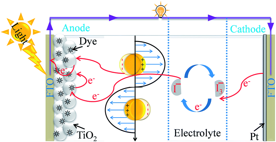

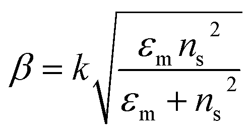
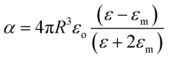
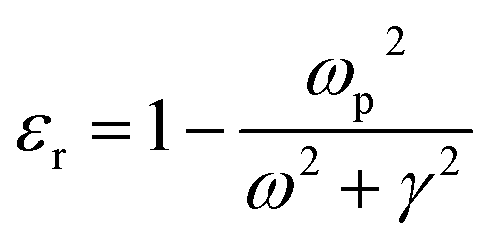
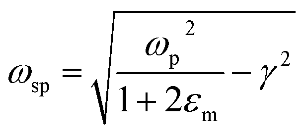
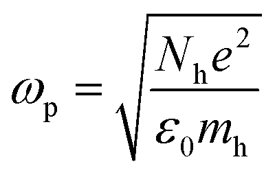
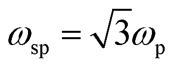 . The order of electron densities for different metals is related to the region of the light spectrum in which resonance occurs. For example, Ag has higher free electron density as compared to Au which results in LSPR in the ultra-violet region for Ag as compared to the visible region for Au.40,41