
 Open Access Article
 This Open Access Article is licensed under a Creative Commons Attribution-Non Commercial 3.0 Unported Licence
Achieving current rectification ratios ≥ 105 across thin films of coordination polymer†
Anupam
Prasoon
 ,
Barun
Dhara
,
Debashree
Roy
,
Shammi
Rana
,
Sujit
Bhand
and
Nirmalya
Ballav
*
,
Barun
Dhara
,
Debashree
Roy
,
Shammi
Rana
,
Sujit
Bhand
and
Nirmalya
Ballav
*
Department of Chemistry, Indian Institute of Science Education and Research (IISER), Dr Homi Bhabha Road, Pashan, Pune 411008, India. E-mail: nballav@iiserpune.ac.in
First published on 5th September 2019
Abstract
Downsizing coordination polymers (CPs) to thin film configurations is a prerequisite for device applications. However, fabrication of thin films of CPs including metal–organic frameworks (MOFs) with reasonable electrical conductivity is challenging. Herein, thin film fabrication of a Cu(II)-CP employing a layer-by-layer method is demonstrated whereby a self-assembled monolayer on Au was used as the functionalized substrate. Growth of the Cu(II)-CP at the solid–liquid interface generated open-metal Cu(II) sites in the thin film which were susceptible to activation by molecular dopant molecules. A significant enhancement in in-plane electrical conductivity and an unheralded cross-plane current rectification ratio (exceeding 105 both at room-temperature and at an elevated temperature) were achieved. Such a remarkable rectification ratio was realized, similar to those of commercial Si rectifier diodes. This phenomenon is attributed to the formation of an electronic heterostructure in the molecularly doped thin film. Molecular doping additionally transformed the interfacial properties of thin films from hydrophilic to highly hydrophobic.
Introduction
Metal–organic frameworks (MOFs) are a unique class of porous materials which have been extensively explored for various promising applications such as gas adsorption and separation, sensors, and catalysis.1,2 However, it was only recently that MOFs were used in the domain of semiconductors,3–6 their limitation primarily being the insulating nature of the organic linker and the poor overlap between their s/p-orbitals and the d-orbitals of the metal ions. Thus, the realization of reasonable electrical conductivity in coordination polymers (CPs) could potentially open the door to the development of electronic and electrochemical devices ranging from chemiresistive sensors, field-effect transistors, light-harvesting devices, fuel cells, supercapacitors, and thermoelectric devices to photovoltaic devices.4 Various approaches to confer electrical conductivity to MOFs include linking metal sites with redox-active linkers, hybridizing them with other conductive media, composite formation with conducting polymers and incorporation of redox-active guest molecules were adopted – as elegantly summarized in recent reviews.4–6Of the aforementioned strategies, the introduction of guest molecules remains convenient for imparting conductivity to an otherwise non-conducting MOF as the pores themselves act as the sites for modulating the electrical transport properties.7–17 Although some molecules have successfully been used as dopants to provide conductivity to MOFs, the 7,7,8,8-tetracyanoquinodimethane (TCNQ) molecule has paved the way to rationally design and enhance the conductivity of such systems by several orders of magnitude.8 A continuous conductivity path between TCNQ and the open-metal sites of binuclear Cu(II) paddle wheels was attributed to the conductivity enhancement by 106 times.8,9 Such thin films of MOFs can be fabricated by various techniques; however, the layer-by-layer (LbL) approach is considered to be the most robust as it not only results in the growth of oriented films of MOFs but is also known for being easily performed and cost-effective.18,19
Herein, we describe for the first time the fabrication of thin films of Cu–BTEC, a Cu(II)-coordination polymer (CP) with the 1,2,4,5-benzenetetracarboxylic acid (BTEC) ligand,20 on a self-assembled monolayer (SAM) template via the LbL technique (Fig. 1). Interestingly, TCNQ molecules could be directly doped into the Cu–BTEC thin film – without the need for activation of the open-metal sites. Doping with TCNQ molecules also leads to a dramatic change in the wetting properties of the Cu–BTEC thin film. A significant enhancement of the in-plane electrical conductivity (six orders of magnitude) of the molecularly doped thin film was detected when the current–voltage (I–V) measurements were performed at 300 K. Remarkably, a current rectification ratio (RR, defined as the absolute value of the quotient between the current recorded for one voltage polarity and the current recorded for the same voltage at the opposite polarity) exceeding 105 was observed when I–V measurements were performed cross-plane which closely matched with the RR values of the commercial diodes 1N4007 and 1N4733A (≥105).
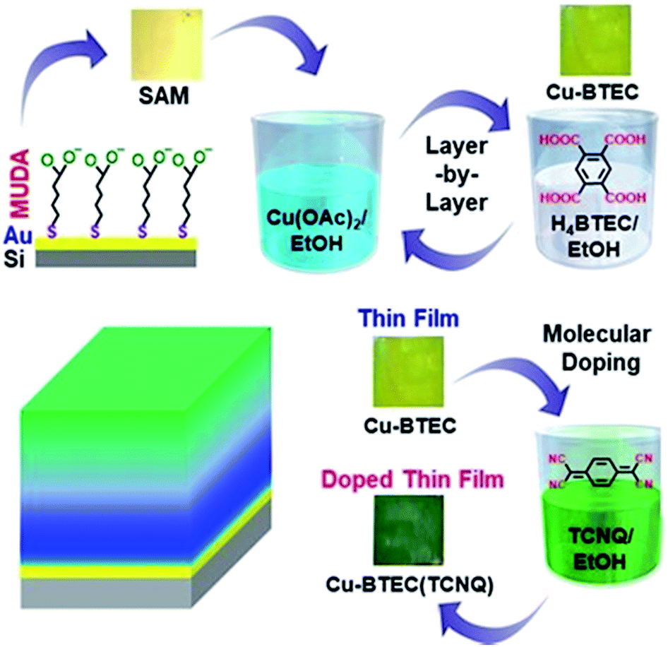 | ||
| Fig. 1 Sequential dipping of the Au-thiolate SAM substrate into Cu(II) acetate and BTEC solutions constitutes one cycle of LbL growth. After 10 growth cycles, molecular doping was performed by soaking the Cu–BTEC thin film into a saturated ethanolic solution of TCNQ for 48 h. A schematic of a molecularly doped thin film of Cu–BTEC. | ||
Commercial diodes (Schottky21 or p–n junctions22) primarily made of inorganic materials, for example Si, have typical RR values in the range of 105–108. However, the best performing molecular diodes23–25 with RR values of 102 to 103 were considered to be inferior to commercial diodes until realization of the ‘supramolecular diode’ at metal/SAM/metal oxide junctions with an RR value beyond 105, driven by electrostatic interactions.26 Also, earlier studies on thin films of MOFs did reveal electrical rectification, specifically at indium tin oxide (ITO)/Cd(II)–MOF/aluminium (Al) junctions;27–30 however, RR values were consistently observed to be <102. Thus, to the best of our knowledge, the present work reports the highest value of RR to date in the domain of organic–inorganic hybrid materials like CPs including MOFs. Furthermore, cross-plane I–V characteristics of our doped thin film at 300 K remained almost unaltered at an elevated temperature of 450 K along with retention of the RR value.
Results and discussion
Fabrication of a thin film sample is schematically depicted in Fig. 1. Briefly, a functionalized Au substrate in the form of a SAM of mercaptoundecanoic acid (MUDA)31 was sequentially dipped into Cu(OAc)2 and BTEC solutions in EtOH to generate a Cu–BTEC thin film via the LbL method19 and the Cu–BTEC thin film was subsequently dipped into a TCNQ solution in EtOH to fabricate the molecularly doped thin film (please refer to the Experimental section for details). Visual inspection of the bare MUDA/Au SAM, after growth of the thin film by the LbL method, and after doping with TCNQ revealed a stark change in colour from golden to yellowish green to dark green (Fig. 1). Specifically, the marked change in colour from the initial yellowish green of the pristine film to the dark green of the doped film was a primary indication of pore filling in Cu–BTEC with TCNQ molecules.8The surface morphologies of pristine and doped Cu–BTEC thin films, as displayed in field-emission scanning electron microscopy (FE-SEM) images, consistently revealed uniform coverage on the Au substrate (Fig. 2a). The insets of FE-SEM images exhibiting the corresponding contact angles (CA) of water clearly showed the conversion from a hydrophilic surface in the pristine film (CA = 15 ± 5°) to a highly hydrophobic surface in the doped film (CA = 135 ± 5°) (Fig. 2a). Apart from the distinctive chemical identity, a notable difference between the surface morphological features of pristine and doped Cu-BTEC thin films is the presence of a reasonably higher number of air-pockets in the latter compared to the former system that could generate highly hydrophobic surfaces32 – as was observed in respective zoomed-in FE-SEM images (Fig. S1†). The thickness of the pristine Cu–BTEC thin film from the cross-sectional FE-SEM image was estimated to be 700 ± 25 nm and this value did not change in the case of the doped Cu–BTEC thin film (Fig. 2a).
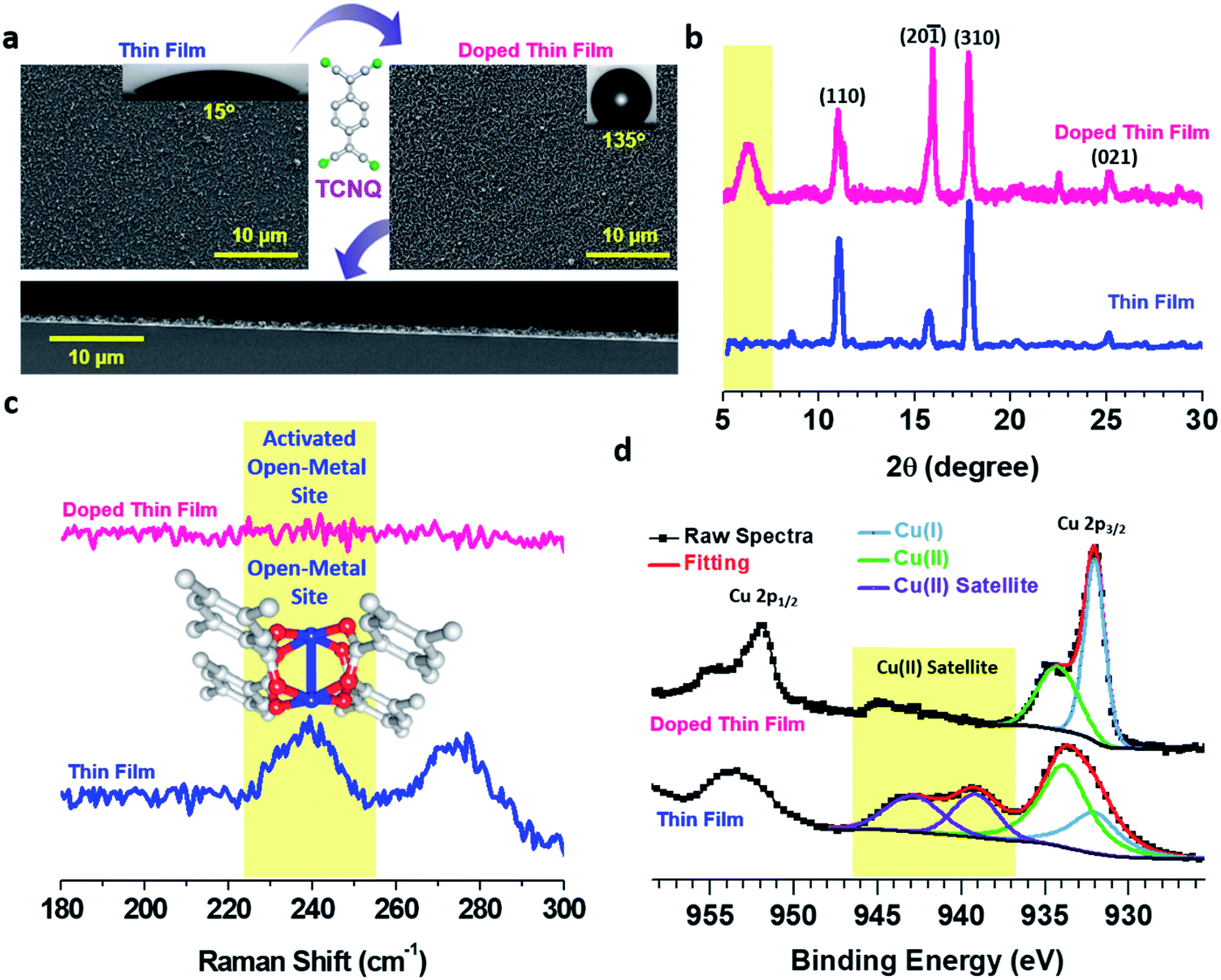 | ||
| Fig. 2 (a) FE-SEM images of pristine and doped Cu–BTEC thin films (inset: optical image of water droplet on the respective surfaces). A cross-sectional FE-SEM image of the doped Cu–BTEC thin film is shown at the bottom. (b) Out-of-plane XRD patterns of pristine (blue) and doped (pink) Cu–BTEC thin films. The characteristic diffraction peak of the pore-filling phenomenon is highlighted in yellow. (c) Raman spectra of pristine (blue) and doped (pink) Cu–BTEC thin films revealing the activation of open-metal sites (characteristic band at ∼240 cm−1 highlighted in yellow) upon doping with TCNQ. (d) High-resolution Cu 2p XPS spectra of pristine (top) and doped (bottom) Cu–BTEC thin films. Satellite spectral zones characteristic of Cu(II) species are highlighted in yellow. | ||
Out-of-plane X-ray diffraction (XRD) patterns of the thin films showed that the crystalline nature of Cu–BTEC20 was retained even after doping with TCNQ molecules (Fig. 2b). The most noticeable change was the appearance of a new peak at 2θ ∼ 5.8° in the case of the doped thin film which can be assigned to the incorporation of TCNQ molecules with an ordering into the Cu–BTEC thin film similar to previous reports on the incorporation of guest molecules into MOFs including thin films.8,11 Note that this new diffraction peak is not characteristic of bulk TCNQ and thus excludes the possibility of TCNQ molecular layers on top of the doped thin film (Fig. S2†). To ensure that our careful washing procedure (after doping) could get rid of additional surface adsorbed TCNQ moieties, we have performed electron paramagnetic resonance (EPR) spectroscopy measurements, and indeed, no characteristic EPR signal of bulk TCNQ at 325 mT (g = 2.00) was observed in the doped thin film (Fig. S3†).8,33
The infiltration of TCNQ into the pores of Cu–BTEC was further demonstrated by Raman measurements wherein a peak at ∼240 cm−1 characteristic of paddle wheel open-metal Cu(II) sites34–36 in the pristine thin film vanished after doping with TCNQ molecules (Fig. 2c). Complete vanishing of the Raman band in the doped thin film could be due to activation of the open-metal sites by TCNQ (top layers) as well as solvent molecules (bottom layers).34 The presence of inherent open-metal sites in the Cu–BTEC thin film helped not only in coordinating the TCNQ molecules to such sites but also in ordering the redox-active guest molecules into the pores of Cu–BTEC. As additional evidence from Raman spectra, we attribute the huge suppression of the C–H out-of-plane bending vibration at 845 cm−1 in the doped film in comparison to the pristine film to the ordering phenomenon (Fig. S4†).37 The solid–liquid interfacial growth of thin films having innate open-metal sites or open-coordination sites is exciting not only in terms of coordinating the incoming guest molecules to the metal centers but also because it eliminates the need for any activation process8,17 which could potentially damage the structural integrity of the framework materials.34,38
The oxidation states of Cu before and after the doping process were probed with the help of high-resolution X-ray photoelectron spectroscopy (XPS). The pristine Cu–BTEC thin film exhibited Cu 2p3/2 signals at ∼934 eV (major) and at ∼932 eV (minor) with strong satellite features indicating the dominant presence of Cu(II) over Cu(I) (Fig. 2d) – consistent with earlier reports on Cu–MOFs obtained from Cu(II) salt and aromatic carboxylic acids.36 However, the doped thin film showed Cu 2p3/2 major signal at ∼932 eV and minor signal at ∼934 eV with an almost complete disappearance of the satellite features thereby confirming that Cu(I) is the dominant species over Cu(II) which were generated upon doping with TCNQ molecules (Fig. 2d).16,39
The bonding motif of TCNQ was investigated by Raman spectroscopy, and upon comparing the Raman spectra of the pristine and doped thin film, a significant red-shift from ∼1455 cm−1 to ∼1374 cm−1 (Δν ∼ 80 cm−1) for the C![[double bond, length as m-dash]](https://www.rsc.org/images/entities/char_e001.gif) C wing stretching mode was observed which suggested charge transfer between the Cu–BTEC framework and TCNQ amounting to ∼1.3e charge for the TCNQ moiety (Fig. S5†).40 The nitrile C
C wing stretching mode was observed which suggested charge transfer between the Cu–BTEC framework and TCNQ amounting to ∼1.3e charge for the TCNQ moiety (Fig. S5†).40 The nitrile C![[triple bond, length as m-dash]](https://www.rsc.org/images/entities/char_e002.gif) N stretching frequency at ∼2208 cm−1 could be fitted with two peaks, one at ∼2202 cm−1 and the other at ∼2217 cm−1, which is an indication that the bonding environment of TCNQ is non-equivalent – two of the CN moieties are bound to the open-metal center while the remaining two CN moieties are unbound (Fig. 3a).8 These findings were substantiated by the infrared reflection-absorption spectroscopy (IRRAS) data which revealed that the CN stretching frequency of the doped film shifted from ∼2223 cm−1 to ∼2202 cm−1 with respect to neutral TCNQ (Fig. S6†) and such a red-shift (Δν ∼ 20 cm−1) can be assigned to partial charge transfer between TCNQ and the Cu–BTEC framework.41 The emergence of characteristic vibrational modes overall provides a strong indication that TCNQ molecules do interact with the open-metal sites available in the Cu–BTEC framework. Furthermore, N 1s XPS data clearly showed two distinct chemical environments, one at a binding energy of ∼398.5 eV and the other at a binding energy of ∼399.5 eV, which can be assigned to bonded and free nitrogens of TCNQ, respectively (Fig. 3b).42,43 Referring to an earlier observation,8 a bonding motif of TCNQ to the Cu–BTEC system is proposed and can be visualized from the schematic in Fig. 3b (an enlarged view is presented in Fig. S7†).
N stretching frequency at ∼2208 cm−1 could be fitted with two peaks, one at ∼2202 cm−1 and the other at ∼2217 cm−1, which is an indication that the bonding environment of TCNQ is non-equivalent – two of the CN moieties are bound to the open-metal center while the remaining two CN moieties are unbound (Fig. 3a).8 These findings were substantiated by the infrared reflection-absorption spectroscopy (IRRAS) data which revealed that the CN stretching frequency of the doped film shifted from ∼2223 cm−1 to ∼2202 cm−1 with respect to neutral TCNQ (Fig. S6†) and such a red-shift (Δν ∼ 20 cm−1) can be assigned to partial charge transfer between TCNQ and the Cu–BTEC framework.41 The emergence of characteristic vibrational modes overall provides a strong indication that TCNQ molecules do interact with the open-metal sites available in the Cu–BTEC framework. Furthermore, N 1s XPS data clearly showed two distinct chemical environments, one at a binding energy of ∼398.5 eV and the other at a binding energy of ∼399.5 eV, which can be assigned to bonded and free nitrogens of TCNQ, respectively (Fig. 3b).42,43 Referring to an earlier observation,8 a bonding motif of TCNQ to the Cu–BTEC system is proposed and can be visualized from the schematic in Fig. 3b (an enlarged view is presented in Fig. S7†).
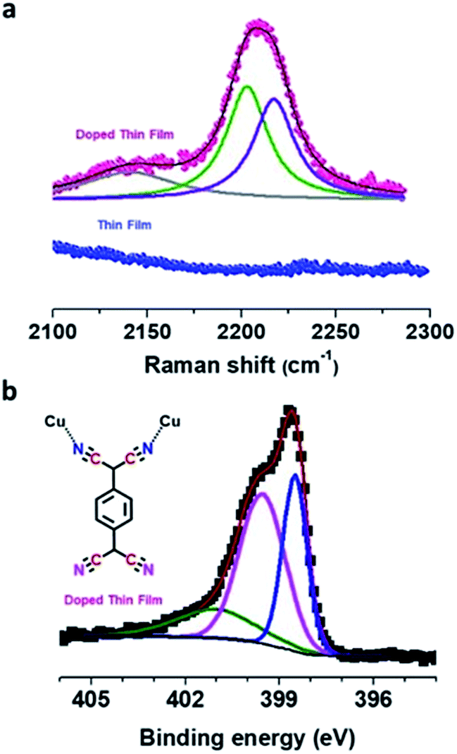 | ||
| Fig. 3 (a) Raman spectra of pristine (blue) and doped (pink) Cu–BTEC thin films. Splitting of the nitrile CN stretching frequency, a feature absent in the pristine thin film, is represented by fitted lines. (b) N 1s XPS spectrum showing two peaks which can be attributed to the distinct chemical environments, bonded (blue) and free (pink) nitrogens of TCNQ, in the doped Cu–BTEC thin film. The green fitted line is assigned to a satellite feature. | ||
The solid-state UV-vis absorption spectra of pristine and doped thin films were markedly different (Fig. 4a) – prominent absorption peaks in the visible region suggested the presence of gap-states in the case of the doped thin film. Such gap-states might reduce the electronic band gap and facilitate electron transport in the thin film.44,45 To investigate the effect of molecular doping on the electrical conductivity, I–V measurements on our thin films were carried out in both in-plane and cross-plane modes. An impressive enhancement (7.8 × 10⁶ times) was observed for the in-plane electrical conductance value of the doped thin film in comparison to that of the pristine thin film (Fig. 4b) resembling electronic coupling between the HKUST-1 MOF (comprising Cu(II) ions and 1,3,5-benzenetricarboxylic acid (BTC) also known as Cu–BTC) and dopant TCNQ generating a conducting path via Cu⋯TCNQ links.8 Poor conductivity of Cu–BTEC could be due to the considerably higher energy level of the lowest unoccupied molecular orbital (LUMO) in comparison to the work function values of standard metallic electrodes; on the other hand, the LUMO level of TCNQ is substantially closer to the Fermi energy of electrodes. In an electronically interacting system of Cu–BTEC and TCNQ, the highest occupied molecular orbital (HOMO)/LUMO levels of Cu–BTEC and TCNQ are expected to be primarily localized in the eg orbitals of Cu centres in the paddle wheel unit and π orbitals, respectively.12 Therefore, an increase in the conductivity value of TCNQ doped Cu–BTEC is expected due to efficient orbital overlap (dx2−y2 → π* and π → dx2−y2) reducing the injection barrier.9
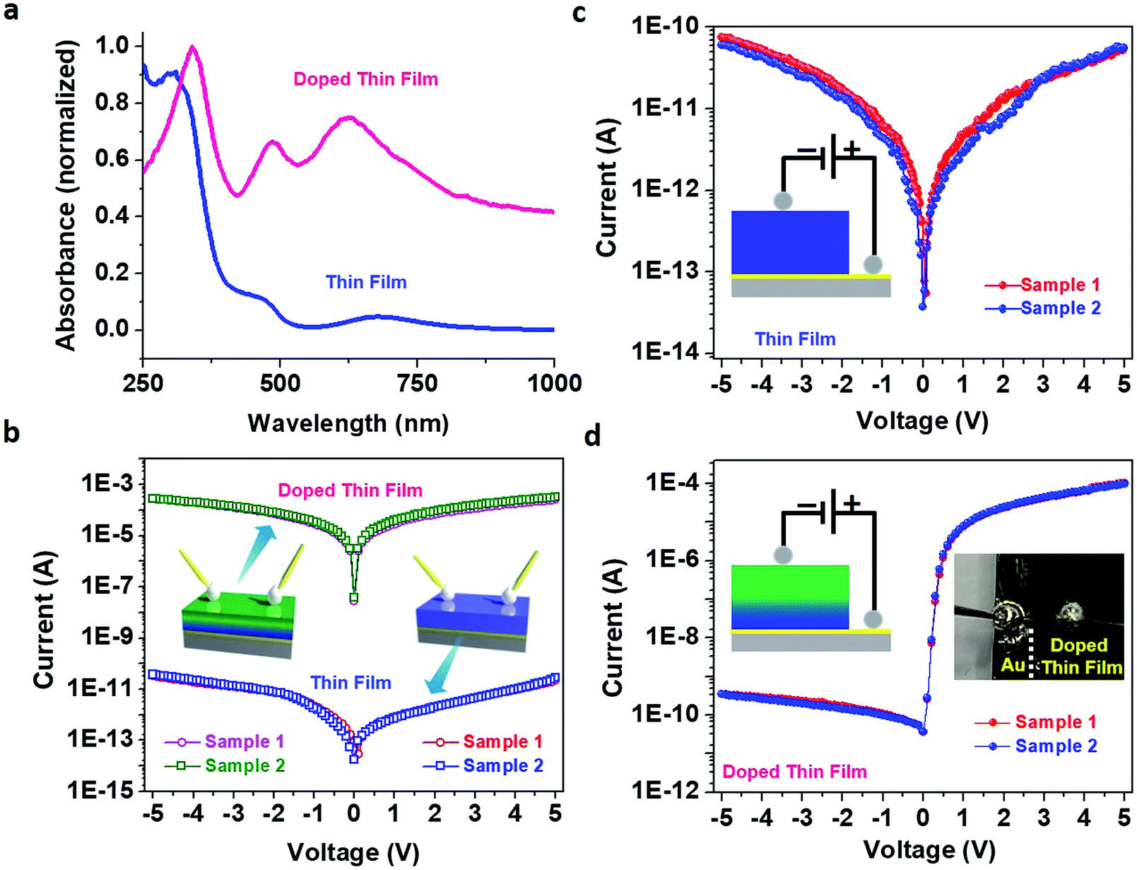 | ||
| Fig. 4 (a) Solid-state UV-vis absorption spectra of pristine (blue) and doped (pink) Cu–BTEC thin films. The presence of prominent absorption peaks in the visible region suggests the existence of gap-states in the doped thin film which were absent in the pristine thin film. (b) In-plane current–voltage (I–V) characteristics of pristine (blue and red) and doped (green and magenta) Cu–BTEC thin films, obtained for two different batches of samples, showing a significant enhancement in the conductivity in the latter. (c) Cross-plane current–voltage (I–V) characteristics of the pristine (red and blue) Cu–BTEC thin film, obtained for two different batches of samples, showing no current rectification. The current direction is illustrated schematically. (d) Cross-plane current–voltage (I–V) characteristics of the doped (blue and red) Cu–BTEC thin film, obtained for two different batches of samples, showing a clear current rectification with an RR value ≥105. Schematics of I–V measurements are shown in the insets of (b) with illustration of the current direction in (c) and (d); a photograph of one representative TCNQ doped Cu–BTEC thin film device is shown in (d) wherein the sample was scratched till Au was visible for the I–V measurements in the cross-plane mode using EGaIn contacts. | ||
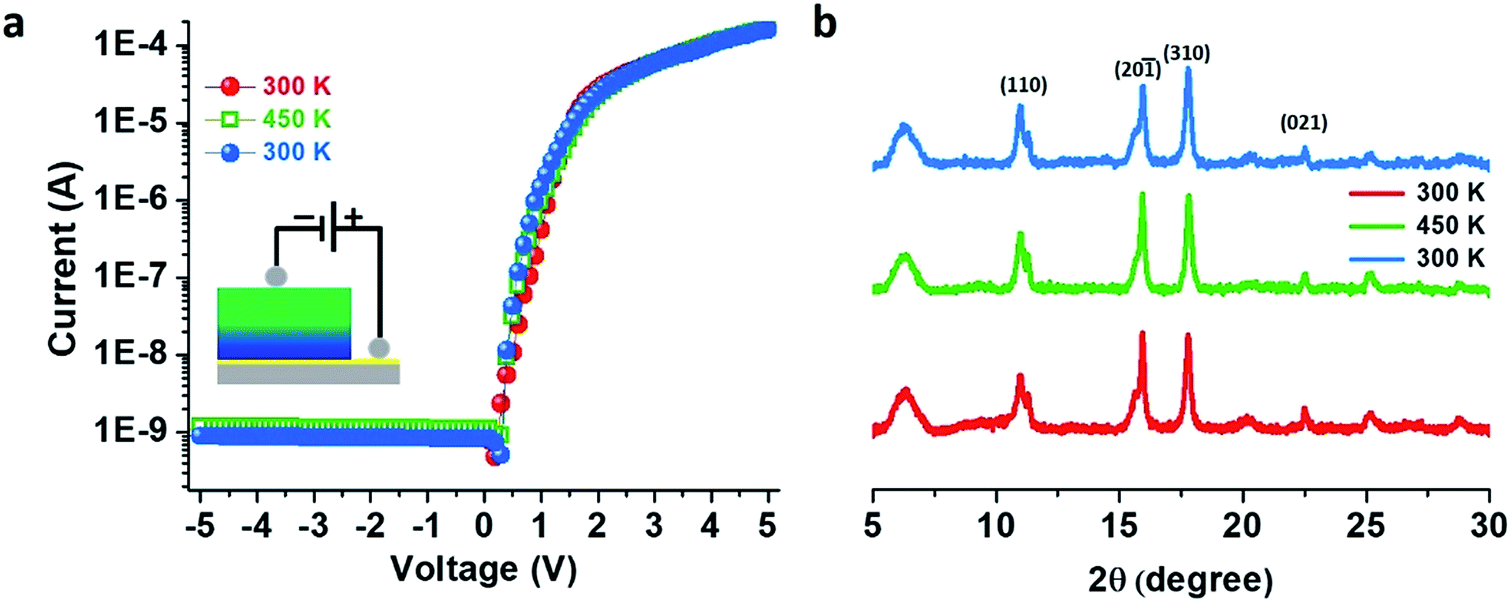
When I–V measurements were carried out in cross-plane mode, the electrical conductance value of the pristine thin film was observed to be similar to the in-plane conductance value (3.6 × 10⁻¹¹ and 6.8 × 10⁻¹¹ S, respectively) (Fig. 4c); interestingly however, a remarkable rectification feature was observed for the doped thin film (Fig. 4d). The RR value was estimated to be more than 105 – a record value in the realm of organic–inorganic hybrid materials as well as coordination polymers. This is a huge achievement considering the fact that coordination polymers including MOFs (either in bulk form or in thin film form) so far have not been able to cross the 102 mark in RR values.27–30 Motivated by such an unusual observation, we wanted to directly compare the I–V characteristics of our system with those of commercial Si diodes (1N4007 and 1N4733A), and RR values were estimated to be on par (Fig. S8†)!
Now the question is, why the unusual rectification of electrical conductivity across molecularly doped thin films? It can be reasoned that formation of an electronic heterostructure occurs under the adopted experimental conditions; for a thin film with a thickness of ∼700 ± 25 nm, only the top layers were doped with the guest molecules while the bottom layers closer to the Au substrate remained pristine due to saturation in the uptake of TCNQ (or a concentration gradient across the thin film).46 In the cross-sectional energy-dispersive X-ray spectroscopy (EDXS) data elemental nitrogen (N) acting as a marker for TCNQ was mainly present in the top layers of the film but was conspicuous by its absence in the bottom layers (Fig. S9†). Thus, while carrying out I–V measurements in-plane, only enhancement of the electrical conductivity was observed; however for I–V measurements performed cross-plane, rectification was observed because the flow of current was restricted due to the electronic heterostructure resembling a typical p–n junction.47,48 So, roughly half of the thin film was conductive while the other half was insulating in nature, giving rise to the rectification. Conventionally, in a p–n junction diode, the positive terminal of the source is connected to the p-type material and the negative terminal of the source is connected to n-type material in forward bias and vice versa in reverse bias.49 In the case of our doped thin film, when we connected the negative terminal of the source to the upper side of the thin film and the positive terminal of the source to the lower side of the thin film, forward bias I–V characteristics (and vice versa in reverse bias) were observed. Knowing the p–n junction identity of commercial Si diodes (1N4007) and complementarity in the I–V characteristics, we can assume that the top and bottom layers of our doped thin film behave like n-type and p-type materials, respectively (Fig. S10†). To further support our claim, we have recorded capacitance–voltage (C–V) characteristics on pristine and doped Cu–BTEC thin films and plotted 1/C2 values vs. V – so called Mott–Schottky analysis (Fig. S11†).50,51 A negative slope for the pristine thin film indicates a p-type material while a positive slope for the doped thin film is typical of an n-type semiconductor.
Schottky barriers at the metal–semiconductor interfaces are well known to cause current rectification and all the previous MOF Schottky diodes were demonstrated to primarily originate from specific semiconducting MOF–metal interfaces.27–30 To check such a possibility in our system, we have measured in-plane and cross-plane I–V characteristics on the doped thin film using various types of contacts, namely EGaIn, conductive C paste, direct Au tips, and direct Pt tips, having different work function values. However, similar I–V patterns as well as RR values were consistently observed (Fig. S12†) which suggested that the CP–metal Schottky contact is not the dominating factor at the origin of such an electrical rectification. Further, we deliberately spin-coated TCNQ on top of a pristine Cu–BTEC thin film and carried out I–V measurements. An enhancement in the in-plane electrical conductance value of the spin-coated thin film in comparison to that of the pristine thin film was observed; interestingly however, no cross-plane electrical rectification was observed (Fig. S13†) thereby clearly demonstrating the fact that even if additional TCNQ moieties are present on the surface of the doped thin film, the TCNQ–CP interface does not cause the electrical rectification. Overall, in the present system of the TCNQ doped Cu–BTEC thin film, the Schottky barrier was apparently a minor factor; rather, formation of a p–n junction type electronic heterostructure was the dominating factor in the current rectification process.
Looking closely at the resistance values obtained in cross-plane mode, it can be seen that the values pertaining to the negative potential correspond very well to those observed for the pristine thin film (∼109) while the values pertaining to the positive potential resemble those of the doped thin film (∼104). This finding also corroborates the presence of an electronic heterostructure in the film. To further verify that the rectification behaviour was due to our chemically engineered thin film and not an instrumental artefact, the directionality of current flow was reversed to source measure unit (SMU)-2 from source measure unit (SMU)-1 (and vice versa), and indeed, a reverse pattern was observed (Fig. S10†). Note also that our I–V data on pristine as well as doped thin films, in both in-plane and cross-plane modes, were successfully reproduced across different batches of samples (Fig. S14†). Also, substrate scope for fabrication of such CP thin films appears flexible.52 The uptake of TCNQ in the thin film as a function of time and the corresponding electrical response could perhaps provide better insight into the microscopic origin of the electronic heterostructure vis-à-vis current rectification.
An activation energy (Ea) of 0.16 eV from the Arrhenius plot was estimated11 from the temperature dependency of the in-plane I–V characteristics for the doped thin film (Fig. S15†). Temperature-dependent I–V measurements in cross-plane mode on the doped thin film showed no appreciable change in the rectification features, and the RR values remained constant at 3.1 × 10⁵ when the temperature was increased to 450 K and again cooled down to 300 K which implies that our thin film as well as the electronic heterostructure is very stable and can sustain temperatures as high as 450 K (Fig. 5a) in agreement with the temperature-dependent PXRD patterns (Fig. 5b) – also a notable achievement in the field of CPs.
 | ||
| Fig. 5 (a) Variable-temperature I–V characteristics of the doped Cu–BTEC thin films recorded at 300 K (red), at 450 K (green) and when cooling back to 300 K (blue). The current direction is illustrated schematically in the inset. (b) Variable-temperature out-of-plane XRD patterns of the doped Cu–BTEC thin film recorded at 300 K (red), at 450 K (green) and when cooling back to 300 K (blue). | ||
A recent report clearly showed the conversion of Cu–BTC to Cu–TCNQ on exposure to a methanolic (protic solvent) TCNQ solution;17 however, no such transformation was observed in the present work. Our various complementary measurements ruling out the possibility of formation of a Cu–TCNQ/Cu–BTEC lattice heterostructure are as follows: (1) the crystalline structure of Cu–BTEC was well-preserved in the doped thin film and the characteristic diffraction peak at 2θ = 5.8° was absent in the pristine Cu–TCNQ thin film (Fig. S16†).32,53 The Raman band of pristine Cu–TCNQ at 520 cm−1 (perhaps due to the Cu⋯Cu interaction mode) was absent in our doped thin film (Fig. S17†). (3) In our EDXS analysis, a uniform presence of elemental oxygen (O) on the surface as well as the cross-section in both pristine and doped thin films was observed (Fig. S18†). (4) In the case of pristine Cu–TCNQ, one main peak in the N 1s XPS signal is expected;54 however, the N 1s XPS spectrum of our doped thin film clearly exhibited two distinctive peaks. (5) The solid-state UV-vis spectra of the pristine Cu–TCNQ thin film and our doped thin film were markedly different (Fig. S19†). (6) Finally, the in-plane I–V characteristics of our doped thin film, both at room-temperature and at high-temperature, were observed to be distinct from those of the pristine Cu–TCNQ thin film (Fig. S20†).32,53
Conclusions
In summary, we have been successful in fabricating a Cu–BTEC thin film on a functionalized Au substrate employing the LbL method. The as-fabricated thin film was found to abound with inherent open-metal Cu(II) sites which guided the ordering of incoming dopant TCNQ molecules in the void space. Such molecular doping created an electronically coupled path leading to a large enhancement in the in-plane electrical conductivity and noticeably modulated water affinity of the thin film from hydrophilic to highly hydrophobic. When I–V measurements were performed in cross-plane mode, an unprecedented current rectification ratio value was observed in our system at room-temperature which was unaltered even at an elevated temperature of 450 K. An electronic (not lattice) heterostructure (p–n junction type) in the molecularly doped thin film was assumed to be at the origin of such an unusual electronic property. We hope that our presented concept will be useful in the development of semiconducting CP-based thin film devices for real-world applications.Experimental
Chemicals
Copper acetate [Cu(OAc)2·H2O], 1,2,4,5-benzenetetracarboxylic acid (BTEC), 7,7,8,8-tetracyanoquinodimethane (TCNQ), the Au substrate (100 nm Au coated on Si wafer), and 11-mercaptoundecanoic acid (MUDA) were purchased from Sigma-Aldrich and used without further purification except for the Au substrate which was cleaned by dipping in Piranha solution (H2SO4 (95–98%)/H2O2 (30%), v/v 3![[thin space (1/6-em)]](https://www.rsc.org/images/entities/char_2009.gif) :1) for 30 minutes followed by washing with Milli-Q water and ethanol and then drying in a stream of N2 gas.
:1) for 30 minutes followed by washing with Milli-Q water and ethanol and then drying in a stream of N2 gas.
Thin film fabrication
A carboxy-terminated (–COOH) SAM was prepared by dipping the Au substrate into a 1 mM solution of MUDA in ethanol/acetic acid (vol/vol = 9:1) for 48 h followed by washing with ethanol and drying under a stream of N2 gas. Cu–BTEC thin films were fabricated by employing the LbL method. The MUDA/Au SAM was immersed into a 1 mM ethanolic solution of Cu(OAc)2·H2O kept at 330 K followed by rinsing with EtOH and drying under a stream of N2 gas. Subsequently, the Cu(II) decorated SAM was dipped into a 1 mM ethanolic solution of BTEC kept at 330 K for 30 min to complete 1 cycle of the LbL method. 10 growth cycles were performed to achieve a film thickness of 700 ± 25 nm. Molecular doping was performed by soaking the Cu–BTEC thin film into a saturated ethanolic solution of TCNQ for 48 h followed by washing with ethanol to remove surface adsorbed TCNQ. The pristine Cu–TCNQ thin film on the MUDA/Au SAM was prepared by using a previously established method in our lab;32 only the temperature was elevated to 330 K for faster growth and to save solvent without compromising the thin film quality.
Characterization
The surface morphology, elemental composition and thickness of pristine and doped Cu–BTEC thin films were analysed with a Zeiss Ultra Plus FE-SEM with an EDXS attachment. Contact angle measurements were carried out using Holmarc's Contact Angle Meter. Out-of-plane XRD data were recorded at room temperature using a Bruker D8 Advance diffractometer using Cu Kα radiation (λ = 1.5406 Å). EPR measurements were performed at room-temperature with the help of a JES – FA200 ESR Spectrometer with X and Q band facilities. Raman spectra (λexc = 633 nm) were recorded using a Raman microscope (LabRAM HR, HorbiaJobinYvon) with a 60× objective lens. High-resolution XPS spectra were recorded using a Scienta R4000 analyser and a monochromatic Al Kα source. The instrumental energy resolution was 0.3 eV. Transmission lens mode was used and the pass energy was set to 100 eV. Infrared Reflection Absorption Spectroscopy (IRRAS) measurements were performed on a Cary 600 Series FTIR (Agilent Technologies) spectrometer coupled with a microscope. Solid state UV-vis absorption spectra were recorded on Shimadzu UV 3600 UV-Vis-NIR spectrophotometer. Capacitance–voltage (C–V) plots on pristine and doped thin films were recorded in PARSTAT MC PMC-2000 instrument. Electrical transport measurements (I–V) on various thin film samples were carried out using a Keithley 4200 SCS Parameter Analyser system attached to an Everbeing probe station (equipped with a thermal chuck) with a eutectic gallium indium (EGaIn) alloy as the top electrode.53Author contributions
A. P. planned the experimental sessions and performed most of the experiments. B. D. performed XPS and additional I–V measurements. D. R., S. R. and S. B. took part in sample preparation, characterization, I–V measurements and data analysis. N. B. conceived and supervised the research project and wrote the manuscript with input from D. R.Conflicts of interest
There are no conflicts to declare.Acknowledgements
Financial support from the SERB (India, Project No. EMR/2016/001404), MHRD-FAST (India, Project CORESUM), and IISER Pune is thankfully acknowledged. A. P. acknowledges the DST-KVPY for a student fellowship. B. D. and S. B. thank the SERB (India, Project No. EMR/2016/001404) for a research fellowship. D. R. and S. R. thank IISER Pune for research fellowships. The authors thank SAIF-IIT Mumbai (India) for use of the EPR facility.Notes and references
- A. Bétard and R. A. Fischer, Chem. Rev., 2012, 112, 1055–1083 CrossRef PubMed.
- H. Furukawa, K. E. Cordova, M. O'Keeffe and O. M. Yaghi, Science, 2013, 341, 1230444 CrossRef PubMed.
- S. Takaishi, M. Hosoda, T. Kajiwara, H. Miyasaka, M. Yamashita, Y. Nakanishi, Y. Kitagawa, K. Yamaguchi, A. Kobayashi and H. Kitagawa, Inorg. Chem., 2009, 48, 9048–9050 CrossRef CAS PubMed.
- L. Sun, M. G. Campbell and M. Dincă, Angew. Chem., Int. Ed., 2016, 55, 3566–3579 CrossRef CAS PubMed.
- M. Usman, S. Mendiratta and K.-L. Lu, Adv. Mater., 2017, 29, 1605071 CrossRef PubMed.
- S. K. Bhardwaj, N. Bhardwaj, R. Kaur, J. Mehta, A. L. Sharma, K.-H. Kim and A. Deep, J. Mater. Chem. A, 2018, 6, 14992–15009 RSC.
- Y. Kobayashi, B. Jacobs, M. D. Allendorf and J. R. Long, Chem. Mater., 2010, 22, 4120–4122 CrossRef CAS.
- A. A. Talin, A. Centrone, A. C. Ford, M. E. Foster, V. Stavila, P. Haney, R. A. Kinney, V. Szalai, F. El Gabaly and H. P. Yoon, Science, 2014, 343, 66–69 CrossRef CAS PubMed.
- M. D. Allendorf, M. E. Foster, F. Leonard, V. Stavila, P. L. Feng, F. P. Doty, K. Leong, E. Y. Ma, S. R. Johnston and A. A. Talin, J. Phys. Chem. Lett., 2015, 6, 1182–1195 CrossRef CAS PubMed.
- J. Liu, T. Wächter, A. Irmler, P. G. Weidler, H. Gliemann, F. Pauly, V. Mugnaini, M. Zharnikov and C. Wöll, ACS Appl. Mater. Interfaces, 2015, 7, 9824–9830 CrossRef CAS PubMed.
- B. Dhara, S. S. Nagarkar, J. Kumar, V. Kumar, P. K. Jha, S. K. Ghosh, S. Nair and N. Ballav, J. Phys. Chem. Lett., 2016, 7, 2945–2950 CrossRef CAS PubMed.
- T. Neumann, J. Liu, T. Wächter, P. Friederich, F. Symalla, A. Welle, V. Mugnaini, V. Meded, M. Zharnikov, C. Wöll and W. Wenzel, ACS Nano, 2016, 10, 7085–7093 CrossRef CAS PubMed.
- Z. Guo, D. K. Panda, K. Maity, D. Lindsey, T. G. Parker, T. E. Albrecht-Schmitt, J. L. Barreda-Esparza, P. Xiong, W. Zhou and S. Saha, J. Mater. Chem. C, 2016, 4, 894–899 RSC.
- B. Le Ouay, M. Boudot, T. Kitao, T. Yanagida, S. Kitagawa and T. Uemura, J. Am. Chem. Soc., 2016, 138, 10088–10091 CrossRef CAS PubMed.
- T. Wang, M. Farajollahi, S. Henke, T. Zhu, S. R. Bajpe, S. Sun, J. S. Barnard, J. S. Lee, J. D. W. Madden, A. K. Cheetham and S. K. Smoukov, Mater. Horiz., 2017, 4, 64–71 RSC.
- C. Schneider, D. Ukaj, R. Koerver, A. A. Talin, G. Kieslich, S. P. Pujari, H. Zuilhof, J. Janek, M. D. Allendorf and R. A. Fischer, Chem. Sci., 2018, 9, 7405–7412 RSC.
- K. Thürmer, C. Schneider, V. Stavila, R. W. Friddle, F. o. Léonard, R. A. Fischer, M. D. Allendorf and A. A. Talin, ACS Appl. Mater. Interfaces, 2018, 10, 39400–39410 CrossRef PubMed.
- R. Makiura, S. Motoyama, Y. Umemura, H. Yamanaka, O. Sakata and H. Kitagawa, Nat. Mater., 2010, 9, 565 CrossRef CAS PubMed.
- J.-L. Zhuang, A. Terfort and C. Wöll, Coord. Chem. Rev., 2016, 307, 391–424 CrossRef CAS.
- H. K. Zhao, B. Ding, E. C. Yang, X. G. Wang and X. J. Zhao, Z. Anorg. Allg. Chem., 2007, 633, 1735–1738 CrossRef CAS.
- R. T. Tung, Mater. Sci. Eng., R, 2001, 35, 1–138 CrossRef.
- P. A. Beck, J. H. Nickel and P. G. Hartwell, MRS Proceedings, 2004, 808, A–4.30 CrossRef.
- B. Capozzi, J. Xia, O. Adak, E. J. Dell, Z.-F. Liu, J. C. Taylor, J. B. Neaton, L. M. Campos and L. Venkataraman, Nat. Nanotechnol., 2015, 10, 522 CrossRef CAS PubMed.
- L. Yuan, R. Breuer, L. Jiang, M. Schmittel and C. A. Nijhuis, Nano Lett., 2015, 15, 5506–5512 CrossRef CAS PubMed.
- M. L. Perrin, E. Galán, R. Eelkema, J. M. Thijssen, F. Grozema and H. S. J. van der Zant, Nanoscale, 2016, 8, 8919–8923 RSC.
- X. Chen, M. Roemer, L. Yuan, W. Du, D. Thompson, E. del Barco and C. A. Nijhuis, Nat. Nanotechnol., 2017, 12, 797 CrossRef CAS PubMed.
- S. Dalapati, R. Saha, S. Jana, A. K. Patra, A. Bhaumik, S. Kumar and N. Guchhait, Angew. Chem., Int. Ed., 2012, 51, 12534–12537 CrossRef CAS PubMed.
- B. Bhattacharya, A. Layek, M. M. Alam, D. K. Maity, S. Chakrabarti, P. P. Ray and D. Ghoshal, Chem. Commun., 2014, 50, 7858–7861 RSC.
- S. Halder, A. Dey, A. Bhattacharjee, J. Ortega-Castro, A. Frontera, P. P. Ray and P. Roy, Dalton Trans., 2017, 46, 11239–11249 RSC.
- S. Roy, M. Das, A. Bandyopadhyay, S. K. Pati, P. P. Ray and T. K. Maji, J. Phys. Chem. C, 2017, 121, 23803–23810 CrossRef CAS.
- R. Arnold, W. Azzam, A. Terfort and C. Wöll, Langmuir, 2002, 18, 3980–3992 CrossRef CAS.
- S. Rana, R. Rajendra, B. Dhara, P. K. Jha and N. Ballav, Adv. Mater. Interfaces, 2016, 3, 1500738 CrossRef.
- J. Mahmood, J. Park, D. Shin, H.-J. Choi, J.-M. Seo, J.-W. Yoo and J.-B. Baek, Chem, 2018, 4, 2357–2369 CAS.
- H. K. Kim, W. S. Yun, M.-B. Kim, J. Y. Kim, Y.-S. Bae, J. Lee and N. C. Jeong, J. Am. Chem. Soc., 2015, 137, 10009–10015 CrossRef CAS PubMed.
- J. S. Choi, J. Bae, E. J. Lee and N. C. Jeong, Inorg. Chem., 2018, 57, 5225–5231 CrossRef CAS PubMed.
- A. S. Duke, E. A. Dolgopolova, R. P. Galhenage, S. C. Ammal, A. Heyden, M. D. Smith, D. A. Chen and N. B. Shustova, J. Phys. Chem. C, 2015, 119, 27457–27466 CrossRef CAS.
- N. R. Dhumal, M. P. Singh, J. A. Anderson, J. Kiefer and H. J. Kim, J. Phys. Chem. C, 2016, 120, 3295–3304 CrossRef CAS.
- M. K. Bhunia, J. T. Hughes, J. C. Fettinger and A. Navrotsky, Langmuir, 2013, 29, 8140–8145 CrossRef CAS PubMed.
- S. Rana, A. Prasoon, P. Sadhukhan, P. K. Jha, V. Sathe, S. R. Barman and N. Ballav, J. Phys. Chem. Lett., 2018, 9, 6364–6371 CrossRef CAS PubMed.
- S. Matsuzaki, R. Kuwata and K. Toyoda, Solid State Commun., 1980, 33, 403–405 CrossRef CAS.
- J. Chappell, A. Bloch, W. Bryden, M. Maxfield, T. Poehler and D. Cowan, J. Am. Chem. Soc., 1981, 103, 2442–2443 CrossRef CAS.
- R. Precht, R. Hausbrand and W. Jaegermann, Phys. Chem. Chem. Phys., 2015, 17, 6588–6596 RSC.
- C. Wäckerlin, C. Iacovita, D. Chylarecka, P. Fesser, T. A. Jung and N. Ballav, Chem. Commun., 2011, 47, 9146–9148 RSC.
- B. Dhara, V. Kumar, K. Gupta, P. K. Jha and N. Ballav, ACS Omega, 2017, 2, 4488–4493 CrossRef CAS PubMed.
- J. Liu, W. Zhou, J. Liu, I. Howard, G. Kilibarda, S. Schlabach, D. Coupry, M. Addicoat, S. Yoneda and Y. Tsutsui, Angew. Chem., Int. Ed., 2015, 54, 7441–7445 CrossRef CAS PubMed.
- L. Heinke, Z. Gu and C. Wöll, Nat. Commun., 2014, 5, 4562 CrossRef CAS PubMed.
- A. Kudo, H. Yanagi, K. Ueda, H. Hosono, H. Kawazoe and Y. Yano, Appl. Phys. Lett., 1999, 75, 2851–2853 CrossRef CAS.
- S. Jung, S. Jeon and K. Yong, Nanotechnology, 2010, 22, 015606 CrossRef PubMed.
- A. Malvino and D. J. Bates, Electronic Principles, McGraw-Hill Education (India) Pvt. Ltd., Chennai, 2007 Search PubMed.
- P. Schmuki, H. Böhni and J. A. Bardwell, J. Electrochem. Soc., 1995, 142, 1705–1712 CrossRef CAS.
- A. Nigam, M. Premaratne and P. R. Nair, Org. Electron., 2013, 14, 2902–2907 CrossRef CAS.
- J.-L. Zhuang, D. Ar, X.-J. Yu, J.-X. Liu and A. Terfort, Adv. Mater., 2013, 25, 4631–4635 CrossRef CAS PubMed.
- S. Rana, A. Prasoon, P. K. Jha, A. Prathamshetti and N. Ballav, J. Phys. Chem. Lett., 2017, 8, 5008–5014 CrossRef CAS PubMed.
- M. J. Capitán, J. Alvarez and F. Yndurain, Phys. Chem. Chem. Phys., 2018, 20, 21705–21715 RSC.
Footnote |
| † Electronic supplementary information (ESI) available. See DOI: 10.1039/c9sc03733k |
| This journal is © The Royal Society of Chemistry 2019 |