
 Open Access Article
 This Open Access Article is licensed under a Creative Commons Attribution-Non Commercial 3.0 Unported Licence
Photoelectric effect accelerated electrochemical corrosion and nanoimprint processes on gallium arsenide wafers
Chengxin
Guo
a,
Lin
Zhang
a,
Matthew M.
Sartin
a,
Lianhuan
Han
*b,
Zhao-Wu
Tian
a,
Zhong-Qun
Tian
 a and
Dongping
Zhan
*a
a and
Dongping
Zhan
*a
aState Key Laboratory of Physical Chemistry of Solid Surfaces (PCOSS), Collaborative Innovation Center of Chemistry for Energy Materials (iChEM), Engineering Research Center of Electrochemical Technologies of Ministry of Education, Department of Chemistry, College of Chemistry and Chemical Engineering, Xiamen University, Xiamen 361005, China. E-mail: dpzhan@xmu.edu.cn
bDepartment of Mechanical and Electrical Engineering, School of Aerospace Engineering, Xiamen University, Xiamen 361005, China
First published on 7th May 2019
Abstract
Here we report photoelectric-effect-enhanced interfacial charge transfer reactions. The electrochemical corrosion rate of n-type gallium arsenide (n-GaAs) induced by the contact potential at platinum (Pt) and GaAs boundaries can be accelerated by the photoelectric effect of n-GaAs. When a GaAs wafer is illuminated with a xenon light source, the electrons in the valence band of GaAs will be excited to the conduction band and then move to the Pt boundaries due to the different work functions of the two materials. This results in an enhanced contact electric field as well as an enlarged Pt/GaAs contact potential. Consequently, in the presence of electrolyte solution, the polarizations of both the Pt/solution interface and the GaAs/solution interface at the Pt/GaAs/solution 3-phase boundary are enhanced. If the accumulated electrons on the Pt side are removed by electron acceptors in the solution, anodic corrosion of GaAs will be accelerated strictly along the Pt/GaAs/solution 3-phase boundary. This photo-enhanced electrochemical phenomenon can increase the corrosion rate of GaAs and accelerate the process of electrochemical nanoimprint lithography (ECNL) on GaAs. The method opens an innovative, highly efficient, low-cost nanoimprint technique performed directly on semiconductors, and it has prospective applications in the semiconductor industry.
Introduction
Electrochemical corrosion is an electrochemical reaction which occurs spontaneously in a “short-circuit” electrolytic microcell.1–4 It is reported that one third of the world's steel products are corroded each year.5 Therefore, a significant effort has been made to develop anti-corrosion technology. On the other hand, corrosion plays an important role in the fabrication of three dimensional micro–nano structures (3D-MNSs) acting as sensors and actuators in microelectromechanical systems (MEMSs) and miniaturized total analysis systems (μ-TASs). Once corrosion processes are well controlled, these could become a competitive template-forming method for the fabrication of 3D MNSs.6,7The original motivation for template forming based on chemical principles is to make large-area 3D-MNSs directly on semiconductor wafers, which is difficult for photolithography and nanoimprint lithography (NIL).8,9 Derived from the mechanical extrusion-forming technique, NIL is considered to be one of the most competitive template-forming microfabrication methods, with high resolution and low cost.10 In general, NIL involves thermoplastic or photocuring resists, which are filled into NIL templates with 3D-MNSs. After demoulding, the 3D-MNSs in the NIL template left in the resists are transferred to functional materials by subsequent technical processes, e.g., physical or chemical etching.11–16 In 2002 laser-assisted direct imprint (LADI) was proposed to fabricate 3D-MNSs on a silicon (Si) wafer. An extremely powerful laser pulse was introduced through a quartz imprint template to melt the Si surface. Simultaneously, high pressure was applied to press the 3D-MNSs into the molten Si surface.17 LADI is very costly, because the laser light source is very expensive and semiconductor wafers are fragile. Direct nanoimprint on semiconductors has seldom been reported since then. Compared to physical methods, template forming methods based on chemical principles are a reasonable choice.
For years we have been engaged in the study of the confined etchant layer technique (CELT) to fabricate functional 3D-MNSs on various semiconductor wafers, where the electrogenerated etchant is confined in a diffusion layer at the micro–nano meter scale.18–20 To avoid the alignment problem of CELT, we recently proposed electrochemical nanoimprint lithography (ECNL) based on contact-potential-induced corrosion.21–23 We found that, when a platinum (Pt) metalized template contacts Si or gallium arsenide (GaAs), a contact potential will be established at the Pt/GaAs boundary, due to the different electronic work functions of the two materials. In the presence of electrolyte solution with electron acceptors, the excess electrons at the Pt side will be transferred across the Pt/solution interface, and the Si or GaAs/solution interface will be polarized and corroded by the accumulated holes strictly along the Pt/semiconductor/solution 3-phase boundaries. Compared with NIL, ECNL works directly on the semiconductor wafer, without any resists or auxiliary processes. The machining accuracy of ECNL is lower than the Debye length of the space charge layer across the Pt/semiconductor boundaries, which means that it is indeed spatially confined corrosion at the micro–nanometer scale.
Here we report that contact-potential-induced corrosion can be accelerated because of the photoelectric effect of the semiconductor substrate. The photo illumination can increase the contact potential between the Pt/GaAs boundaries and thus, enhance the polarization of both the GaAs/solution interface and the Pt/solution interface, resulting in an accelerated anodic dissolution of GaAs. Based on this principle, we demonstrate that the efficiency of ECNL can be promoted by the photo-enhanced electrochemical mechanism.
Results and discussion
When GaAs contacts Pt, electrons will move from n-GaAs to Pt until the Fermi levels of both are equal to one another, because the electron work function of n-GaAs is lower than that of Pt. Consequently, a contact electric field, as well as a contact potential, will be established at the Pt/n-GaAs boundary, in which the Pt side is negatively charged, and the n-GaAs side is positively charged. We have demonstrated that the contact potential can induce the anodic dissolution of n-GaAs (Fig. 1a) when the system is immersed in an electrolyte with electron acceptors (e.g., KMnO4−), and we developed an ECNL technique for the template forming of 3D-MNSs. We realized that n-GaAs is a semiconductor with excellent photoelectric properties. As shown in Fig. 1b, when n-GaAs is illuminated, the electrons will be exited from the valence band to the conduction band, and they will then move to the Pt side, due to the difference in the work functions of the two materials. The system will equilibrate when both materials have the same Fermi level at the Pt/n-GaAs boundary, i.e., to establish thermodynamic equilibrium. The contact potential will be enlarged and the polarizations of both the n-GaAs/solution interface and the Pt/solution interface will be enhanced. Since the kinetic rate of MnO4− reduction on the Pt surface is much higher, the polarization of the GaAs/solution interface will be enhanced, and the anodic corrosion of n-GaAs will be accelerated as depicted in Fig. 1c.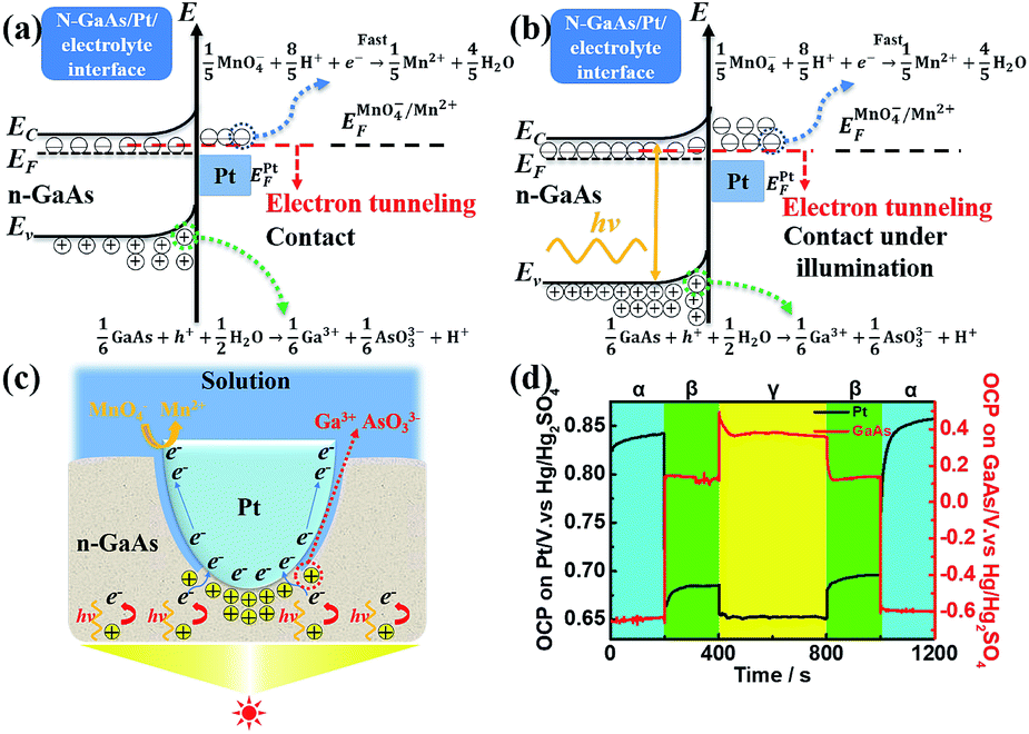 | ||
| Fig. 1 (a) The principle of contact-potential-induced corrosion of n-GaAs. (b) The principle of contact-potential-induced corrosion of n-GaAs enhanced by the photoelectric effect. (c) The schematic diagram of the photoelectric effect accelerated ECNL processes on an n-GaAs wafer. (d) The potential measurements of the Pt/solution interface (black line) and the n-GaAs/solution interface (red line). The α, β, and γ regions correspond to the case where the n-GaAs wafer and the Pt template are separated, contacted without illumination, and contacted with illumination. | ||
The above theoretical analysis is demonstrated experimentally by measurements of interfacial potential in the presence of electrolyte solution with 40 mM KMnO4 and 1.84 M H2SO4. We used a bipotentiostat to monitor the potentials of both the Pt/GaAs interface and the GaAs/solution interface at the same time. As shown in Fig. 1d, when the Pt-metalized template electrode is separated from the GaAs wafer, the potentials of the Pt/GaAs interface and GaAs/solution interface are measured to be 0.84 V and −0.65 V, respectively vs. the Hg/Hg2SO4 reference electrode. When the materials came in contact with each other under a pressure of 0.5 atm, the potential of the Pt/solution interface quickly steps to 0.66 V and finally stabilizes at 0.68 V. Meanwhile, the potential of the GaAs/solution interface increases to 0.13 V, and finally stabilizes at 0.14 V after a transient time. Furthermore, when the back of the GaAs wafer is illuminated with a xenon light source (output power: 460 mW), the potential of the Pt/solution interface decreases from 0.68 V to 0.65 V, and the potential of the GaAs/solution interface increases from 0.13 V to 0.49 V, before stabilizing at 0.38 V. The observed transient state of the GaAs/solution interface from 0.49 V to 0.38 V indicates the establishment of a new thermodynamic equilibrium caused by photo-illumination. All the results show that the photoelectric effect will enhance the polarization of both the Pt/solution interface and the GaAs/solution interface. The processes are very reversible when light illumination is stopped and when the Pt template is separated from the GaAs wafer (Fig. 1d).
How does the photoelectric-effect-enhanced polarization affect the interfacial charge transfer reaction? Linear scan voltammetry experiments were performed separately using the Pt electrode and the GaAs electrode without and with illumination in the same electrolyte solution. The area of the n-GaAs electrode and Pt disk electrode is 1.5 cm2 and 0.0314 cm2, respectively. As shown in Fig. 2a and b, the apparent anodic current density on the GaAs electrode is about 6.7 μA cm−2 without illumination and increases to more than 77.9 μA cm−2 with illumination. The current density change on the Pt electrode is not so dramatic, but it is still much higher than that obtained on the GaAs electrode (Fig. 2c and d). Fig. 3 and Table 1 show the Tafel experiments and the calculated kinetic parameters, indicating that the exchange current density (i0) of the anodic corrosion of GaAs increases from (6.42 × 10⁻¹⁰) A cm−2, in the dark, to (2.68 × 10⁻⁷) A cm−2, under illumination. However, the i0 of MnO4− reduction on the Pt electrode increases from (5.16 × 10⁻⁴) A cm−2, in the dark, to (7.42 × 10⁻⁴) A cm−2, under illumination. From the i0 values, it can be concluded that the cathodic reduction rate of MnO4− on the Pt electrode is still much higher than the anodic corrosion rate of GaAs even under illumination. The rate-determining step of the reaction system is the corrosion of GaAs, regardless of whether or not the system is illuminated. It should be noted that the corrosion rate of GaAs is promoted by about three orders of magnitude by the photoelectric effect, which indicates acceleration of the ECNL processes and thus an improvement of its fabrication efficiency.
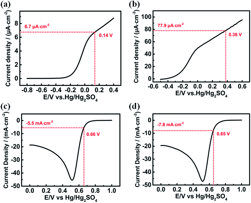 | ||
| Fig. 2 Linear scan voltammograms of the n-GaAs electrode and Pt electrode at a scan rate of 100 mV s−1: (a) and (c) in the dark; (b) and (d) under illumination. The aqueous solution contains 40 mM KMnO4 and 1.84 M H2SO4. The working temperature is kept at 25 °C and the illumination power is 460 mW. | ||
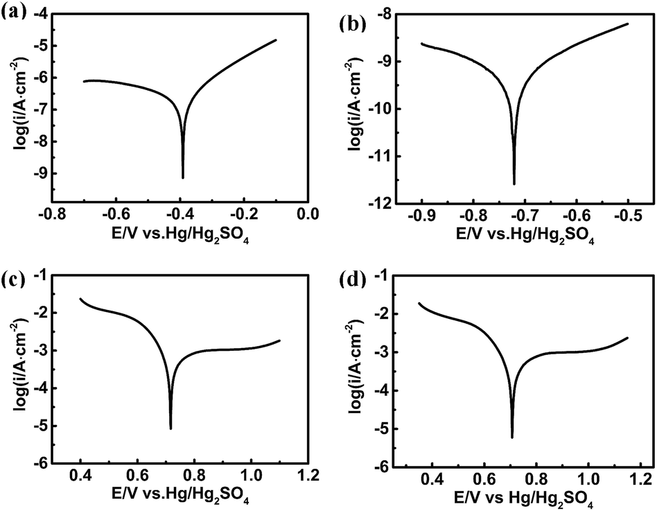 | ||
| Fig. 3 (a), (b) Tafel curves measured on an n-GaAs electrode with and without illumination. (c), (d) Tafel curves measured on a Pt disk electrode with and without illumination. The aqueous solution contains 40 mM KMnO4 and 1.84 M H2SO4. The working temperature is kept at 25 °C and the illumination power is 460 mW. | ||
| E corr (V) | i corr (A cm−2) | Slope | αn | i 0 (A cm−2) | |
|---|---|---|---|---|---|
| a E corr is the corrosion potential, icorr is the corrosion current density, α is the charge transfer coefficient, n is the number of transferred electrons and i0 is the exchange current density. | |||||
| GaAs-dark | −0.714 | 6.87 × 10⁻¹⁰ | 0.217 | 0.272 | 6.42 × 10⁻¹⁰ |
| GaAs-illuminated | −0.394 | 2.68 × 10⁻⁷ | 0.159 | 0.372 | 2.68 × 10⁻⁷ |
| Pt-dark | 0.715 | 5.22 × 10⁻⁴ | −0.144 | 0.410 | 5.16 × 10⁻⁴ |
| Pt-illuminated | 0.729 | 7.44 × 10⁻⁴ | −0.138 | 0.429 | 7.42 × 10⁻⁴ |
Comparison ECNL experiments were performed with and without illumination. Fig. 4a and b show a concave microlens array fabricated by ECNL on a GaAs wafer for a working time of 20 minutes, without and with an illumination power of 460 mW. From the profiles shown in Fig. 4c, it can be seen that the removal rate with illumination is accelerated by more than a factor of 1.5. The dependence of the removal amount on the corrosion time is shown in Fig. 4d. The removal rate will increase rapidly at the beginning and then slow down. Fig. 5a and b show the microlens profiles and removal amount at different illumination powers within 15 minutes. The removal rate (or volume) is improved when the illumination power is higher than 150 mW. This threshold value is actually the balance between the charge separation, recombination, and transport in the n-GaAs wafer, and also the interfacial charge transfer processes involved in ECNL. The removal rate increases linearly with illumination power when the power is higher than the threshold value.
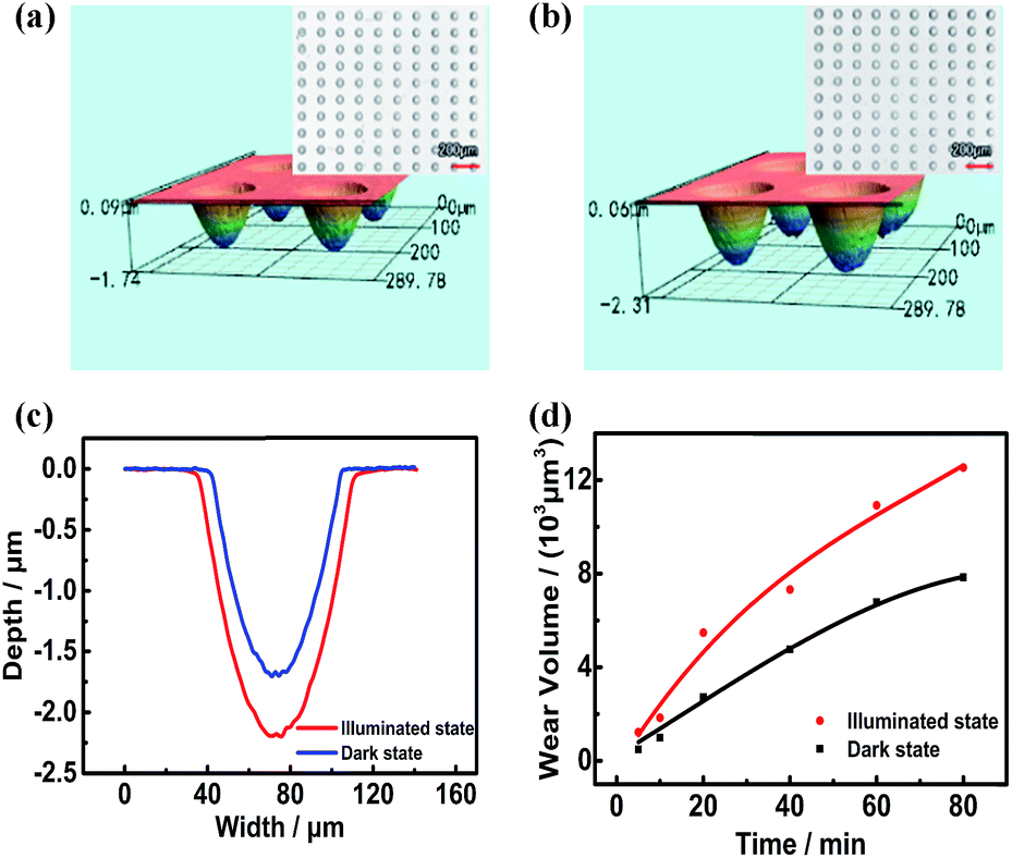 | ||
| Fig. 4 Confocal laser scanning microscope images of structures on n-GaAs fabricated by electrochemical nanoimprint lithography (a) in the dark and (b) under illumination. (c) Comparison of cross-sectional profiles of structures on n-GaAs fabricated under illumination and in the dark. The time is 20 minutes. (d) Relationship between the imprint time and the wear volumes under illumination and in the dark. The aqueous solution contains 40 mM KMnO4 and 1.84 M H2SO4. The working temperature is kept at 25 °C and the illumination power is 460 mW. | ||
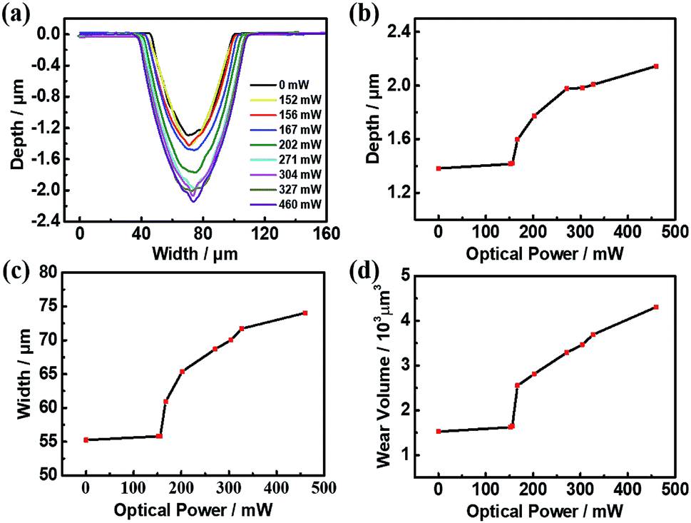 | ||
| Fig. 5 (a) Cross-sectional profiles, (b) depths, (c) widths, and (d) removal volumes of the concave microlens fabricated on an n-GaAs wafer under different illumination powers. The imprint time is 15 minutes, and the aqueous solution contains 40 mM KMnO4 and 1.84 M H2SO4. | ||
From the Tafel experiments performed in the bulk solution with isolated n-GaAs electrodes, we know that the corrosion rate is enhanced by three orders of magnitude with illumination. However, the removal rate of ECNL is not promoted so fast. Indeed, the ECNL system is an isolated, thin-layer electrolytic cell. The rapid consumption of MnO4− anions creates a serious mass balance problem. The decrease of MnO4− concentration will slow down the electron transfer rate on the Pt side. According to the electroneutrality principle, the corrosion rate of n-GaAs by holes will decrease. Although the reduction of MnO4− anions on the Pt electrode is pH-dependent, the consumption of protons will not hinder the electron transfer path, because the proton concentration is more than 90 times higher than that of MnO4− anions.
Experimental
Chemicals and materials
All the chemicals were of analytical grade or better. Potassium permanganate (KMnO4), sulfuric acid (H2SO4), ferrous sulfate (FeSO4·7H2O), hydrogen peroxide (H2O2), ethanol, and acetone were provided by Sinopharm, China. Silicon-doped n-GaAs (100) wafers with a doping level between (0.8–2.3) × 1018 cm−3 were purchased from China Crystal Technologies Co., China. Before the experiments, the n-GaAs wafers were rinsed with acetone, ethanol, and deionized water. The platinum (purity: 99.95%) and titanium (purity: 99.95%) sputtering targets used for the preparation of the ECNL template were provided by the Beijing Cuibolin Nonferrous Metals Institute. All aqueous solutions were prepared with deionized water (18.2 MΩ cm, Milli-Q, Millipore Co.).Electrochemical measurements
A CHI 920 electrochemical workstation (CH Instrument Co., USA) was adopted to measure the interfacial potentials and the Tafel behaviors of the ECNL system with and without illumination. In these measurements, an Hg/Hg2SO4 reference electrode and a platinum plate electrode (area: 1 cm2) were used as the reference electrode and the counter electrode, respectively.ECNL experiments
The imprint template (area: 0.385 cm2) is made of polymethyl methacrylate (PMMA) with a convex hemisphere microlens array (diameter: 140 nm) therein. The template was cleaned with oxygen plasma and then coated with titanium (thickness: 10 nm) and platinum (thickness: 100 nm) by magnetron sputtering. The ECNL experiments were performed using a nanoimprint equipment (Eitre-6, Obducat Technologies AB, Sweden) as reported in our previous work,23 where a special electrolytic cell is adapted to hold the ECNL system. The working solution contained 40 mM KMnO4 and 1.84 M H2SO4. The contact pressure was fixed at 0.5 atm between the template electrode and the workpiece, and it was monitored by using a force sensor during the ECNL process. After the experiments, the workpiece was rinsed with deionized water and dried under nitrogen for further characterization, and the template was rinsed with 0.5 M FeSO4 and 1.84 M H2SO4 to remove the residual manganese dioxide (MnO2) for reuse. A homemade illumination system with a xenon light source (LSP-X500, Zolix Co., Beijing) was used to perform the photo-illumination-accelerated ECNL experiments (Fig. 6). The reaction cell is kept at a constant temperature with a thermostatic water bath during the ECNL fabrication.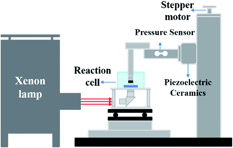 | ||
| Fig. 6 Schematic diagram of the photoelectric-effect-accelerated ECNL instrument. | ||
Characterization
An optical microscope (Olympus K-100, Olympus Co., Japan) was employed to observe the status of the template and the fabricated workpiece. A confocal laser microscopy setup (VK-X250, Keyence Co.) was employed to characterize the morphology and the profile of the imprinted 3D-MNSs in the semiconductors.Conclusions
We demonstrated photoelectric-effect-accelerated corrosion of GaAs induced by the contact potential between Pt and GaAs boundaries in an electrolyte environment. Under illumination of a xenon light source, electrons will be excited from the valence band to the conduction band and then move to the Pt side because of their different electronic work functions. Thus, the polarization of both the Pt/solution interface and the GaAs/solution interface is enhanced, and the interfacial charge transfer is accelerated kinetically. Kinetic investigations show that the rate-determining step is indeed the corrosion of GaAs. However, in practical ECNL processes, the mass balance of MnO4− anions and the removal of the products will cause a problem. The accelerated corrosion rate of GaAs will improve the ECNL efficiency. This unique electrochemical phenomenon makes ECNL more competitive as a microfabrication technique for functional 3D-MNSs directly on semiconductor wafers and has a prospective application in the semiconductor industry.Conflicts of interest
C. Guo and L. Zhang contributed equally. There are no conflicts to declare.Acknowledgements
The financial support from the National Natural Science Foundation of China (NSFC 21827802, 21573054 and 21621091) is appreciated.Notes and references
- D. W. Deberry, J. Electrochem. Soc., 1985, 132, 1022–1026 CrossRef CAS
.
- M. Pourbaix, Biomaterials, 1984, 5, 122–134 CrossRef CAS PubMed
- L. Liu, Y. Li and F. Wang, J. Mater. Sci. Technol., 2010, 26, 1–14 CrossRef CAS
- X. Liu, J. Xiong, Y. Lv and Y. Zuo, Prog. Org. Coat., 2009, 64, 497–503 CrossRef CAS
- T. N. Nguyen, J. B. Hubbard and G. B. McFadden, J. Coatings Technol., 1991, 63, 43–52 CAS
- D. Zhan, L. Han, J. Zhang, Q. He, Z.-W. Tian and Z.-Q. Tian, Chem. Soc. Rev., 2017, 46, 1526–1544 RSC
- D. Zhan, L. Han, J. Zhang, K. Shi, J.-Z. Zhou, Z.-W. Tian and Z.-Q. Tian, Acc. Chem. Res., 2016, 49, 2596–2604 CrossRef CAS PubMed
- S. Y. Chou, P. R. Krauss and P. J. Renstrom, Appl. Phys. Lett., 1995, 67, 3114–3116 CrossRef CAS
- L. J. Guo, Adv. Mater., 2007, 19, 495–513 CrossRef CAS
- S. Y. Chou, P. R. Krauss and P. J. Renstrom, Science, 1996, 272, 85–87 CrossRef CAS
- H. Schift, J. Vacuum Sci. Technol. B, 2008, 26, 458–480 CrossRef CAS
- C.-C. Yu and H.-L. Chen, Microelectron. Eng., 2015, 132, 98–119 CrossRef CAS
- J. K. Hwang, S. Cho, J. M. Dang, E. B. Kwak, K. Song, J. Moon and M. M. Sung, Nat. Nanotechnol., 2010, 5, 742–748 CrossRef CAS PubMed
- A. Cattoni, P. Ghenuche, A.-M. Haghiri-Gosnet, D. Decanini, J. Chen, J.-L. Pelouard and S. Collin, Nano Lett., 2011, 11, 3557–3563 CrossRef CAS PubMed
- R. Kawajiri, H. Takagishi, T. Masuda, T. Kaneda, K. Yamazaki, Y. Matsuki, T. Mitania and T. Shimoda, J. Mater. Chem. C, 2016, 4, 3385–3395 RSC
- T. Masuda, H. Takagishi, K. Yamazaki and T. Shimoda, ACS Appl. Mater. Interfaces, 2016, 8, 9969–9976 CrossRef CAS PubMed
- S. Y. Chou, K. Chris and G. Jian, Nature, 2002, 417, 835 CrossRef CAS PubMed
- Z. W. Tian, Z. D. Fen, Z. Q. Tian, X. D. Zhuo, J. Q. Mu, C. Z. Li, H. S. Lin, B. Ren, Z. X. Xie and W. L. Hu, Faraday Discuss., 1992, 94, 37–44 RSC
- L. Zhang, X.-Z. Ma, J.-L. Zhuang, C.-K. Qiu, C.-L. Du, J. Tang and Z.-W. Tian, Adv. Mater., 2007, 19, 3912–3918 CrossRef CAS
- X.-Z. Ma, L. Zhang, G.-H. Cao, Y. Lin and J. Tang, Electrochim. Acta, 2007, 52, 4191–4196 CrossRef CAS
- J. Zhang, L. Zhang, L. Han, Z.-W. Tian, Z.-Q. Tian and D. Zhan, Nanoscale, 2017, 9, 7476–7482 RSC
- J. Zhang, L. Zhang, W. Wang, L. Han, J.-C. Jia, Z.-W. Tian, Z.-Q. Tian and D. Zhan, Chem. Sci., 2017, 8, 2407–2412 RSC
- L. Zhang, J. Zhang, D. Yuan, L. Han, J.-Z. Zhou, Z.-W. Tian, Z.-Q. Tian and D. Zhan, Electrochem. Commun., 2017, 75, 1–4 CrossRef CAS
| This journal is © The Royal Society of Chemistry 2019 |