
 Open Access Article
 This Open Access Article is licensed under a Creative Commons Attribution-Non Commercial 3.0 Unported Licence
Multifunctional behavior of molecules comprising stacked cytosine–AgI–cytosine base pairs; towards conducting and photoluminescence silver-DNA nanowires†
Fátima
Linares
 *a,
Emilio
García-Fernández
b,
F. Javier
López-Garzón
c,
María
Domingo-García
c,
Angel
Orte
b,
Antonio
Rodríguez-Diéguez
c and
Miguel A.
Galindo
*c
*a,
Emilio
García-Fernández
b,
F. Javier
López-Garzón
c,
María
Domingo-García
c,
Angel
Orte
b,
Antonio
Rodríguez-Diéguez
c and
Miguel A.
Galindo
*c
aUnidad de Microscopía de Fuerza Atómica, Centro de Instrumentación Científica, Universidad de Granada, Paseo Prof. Juan Osorio s/n, 18003, Granada, Spain. E-mail: flinaor@ugr.es
bDepartamento de Fisicoquímica, Facultad de Farmacia, Universidad de Granada, Campus Cartuja, 18071, Granada, Spain
cDepartamento de Química Inorgánica, Facultad de Ciencias, Universidad de Granada, Avd. Fuentenueva s/n, 18071, Granada, Spain. E-mail: magalindo@ugr.es
First published on 8th November 2018
Abstract
DNA molecules containing a 1D silver array may be applied for nanotechnology applications, but first their conducting and photoluminescence behavior must be enhanced. Here we have synthesized and characterized three new helical compounds based on stacked silver–mediated cytosine base pairs [Ag(mC)2]X (mC = N1-methylcytosine; X = NO3 (1), BF4 (2) and ClO4 (3)), that contain uninterrupted polymeric AgI chains that run through the center of the helixes, comparable to related silver-DNA structures. The exposure of nanostructures of [Ag(mC)2]BF4 (2) to cold hydrogen plasma stimulates the reduction of the prearranged AgI polymeric chains to metallic silver along the material. This solvent-free reduction strategy leads to the compound [AgI(mC)2]X@Ag0 (2H) that contains uniformly well-distributed silver metallic nanostructures that are responsible for the new conducting and photoluminescence properties of the material. The presence of silver nanostructures alongside compound 2H has been evaluated by means of X-ray photoelectron spectroscopy (XPS), UV-vis spectroscopy, and X-ray powder diffraction (XRPD). The conducting and photoactive properties of 2H were studied by electrostatic force microscopy (EFM) and conducting-AFM (c-AFM), and photoluminescence microscopy (PL), respectively. The results demonstrate that the presence of well-organized metallic silver nanoentities on the material is responsible for the novel conductivity and photoactive properties of the material. This methodology can be employed for the generation of multifunctional silver-DNA related materials with tailored properties.
Introduction
Nanotechnology applications rely on the capability to prepare and control functional materials at the nanoscale with high precision.1–3 The development of novel methodologies that enhance this control has attracted the attention of scientists worldwide. In particular, the development of new strategies towards the fabrication of nanowires with tailored electronic and optical properties has been the subject of extensive efforts due to the practical applications they may offer for the miniaturization of electronic circuits. Importantly, in order to design new nanocircuits the correct organization of the nanowires must be precisely controlled. In this context, DNA has become an important tool for scientists, since intricate functional nanostructures can be prepared based on its sequence programmability, which offers potential applications in nanomachinery, sensing devices, drug delivery, and information processing.4–6 However, the concept of exploiting the self-organizing properties of DNA to create nanocircuits remains a great challenge and the source of much contentious discussion.7,8 This is due to the debatable conducting properties in natural DNA molecules, with some reports pointing towards the insulating behavior of long DNA molecules,9,10 whilst other studies have demonstrated charge transfer in short DNA molecules.11,12 The electronic properties of DNA molecules have been enhanced using various strategies, including the covalent attachment of functional groups13,14 or the deposition of a conducting material,15 including different metal atoms (i.e. Ag, Pd, Cu, Au, and Rh). Metallization of DNA molecules has proved to afford DNA-nanowires with improved conductivity,7,16–20 and has commonly been achieved through binding of metal ions to a DNA template followed by reduction of the ions positioned along the structure, typically using chemical, photochemical or electrochemical reduction.21 However, this strategy cannot guarantee the complete control over the deposition process, and various regions can be metalized to different extents, hampering the ability of metal–DNA-based systems to conduct electricity. A new way to precisely control the stoichiometry and the position of the metal ions have been proven using DNA molecules containing the so-called metal-mediated base pairs. In these cases, the metal ions are placed inside the double helix structure, by programming its sequence, with hydrogen bonding that holds the two stands together being replaced by coordination bonds between the bases. Following this strategy continuous 1D linear chains of AgI ions can be generated inside the DNA duplex,22 thus demonstrating that new metallo-DNA nanowires could be rationally prepared. Studies of the conducting properties of these types of systems remain ongoing and no clear conclusions regarding the enhancement of their conductivity have been drawn yet. DNA molecules containing C–AgI–C silver-mediated base pairs (C = cystosine) have been well studied,22–24 and in the last decade several conducting studies have been performed on such metallized DNA molecules. The results indicate that the increase or decrease of charge transfer may depend on the DNA sequence employed.25,26 A recent study shows that the intercalation of AgI ions between the mismatched cytosine bases leads to more efficient charge transfer.27 However, a potential method to increase the conductivity of these systems would be to reduce of the confined AgI ions to Ag0. It is well known that the reduction of controlled amounts of silver ions introduced on DNA strands leads to the formation and stabilization of silver nanoclusters (AgNCs) which have photoluminescence properties due to their small size (<2 nm).28,29 In these instances, the reduction of AgI–DNA complexes is carried out in solution,30–32 and consequently the native structure of the resulting AgNC–DNA systems can be significantly altered.33 If high-precision nanocircuit architectures based on DNA molecules containing silver-mediated base pairs, with conductive and/or photoemissive properties, are to be developed, a methodology that leads to the formation of metallic silver whilst preserving the structure of the material will be needed. In this regard, methodologies based on photoreduction processes can promote the reduction of the silver ions to metallic silver along DNA molecules;34 however the presence of solvents with additional chemical functionalities (i.e. salts35 and hydroxyl groups36) has been proven to play an important role in the reduction process. Our attempts to use a solvent- and additive-free photoreduction methodology, exclusively using UV irradiation over 1 to 12 h (254 nm), were unsuccessful to form well-distributed silver metallic throughout the herein studied 1D nanostructures. A new approach to be explored is the use of controlled cold hydrogen plasma to promote the reduction of silver ions to afford metallic silver whilst maintaining the integrity of previously organized Ag-material nanostructures in the solid state. In principle, this strategy could be used to reduce silver ions organized in DNA molecules comprising silver-mediated base pairs once they have been correctly organized and immobilized on a surface support. Moreover, such an approach will avoid the use of any additional solvents and/or chemicals, which can disrupt the organization of the structures. Finally, this proposed strategy could enable the formation of uniformly distributed nanoscale metallic silver entities along the solid material, which ultimately may improve the conducting and/or photoemissive properties of the material.With the aim of proving this hypothesis, in this work we explore the use of cold hydrogen plasma to reduce silver ions confined in helixes consisting of contiguous C–AgI–C base pairs, in order to promote the formation of well-organized metallic silver, which may subsequently enhance the conducting and photoactive properties of the nanomaterial. We have chosen these helical complexes as an initial approach towards the study of more complex DNA double helix structures since the stabilizing effect of cytosine towards the formation of AgNC is well known. The molecular structure of the herein described silver complexes, studied by X-ray diffraction, confirmed the formation of double helixes containing an uninterrupted 1D silver chain that runs through the central axis. These complexes can be formed on a solid surface support and their morphology and conducting properties were studied by atomic force microcopy (AFM), electric force microscopy (EFM) and conducting AFM (c-AFM). We demonstrate by means of X-ray photoelectron spectroscopy (XPS), solid UV-vis spectroscopy, X-ray powder diffraction (XRPD) and photoluminescence (PL) microscopy that the silver ions can be reduced by exposure to cold hydrogen plasma, leading to the formation of silver nanostructures that are uniformly distributed along the structures. Finally, we prove that the presence of these metallic silver nanospecies can enhance both the conductivity and photoluminescence behavior of the material, as indicated by EFM and c-AFM analysis, and PL microscopy, respectively.
Results and discussion
Synthesis and characterization of the complexes
The formation of helixes 1, 2 and 3 was carried out by reaction of methylcytosine (mC) with the corresponding AgI salt; nitrate, tetrafluoroborate or perchlorate, respectively. In all cases, single crystals of complexes [Ag(mC)2]X (X = NO3, BF4, ClO4), suitable for X-ray diffraction analysis, were obtained within the next 48 h upon slow evaporation of the reaction solution. In all cases, the analysis of the molecular structure, by means of X-ray diffraction, revealed the formation of helixes consisting of stacked mC–AgI–mC homobase pairs. The silver-mediated base pairs are lined up on top of each other giving rise to the formation of argentophilic interactions that run through the centre of the helix. Inter-cytosine-pair hydrogen bonds are also observed which further support the formation of the helical structures. These assemblies resemble the structure recently reported by Terrón et al. for the formation of a double helix generated by contiguous hC–AgI–hC base pairs (hC = hexylcytosine).37 An important difference of the herein reported structures is the obtaining of individual chiral crystals for 2 and 3, although the overall samples were racemic mixtures. In addition, the three polymeric silver chains show shorter argentophilic contacts, probably due to the presence of less steric effects induced by the methyl group compared to the hexyl alkyl chains.Compound 1 crystallizes in the monoclinic space group P21/c. The asymmetric unit consists of ten [Ag(mC)2]+ units, ten nitrate anions and ten crystallization water molecules (Fig. 1a). The AgI ions are two-coordinated and adopt a linear geometry. The mC units act as monodentate ligands and coordinate to the silver ions via their N1 atom [Ag–N1 2.102(15) to 2.250(20) Å] forming silver-mediated base pairs, mC–AgI–mC. The base pairs are organized on top of each other leading to the formation of argentophilic interactions [Ag–Ag 2.902(2) to 3.088(2) Å], which are significantly shorter than those found in an analogous silver double helix [3.162 to 3.235 Å]37 and in a DNA molecule with an 1D array of silver ions [3.2 to 3.4 Å].22 The mC units are in a cisoid orientation showing propeller twist angles from 48.79 to 66.32°. This Watson–Crick pairing arrangement is different to the anti-Watson–Crick (transoid) orientation described inside a DNA duplex38 and in a particular silver complex where two AgI ions coordinate via N–Ag–O connectivity in mC ligands.39 In addition, DFT calculations indicate that the transoid orientation in C–AgI–C pairs may be favoured.40 However, the occurrence of the cisoid arrangement is not exceptional, and it has been also described in the structure reported by Terron et al.37 as well as inside DNA22 and RNA23 molecules.
 | ||
| Fig. 1 (a) Scheme for the [Ag(mC)2]+ silver-mediated base pair. (b) Different perspectives of the polymeric [Ag(mC)2]NO3 in the asymmetric unit of 1 and (c) in the asymmetric unit of [Ag(mC)2]BF4 (2). Counter ions and crystallization water molecules have been omitted for clarity. (d) View of 2 from the crystallographic b axis (Ag, yellow sphere; mC ligand, grey; BF4, blue). | ||
In complex 1, as well as in 2 and 3 (vide infra), the cisoid arrangement is preferred, which is stabilized by the formation of contiguous π–π interactions [distance between the centroids pertaining to mC rings from 3.477 to 4.199 Å] as well as hydrogen bonds between the keto and amino groups of diagonal opposite mC ligands of the two complementary strands [hydrogen bonds in the range of 2.843 to 3.022 Å].
All these interactions give rise to the formation of a double helix structure consisting of consecutive mC–AgI–mC base pairs that include an uninterrupted 1D silver array running through the helical axis. Interestingly, the silver array is not completely linear all along the asymmetric unit and different <Ag–Ag–Ag angles [137.69° to 179.22°] can be observed (Fig. 1b). A complete turn of the helix contains an average of ten base pairs within the asymmetric unit. The helix diameter is c.a. 11 Å.
In the case of compounds 2 and 3, the selected crystals are similar right-handed helix compounds, and therefore only the data for 2 are described here. Complex 2 crystallizes in the monoclinic space group P212121. The asymmetric unit consists of eight [Ag(mC)2]+ units and eight crystallization tetrafluoroborate anions (Fig. 1c). In the same way as 1, the AgI ions coordinate to two mC units via their N1 atom [Ag–N1 range 2.149(12)–2.206(10) Å] adopting a linear geometry and generating chains formed by silver-mediated base pairs mC–AgI–mC. The argentophilic interactions [Ag–Ag 2.9025(16) to 2.9786(16)Å] are also shorter than those previously found for an analogous system,37 and related silver-DNA molecule.22 The mC units are in a cisoid orientation showing propeller twist angles [32.53° to 68.74°]. This arrangement facilitates the formation of contiguous π–π interactions [distance between the centroids from 3.550 to 3.929 Å] that are interrupted every six silver-mediated base pairs. The presence of hydrogen bonds is also observed between the keto and amino groups of diagonal opposite mC ligands of the two complementary strands. All these interactions support the formation of a double helix structure analogous to 1. In this case the linearity of the silver array is slightly more disrupted than that in compound 1 (<Ag–Ag–Ag angles from [125.44° to 169.85°]) (Fig. 1c). The helix turn is now completed every nine base pairs and consequently comprises two asymmetric units. The helix diameter is also c.a. 11 Å.
Surface studies of complexes [Ag(mC)2]X [X = NO3 (1), BF4, (2) ClO4 (3)]
Atomic force microscopy (AFM) was employed to study the morphology of the silver chains of complexes 1, 2 and 3 immobilized on solid substrate surfaces. The synthesis of the complexes was carried out both on mica and silicon substrates by drop-casting of a solution containing mC and AgI ions (details in the Experimental section) and waiting until all solvent evaporates. Initial efforts to form 1, 2 or 3 on surfaces showed that the complex organization depends on both the surface composition and the complex counter ion. The use of the mica substrate did not always enable the formation of 1D structures, although the best results were obtained for compound 1 after several attempts (Fig. 2). | ||
| Fig. 2 Z-height images of 1 crystals on a mica substrate: red line profile corresponding to the red graph and green line corresponding to the green graph on the right showing a height of 1.2–1.4 nm. Blue line profile corresponding to a height of c.a. 1 nm. | ||
The silicon substrate seems to facilitate the formation of larger 1D structures, and are more reproducible, and the best results were obtained for compound 2 (Fig. 3 and S2, ESI†). Therefore, silico wafers were chosen for the preparation of the 1D nanostructures on the surface. The analysis of the AFM images of 1 showed the formation of 1D structures organized in a grid pattern and the presence of single helixes of the complex. Line profile studies revealed a structural height value of c.a. 1.2 nm that agrees with the diameter value (1.1–1.2 nm) measured in the crystal structure of the double helixes (vide supra). The majority of the structures are organized perpendicular to each other giving rise to the formation of a grid pattern, with lengths in the range of 750 to 1000 nm.
 | ||
| Fig. 3 Left: AFM Z-height images of microcrystals 2 prepared on a Si/SiO2 substrate. Right: line profile for height. | ||
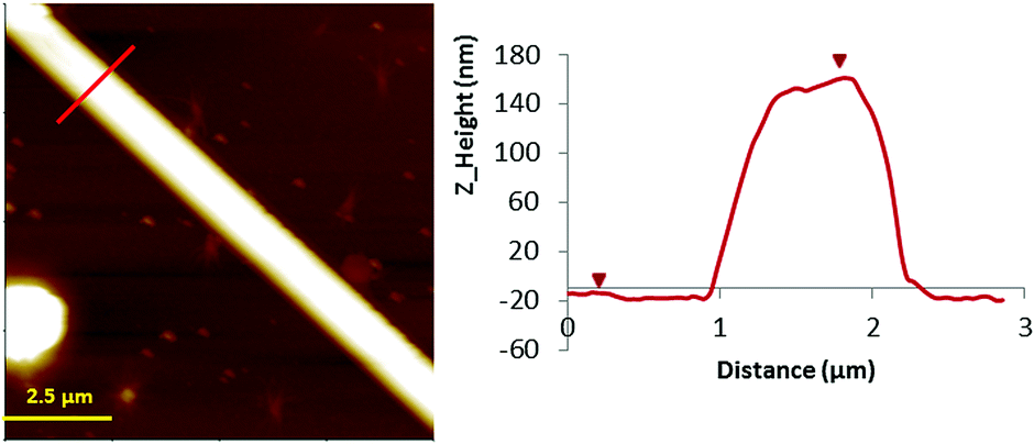
In contrast, when the samples were prepared on Si/SiO2 substrates, larger structures were observed using the same concentration of the sample prepared on mica. In this case, the nanostructures prepared on the Si/SiO2 substrate obtained for complex 2 are shown in Fig. 3 (and Fig. S2, ESI†). AFM images show the microstructures of 2 with a height of 160 nm, thus indicating the formation of nanostructures. Fourier transform infrared spectroscopy (FTIR) was used to demonstrate the chemical equivalence of the compound prepared on the surface with the crystalline solid material studied by X-ray diffraction (Fig. S1, ESI†).
Reduction of AgI ions to metallic silver; preparation and characterization of the complex [AgI(mC)]BF4@Ag0 (2H)
As previously described, complex 2 formed the smallest needle-like nanostructures when prepared on Si/SiO2 substrates. Consequently, 2 was employed to evaluate the conducting properties of the silver-chain structures using the EFM and c-AFM techniques.The reduction of the prearranged AgI-chains can lead to the formation of well-distributed silver metallic nanostructures, which can enhance the conducting and photoemission properties of the material. For this task, cold hydrogen plasma was employed as a reducing agent to form metallic silver. To assess the changes in these properties following the reduction of the AgI ions, conductivity and photoemission studies were performed on the structures before and after the reduction process.
We have explored this solvent-free methodology in an effort to avoid the use of additional chemicals and to preserve the original structure of the material whilst producing distinctive metallic silver entities along the surface of the material.
Microcrystals of 2 were exposed to hydrogen plasma, giving rise to the compound [AgI(mC)]BF4@Ag0 (2H), containing the formation of well-arranged metallic silver along the structure. The presence of Ag0 entities in complex 2H was then studied by X-ray photoelectron spectroscopy (XPS), X-ray powder diffraction, UV-vis spectroscopy and transmission electron microscopy (TEM). The XPS survey scan spectrum registered for 2 and 2H (Fig. S3, ESI†) exhibits peaks for C1s, N1s and O1s arising from the mC ligand, as well as B1s, F1s and Ag3d due to the presence of silver tetrafluoroborate.
In the case of 2, the high-resolution spectrum of the Ag3d region (Fig. 4) shows two distinct peaks with binding energy at 367.1 and 373.1 eV corresponding to AgI 3d3/2 and 3d5/2 due to spin–orbit coupling. However, after the reduction treatment, the spectrum for 2H shows the Ag3d peaks shifted to lower energy. Moreover, the curve-fitting requires two new components to accurately reproduce the shape of the experimental spectrum, confirming the existence of two different silver species. The two new components appear at 366.8 and 372.8 eV. The splitting between them of 6 eV is in agreement with the values in the literature for Ag0. Indeed the two components are due to the Ag0 3d spin–orbit coupling. From the XPS data the degree of reduction has been estimated to be 32.7% and 44.4%, for 5 min and 10 min of reduction treatment, respectively. The high resolution XPS spectra of the valence band region are shown in the ESI.† This region of the spectrum is very useful to distinguish subtle differences in the electronic properties of solids.41,42 These spectra show that after hydrogen plasma reduction there is a large electron photoemission at binding energy values very close to zero.
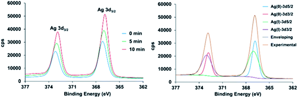 | ||
| Fig. 4 Left: High resolution XPS spectrum of the Ag3d region for compound 2 before and after exposure to cold hydrogen plasma. Right: The experimental data (orange line) was fitted (dash line) to the sum of the 3d5/2 and 3d3/2 contributions of Ag0 (blue and red lines, respectively) and AgI (green and purple lines, respectively). The inset legend gives the time period of exposure to the hydrogen plasma. | ||
This means that the electron density near the Fermi level has been increased, suggesting the presence of metallic silver and therefore conducting behavior (Fig. S4, ESI†).
X-ray powder diffraction (XRPD) shows that the basic features of the diffraction pattern for 2 and 2H are maintained (Fig. 5), which is indicative of the preservation of the main characteristics of the crystal structure after exposure to hydrogen plasma. Nonetheless, in the case of 2H a new sharp and strong peak is observed at a 2θ value of 38°, which can be assigned to the (111) reflection of metallic Ag. This is consistent with the reduction of the AgI ions at the crystal surface of the material with the concomitant formation of small metallic silver nanostructures with a 111 preferential orientation. No other additional reflections of metallic silver can be appreciated, which suggests the formation of small metallic particles that are beyond the detection limits of the XRD instrumentation (3 nm).
 | ||
| Fig. 5 XRD diffraction pattern for complexes 2 and 2H, before and after exposure to cold hydrogen plasma, respectively. The inset legends indicate the time period of exposure to the hydrogen plasma. | ||
Photoluminescence emission of complexes 2 and 2H
Solid-state UV-vis spectroscopy carried out upon complexes 2 and 2H also confirmed the formation of metallic silver (Fig. S5, ESI†). The spectrum of 2 exhibits an absorption band around 260 nm where the mC ligand absorbs. In the case of 2H a new broad absorption band arises between 350 and 500 nm, with a maximum absorption at 435 nm that can be associated with the surface plasmon resonance (SPR) of metallic silver generated by the reduction treatment.These results further confirm that metallic silver nanostructures have been formed as a consequence of the reduction treatment with cold hydrogen plasma. Consequently, the presence of potential silver nanostructures in 2 and 2H was studied by means of PL microscopy and PL lifetime imaging microscopy (PL-FLIM). PL-FLIM microscopy has the advantage of collecting spatial maps of both the luminescence emission intensity and the temporal evolution of the excited state, via the PL emission decay and the PL lifetime, τ. AgNCs have been reported to exhibit spectrally tunable PL emission, depending on the fabrication method and the templating agent.43 Hence, the PL emissive properties are also indicative of the formation of AgNCs within the crystals, and a promising and interesting feature of these materials. Since AgNCs usually exhibit dual-band PL emission,44 we collected PL-FLIM images of crystals of 2H in two different detection channels, as detailed in the methods section, one for the green PL (centered at 520 nm) and another for the red emission (centered at 685 nm). This represents a multi-parametric imaging technique, in which both spectral and kinetic information is accessible.
The 2H crystals showed PL emission upon excitation at 375 nm all over the crystal surface, indicating the formation of AgNCs over the material (Fig. 6A).
 | ||
| Fig. 6 (a) PL emission in the 520 nm and the 685 nm channels of microcrystals of compounds 2 and 2H upon excitation at 375 nm. (b) I520/I685 ratio imaging of the same fragments on a pseudocolor scale spanning from one order of magnitude excess of green emission to one order of magnitude excess of red emission. (c) PL-FLIM imaging in the 520 nm and the 685 nm channels of a 2H microcrystal. (d) PL lifetime distributions of 2H microcrystals in the 520 nm (gray histogram) and the 685 nm (red histogram) channels. The histograms are average values from three different 2H fragments. In all the images, scale-bars represent 10 μm. | ||
In clear contrast with these results, crystals of 2 did only show negligible PL emission that may be mainly attributed to the fluorescence emission from the mC bases as it was mainly detected in the green channel (Fig. 6A). Interestingly, the dual channel approach allowed us to map the crystal PL emission using a ratiometric composition of the green emission (I520) over the red emission (I685). The I520/I685 ratiometric imaging revealed the presence of hot spots, usually distributed in a straight-line fashion along 2H crystals (Fig. 6B and S6A, ESI†). PL-FLIM microscopy also allowed us to focus our attention on the PL lifetime, τ, reporting on the kinetics of the excitons. The PL decay traces on 2H crystals exhibited a short-lived contribution of 0.4 ns, and a second long lifetime component. The short-lived component may be related to emission from mC bases, known to display fast kinetics.45Fig. 6C (and Fig. S6B and S6C, ESI†) shows representative PL-FLIM images of 2H crystals in the green (520 nm) and the red (685 nm) channels. Interestingly, differences in the emission PL lifetimes were found in the green and the red spectral regions. In the green channel, the PL lifetime values were centered around 3.3 ns (Fig. 6D), in good agreement with the reported lifetime values between 2.9 and 3.9 ns of green-emitting AgNCs templated in C-rich single-stranded DNA with a G-rich self-loop.38 In contrast, the PL lifetime distribution in the red channel was centred around 2.4 ns, also in perfect agreement with previous values reported for red-emitting, C-rich-single-strand-templated AgNCs.46 These results confirm the presence of AgNCs emitting in different spectral regions, and therefore, comprising different numbers of atoms, overlapped over the crystal structure. By analyzing the statistical weight of the long PL lifetime, compared to the short emission lifetime, it was striking that the regions that displayed more red emission also exhibited a higher weight of the long PL lifetime (Fig. S7, ESI†). This fact also entails that the red emission is directly related to PL of the plasmonically excited AgNCs, without potential artifacts coming from elastic or inelastic scattering of light.
Electrical studies of complexes 2 and 2H
Electrical characterization was performed using both a variant form of electrostatic force microscopy (often referred to as Scanning Conductance Microscopy, SCM)47 and conducting AFM (c-AFM).Complex 2 was prepared on Si/SiO2 (200 nm) substrate surfaces, and subsequently complex 2H was generated by exposure of the sample to hydrogen plasma, as previously described. Initially, EFM phase imaging (where a phase shift indicates the electrical nature of the 1D material; e.g. a negative phase shift implies the structures to be electrically conducting) was carried out since this technique quickly provides qualitative information about the electrical properties of different materials deposited on a substrate.48 It has been previously demonstrated that in SCM the electrically conductive material displays negative shifts as the tip passes over the structures, whilst the insulating material exhibits a positive phase shift.49
AFM studies registered for complex 2, prepared on silicon wafers, show the formation of 1D structures with a height of c.a. 160 nm (vide supra). The corresponding phase images acquired at different direct currents (−6 to +6 V) did not display any significant negative phase shift of the structure (Fig. S8, ESI†). By comparison, AFM analysis of 2H revealed smaller structures with a height of c.a. 30 nm, indicating that there has been a loss of part of the crystal during exposure to the cold hydrogen plasma (Fig. 7b). Notably, in this case, the corresponding EFM phase images (Fig. 7d–i) acquired at different applied voltages (−5 to +5 V) show a dark contrast over the full range of bias potentials applied, indicating the existence of charge conduction in 2H. The magnitude of these phase shifts depends on the geometry of the sample, the height of the tip above the surface and (dc) bias (V).17,47
 | ||
| Fig. 7 (a) Parabolic dependence of the phase shift vs. bias voltages for 2H between −10 and 10 V; (b) Z-height image of the chain aligned on a Si/SiO2 surface; (c) profile of the topography image. (d, e, g and h) EFM phase images at a lift height of 40 nm and tip/sample bias of (d) +2.5 V, (e) −2.5 V, (g) +5.5 V and (h) −5.5 V. (f) A line section through the phase image of the chain visible in this image at +2.5 V. (i) A line section through the phase image of the chain visible in this image at +5.5 V. The cantilever spring constant (k) = 129.9 N m−1 and the quality factor (Q) = 274. | ||
The profile of the phase shift across the structure of 2H (Fig. 7f and i) resemble a W-shape, as previously perceived for other semiconducting materials.17,20 The width of the phase images is enlarged compared to height AFM images because of the diffuse long-range nature of the tip-sample interactions. A representation of the phase shift versus the applied bias displays a parabolic relationship across voltages between −10 and +10 V (Fig. 7a). Subsequently, c-AFM measurements were performed on 2 and 2H in order to further study and compare the conducting properties of these materials and provide a quantitative assessment of the conductivity observed in 2H. For this purpose we prepared complex 2 on silicon chips and exposed them to cold hydrogen plasma to obtain the reduced 2H material. A drop of Ga–In eutectic was placed at the end of the corresponding microcrystal to provide an electrical contact. The metallic AFM tip was then used to act as the second electrical contact to the sample. During our initial c-AFM experiments we found that the high forces exerted upon the samples by the tip result in individual chains being broken during the raster scanning of the tip across the sample (results not shown). In order to avoid this problem, larger structures of 2 and 2H were employed for c-AFM studies, compared to those employed for EFM measurements, since they were less prone to damage during scanning, though still required careful regulation of the applied force by the tip using PinPointTM (Park Systems) c-AFM Mode. Moreover the exposure time to hydrogen plasma was also reduced to 7 minutes as longer exposure times appeared to weaken the structures for these sets of experiments.
The initial c-AFM experiments performed on 2 demonstrated the absence of perceptible conducting properties, in agreement with the results obtained by EFM. The area of the sample surface scanned during measurements was located c.a. 50 μm away from the eutectic contact on a 100 μm long crystal (Fig. S9, ESI†). In this regard, while we have not observed conductivity for 2, it is worth noting that previous studies performed on polycytosine sequences of 11 mer C–AgI–C base pairs, by means of scanning tunneling microscopy break-junction, revealed higher single molecule conductance with respect to the canonical G–C oligonucleotide, although the technique and the sample are different to that reported here.27
In contrast, when the measurements were performed for 2H the results showed a notable increase in conductance, which agrees with the EFM results. Fig. 8 illustrates the topography of a structure of 2H and its electrical properties when a voltage of ±10 V is applied to the sample, demonstrating the presence of a current signal throughout 2H. The average heights of the structures were c.a. 400 nm indicating that they consist of multiple silver-chains bundled together into thicker assemblies.
 | ||
Fig. 8 PinPoint c-AFM height image of the 2H chain. (a) Z-height image (height 400 nm); (b) current signal at +10 V. (c) Dual Line profile from the Z-height image (red line) and current map (green line), highlighting that the current associated with this structure is of the order of nanoamps. (d) F–d curve for PinPoint c-AFM mode. Selected parameters: control height: 1.8 μm; stiffness threshold: 1.20 nN; approach time: 4.0 ms; retract time: 2.0 ms; (e) 3D overlay for Z-height and current signals (X![[thin space (1/6-em)]](https://www.rsc.org/images/entities/char_2009.gif) :Y:Z = 1:1:1.5). :Y:Z = 1:1:1.5). | ||
In this case, the area of the sample surface scanned during measurements was located at 85 μm away from the eutectic contact on the crystal chosen for the measurements (Fig. S10, ESI†). A current map simultaneously acquired alongside the height data is shown in Fig. 8b, at an applied bias of +10 V and on the order of up to 1 nA. The zero current observed when the tip was placed above a clean area of the Si/SiO2 substrate proves that the measured current is a consequence of the electrical properties of 2H.
Fig. 8b also shows the existence of different conducting regions, which may be explained by poor mechanical contact between the tip and an uneven surface with depressions (Fig. 8e).
The maximum specific conductivity registered for this structure was 1.25 nA and demonstrated that the use of cold hydrogen plasma can promote the formation of metallic silver nanostructures in 2H that ultimately enhance the conducting properties of the material. It is worth mentioning that in essence, the size of the material, the amount of metal coating and the distance to the Ga–In eutectic electrode influence the conducting properties of the sample. In this regard, DNA-based silver molecules, which can resemble the herein reported structures, have shown different conductivity depending of the conditions of the experiments.
However, in these previous studies different amounts of silver ions were initially deposited along DNA templates and then reduced to form metallic silver using diverse procedures (e.g. chemical reduction or electrochemical process). In general, the resulting structures displayed metallic silver granular aggregates along the DNA molecules and significant conductivity (50 to 400 nA)16,50,51 compared to the herein reported material, when a bias/potential was applied. Recently, narrow and smooth DNA-silver nanowires were obtained by transferring silver atoms from silver nanoparticles (AgNPs) to DNA molecules, although no conducting data were reported.52 However, following a similar procedure using gold nanoparticles (AuNPs), small (less than 13 nm height), narrow and uniform DNA-gold structures were obtained which showed a long range conductivity of c.a. 1 nA.7
Importantly, the herein reported strategy does not alter the initial composition of the material, does not require the use of additional chemicals to promote the reduction of the AgI ions, and is able to enhance the conductivity and photoemission behavior of the pre-organized material. The reduction of AgI within the material may generate thin films of silver nanostructures along the material that are in sufficient intimate contact (via metal/metal contact interactions) to allow charge migration through the material. Therefore, this methodology can be employed to enhance the conducting properties of various solid materials containing well organized AgI in the solid state without the addition of other chemicals.
Conclusions
Three different helical silver complexes 1, 2 and 3 have been prepared and characterized by single crystal X-ray diffraction. The molecular structure revealed the formation of helixes consisting of stacked mC–AgI–mC homobase pairs, with the presence of contiguous AgI chains running through the centre of the helixes and with the presence of argentophilic interactions, that resemble DNA molecules containing a 1D array of silver ions.22 The complexes were also prepared on solid support surfaces and their morphology, conductivity and photoluminescence behavior were studied by means of AFM, EFM, c-AFM, and PL microscopy, respectively. In an effort to enhance the conducting and photoemissive properties of these materials, complex 2 was exposed to cold hydrogen plasma, leading to the formation of compound 2H possessing metallic silver nanostructures along the material. The presence of metallic silver was confirmed by XPS, UV-vis spectroscopy, XPRD and PL-FLIM. XPRD also confirmed that the reduction process did not alter the crystal structure of the complex. Compound 2H showed PL emission along the structure that reveals the formation of plasmonic emissive silver nanoclusters. In consequence, the presence of these metallic silver nanoentities significantly improved the photoemissive properties of the material. Moreover, the conducting properties of 2H were evaluated by EFM and c-AFM, confirming the new conducting behavior of the material, which can be also attributed to the presence of metallic silver entities. Although more studies will be required to comprehensively evaluate how electrical charges travel through this material, it is reasonable to propose that the observed conductivity is dominated by a conduction bridge through the well-ordered metallic entities. Importantly, these results offer a new strategy to prepare and modify the conducting and photoluminescence properties of a solid material that contains prearranged silver ion chains, e.g. DNA molecules containing sequential silver-mediated base pairs, even at the nanoscale.Experimental
Materials
Reagents were purchased from Aldrich and used as received. N1-methylcytosine was synthesized according to literature methods.53 Elemental analysis was performed on a Thermo Scientific Flash 2000, and UV-vis spectra were recorded on an Agilent Technologies Cary 100 Spectrophotometer. XPS spectra were recorded on a Kratos Axis Ultra DLD spectrometer. Monochromatic AlKα radiation in constant analyser energy mode with a pass energy of 160 and 20 eV (for the survey and high resolution spectra, respectively) was used. The C 1s transition at 285 eV was used as the reference value. After background correction, the high-resolution spectra were fitted to Lorentzian and Gaussian curves using XPS CASA software. In all cases, a standard Shirley baseline was used to separate the real signal from the background.54 A JASCO 6200 FTIR Spectrophotometer with SPECTRA MANAGER v2 software was used to obtain infrared spectra in the mid-infrared area (4000–400 cm−1) with a resolution of 0.25 cm−1.General procedure for the synthesis of [Ag(N1-methylcytosine)2]X (X = NO3 (1), BF4 (2), ClO4 (3))
A general procedure will proceed as follows; to a water solution of N1-methylcytosine (mC) (150 mg, 1.2 mmol) was added a water solution of the corresponding silver salt (0.6 mmol). The solution was stirred for 30 min in the dark and then filtered off through a syringe filter (0.45 μm cellulose acetate membrane) to remove any insoluble impurities. The clear solution was left to crystallize and after a few days crystals suitable for X-ray diffraction were collected. In the case of complex 1, a non-crystalline phase was also obtained as a white powder.[Ag(N1-methylcytosine)2]NO3 (1): Yield 21%. Elemental Analysis corresponding to [C10H14N7O5Ag·(H2O)1.4]: calcd C 26.96, N 22.01, H 3.80; found, C 26.63, N 22.23, H 3.79. [Ag(N1-methylcytosine)2]BF4 (2): Yield 35%. Elemental Analysis corresponding to [C10H14N6O2BF4Ag·(H2O)0.5]: calcd C 26.45, N 18.51, H 3.33; found, C 26.49, N 18.13, H 3.66. [Ag(N1-methylcytosine)2]ClO4 (3): Yield 33%. Elemental Analysis corresponding to [C10H14N6O6ClAg·(H2O)0.5]: calcd C 25.74, N 18.01, H 3.24; found, C 25.89, N 18.14, H 3.52.
Single-crystal X-ray structure determination
X-ray data collection of suitable single crystals of compounds 1–3 was done at 100(2) K on a Bruker VENTURE area detector equipped with graphite monochromated Mo-Kα radiation (λ = 0.71073 Å) by applying the ω-scan method. The data reduction was performed with APEX2 software55 and corrected for absorption using SADABS.56 Crystal structures were solved by direct methods using the SIR97 program57 and refined by full-matrix least-squares on F2 including all reflections using anisotropic displacement parameters by means of the Olex2 v1.2 crystallographic package58 and the SHELXL-2014 program.59,60 All hydrogen atoms were included as fixed contributions riding on attached atoms with isotropic thermal displacement parameters 1.2 times or 1.5 times those of their parent atoms for the organic ligands. In general, the overall quality of the crystals was low and this results in a low diffraction for the three compounds. Several crystals of 1, 2 and 3 were measured and the structure was solved from the best data we were able to collect. Attempts to solve disorder problems with two nitrate and ten crystallization water molecules with two tetrafluoroborate anions and with one perchlorate anion failed in compounds 1, 2 and 3, respectively. We have used the BYPASS procedure61 implemented in Olex2 v1.2 to eliminate these molecules. Final R(F), wR(F2) and goodness of fit agreement factors, details on the data collection and analysis can be found in Table S1 (ESI).†Details of the bond distances of compounds are summarized in Table S2 (ESI).† Crystallographic data (excluding structure factors) for the structures reported in this paper have been deposited with the Cambridge Crystallographic Data Center as supplementary publication no. CCDC 1847831–1847833.
Preparation of substrates for AFM, EFM and c-AFM studies
For AFM analysis of topography, freshly cleaved Muscovite Mica V1 Quality was used. Electrical characterization by EFM and c-AFM was carried out on Si/SiO2 substrates; the SiO2 layer ∼200 nm thickness. N-doped Si 〈111〉 wafers were used for both modes. The wafers were cut into small pieces (1.0 × 1.0 cm) with a diamond tip pen, and then sequentially cleaned using a cotton bud soaked in acetone, propanol and finally water. Further treatment was carried out on Si 〈111〉 wafers with ‘piranha’ solution (4:1 H2SO4/H2O2) for 45 min for electrostatic force microscopy measurements. The wafer was rinsed thoroughly with milliQ water, providing a highly hydrophilic surface rich in OH-termini. The SiO2 layer was removed from one side of the wafer by applying a single drop of HF solution (48% in H2O) onto the wafer surface. The HF solution was left on the wafer for about 30 s, removed from the substrate surface and rinsed with copious amounts of milliQ water.
Surface immobilization of complexes for atomic force microscope (AFM) studies
A freshly cleaved mica surface (Muscovite Mica V1 Quality, Aname) was employed without further treatment. The synthesis of complex 1 was carried out on mica by deposition of a solution containing mC and AgNO3. The procedure consisted in mixing 7 μL of an aqueous reaction solution (10 mg mC, 6.7 mg AgNO3, 3 mL milliQ water, and 1 mL NH3) and 7 μL of milliQ water. The mixture was left to evaporate on the mica surface. The sample was covered and stored in the dark for 15 h at room temperature without any disturbance to allow for the nanostructure formation to proceed. This procedure was repeated several times until appropriate organization of 1 could be observed by AFM. It is worth mentioning that the same procedure did not work to prepare complexes 2 or 3 at the nanoscale on a mica surface, as much larger assemblies and aggregates were formed. The preparation of complexes 2 and 3 at the nanoscale was substantially more successful when a silicon substrate was employed, and therefore this will be the preferred method for the study of the conducting properties by EFM and c-AFM measurements.Surface immobilization of complexes for EFM and c-AFM studies
The preparation of the complexes was done on Si/SiO2 chips with an oxide thickness of ∼200 nm. The synthesis of the complexes followed the same procedure as that described above for mica. In this case, the best 1D nanostructures were obtained for complex 2. Therefore, the EFM and c-AFM studies were performed for silver-chains obtained from 2 and 2H (upon reduction using hydrogen plasma). The in situ synthesis was carried out correspondingly as previously described on a mica surface.Cold hydrogen plasma reduction of AgI ions
The treatment to reduce AgI ions to metallic silver was achieved by exposing microcrystals of 2 formed on Si/SiO2 chips to cold hydrogen plasma for 10 min. The reaction was carried out in a commercial device (Europlasma Junior Advanced SS). The equipment produces plasma by using a 2.45 GHz microwave source. The samples, once in the device chamber, were outgassed to a residual pressure of 50 mTorr before the treatments. Prior to the treatment, hydrogen was flowed for 5 minutes (15 cm3 min−1) up to a stable pressure of 280–300 mTorr. The source power was set to 700 W.Photoluminescence lifetime imaging microscopy (PL-FLIM)
A small amount of the studied crystals from compound 2 or reduced 2H was homogenously deposited over a coverslip (Menzel-Gläser, ∅25 mm #1) and covered with microscopy immersion oil (Cargille laboratories) to decrease light scattering. Small fragments of the crystal, deposited on the glass surface, were subsequently located with the transmitted light of the microscope. PL-FLIM images were recorded with a MicroTime 200 system (PicoQuant GmbH, Germany) based on single photon timing with the time-tagged time-resolved (TTTR) methodology, which permits the reconstruction of the fluorescence decay traces from the microcrystals in the confocal volume. A 375 nm pulsed diode laser (LDH series from PicoQuant) controlled with a Sepia II driver (PicoQuant) was employed as an excitation source at a 20 MHz repetition rate. The corresponding excitation laser beam was directed into the specimen through an apochromatic oil immersion objective (100 × 1.4 NA) of an inverted microscope system (IX-71, Olympus, Japan). The PL light was collected back and filtered by the main dichroic (DCXR 375 nm, AHF-Chroma) and a cutoff filter (LP 405 nm, AHF Semrock), and spatially filtered through a 75 μm pinhole. The emitted photons were separated by a dichroic (DCXR 600 nm, AHF-Chroma) and directed to two avalanche photodiode detectors (SPCM-AQR-14, Perkin Elmer) after passing through a 520 nm/35 (AHF-Semrock) or a 685 nm/70 (Omega Filters) band pass filter, respectively. Photon counting and time tagging were performed within a Time-Harp 200 module (PicoQuant), with a time resolution of 29 ps per channel. For imaging a region, the sample was raster-scanned with an x-y piezo-driven device (Physik Instrumente, Germany). The image data, with a 512 × 512 pixel resolution, were normally acquired over a surface area of 20 × 20 μm and a collection time of 0.60 ms per pixel.The PL-FLIM images were analysed using SymphoTime 32 software (PicoQuant). To obtain the fitted FLIM images, a reconstructed instrument response function was employed to analyse the PL decay histogram of each pixel within the whole image using an exponential model. The decay histograms were fitted by applying the maximum likelihood estimator (MLE), which yields correct parameter sets for low count rates. A previous spatial binning of 5 × 5 pixels and prehistogramming of 8 temporal channels (for a final resolution of 232 ps per channel) were used to achieve a larger number of counts in each pixel. For the samples of compound 2 the decay model was a monoexponential function in which the decay time was a freely adjustable parameter. However, the presence of an intense short component for the reduced 2H crystals required a biexponential model in which one of the decay times was fixed at 0.4 ns, whereas the other decay time was a freely adjustable parameter. To highlight the distribution of times, amplitude intensity images of each decay time were reported in combination with a lifetime image.
I 520/I685 ratio images were obtained by dividing the intensity images collected in each channel, and the ratio represented by a pseudo-color scale, with the image intensity modulated by the total I520 + I685 intensity, via a home-coded script in MathCad 15.0 (PTC).
Scanning probe microscopy (AFM, EFM and c-AFM)
AFM imaging was performed in non-contact mode in air, using an NX20 Park Systems instrument (Park Systems Corp.), with ACTA cantilevers (silicon cantilevers, resonant frequency 200–400 kHz, spring force constant 25–75 N m−1, Park Systems). Data acquisition was carried out using SmartScan software version 1.0 and XEI Data Processing and Analysis software version 4.3.0 Build2 (Park Systems Corp). The NX20 equipment is supported by an Active Vibration Isolation System (AVIS) model AVI-200S/LP (Table Stable Ltd).A variant method of EFM has been used as a contactless means of qualitatively assessing the electrical properties of 2 structures prior to quantitative measurement of conductivity. The method is based on the storage of energy in the tip/chain/substrate capacitor and the chain conductance influences the measurement via the RC time constant for polarization of the nanocrystals. A detailed description of the operation of this method has been reported elsewhere.17,62 The phase shift between the driving force and the tip motion is recorded as a function of applied dc bias (V) as the tip crosses above the chain at a constant lift height (typically a value set within the range of 40–100 nm). EFM measurements were performed using a two-pass method, in which the first pass of the tip over a scan line gathers topographical data in standard non-contact mode, and the second pass of the tip records the EFM phase information. During the second pass, the tip travelled over the sample surface at a constant lift height (set at 40 nm), whilst an independently controlled dc bias was applied to the sample (from ±1.5 to ±10 V), with the tip grounded. The cantilevers used for these measurements were NCSTAu which are designed for non-contact or soft tapping mode imaging. A metallic layer (Au) is coated on both sides of the cantilever. The typical tip radius of curvature is less than 50 nm. These probes are 140–160 μm long, with a resonant frequency of about 129.9 kHz, a quality factor Q = 274, and a spring constant between 1.2 and 29 N m−1.
Conductive AFM (c-AFM) was performed at room temperature with the gentle PinPoint i-AFM mode which was the key to acquiring reproducible and reliable topography and c-AFM images on the 2 chains. The conventional contact and conductive AFM have pros and cons, but this mode allows the best of both spatial resolution and current sensitivity, whilst minimizing the lateral forces with optimized current measurement over different sample surfaces. The measurement procedure can be explained in three steps: (1) the XY scanner stops during acquisition; (2) the tip approaches the surface, measures the current and retracts from the surface over a few ms (4 ms) to achieve an interaction force preset (1.2 nN); (3) record the approach height and maintain the Z distance. The force was held constant while the current is measured, and then the tip is retracted and moved to the next pixel. This method differs significantly from conventional c-AFM because the tip retracts and approaches each pixel rather than adjusting the tip height to maintain a constant oscillation amplitude. This scan mode does require more time (approximately 30 min for a 256 × 256 pixel image) but results in highly reproducible images. In contrast to conventional c-AFM, this technique eliminates friction, which reduces tip-sample deterioration. For conductive measurements (c-AFM), CDTCONTR probes were used (the CDT diamond coating is highly doped and the total resistance measured in contact to a platinum surface is <10 kOhm). These probes are 440–460 μm long, with a resonant frequency of about 20 kHz and a spring constant between 0.1 and 1.7 N m−1. Electrical contact was made by applying a drop of In/Ga eutectic to one corner of the chip and to the metallic chuck. The current is measured directly after the tip using a preamplifier with a gain of 1011 V/A (ULCA). c-AFM imaging was performed with an applied bias of +10 V. The imaged area was about 1 mm away from the In/Ga contact.
Conflicts of interest
There are no conflicts to declare.Acknowledgements
Financial support from the Spanish MINECO (CTQ2017-89311-P), Junta de Andalucía (FQM-2293) and Universidad de Granada (Reincorporación Plan Propio) are acknowledged. This study was partially supported by the “Unidad de Excelencia de Química aplicada a Biomedicina y Medioambiente”, Universidad de Granada. We thank Dr Scott M. D. Watson for discussions and guidance during the preparation of the manuscript, and Dr Ismael Drubi for technical support.Notes and references
- M. R. Jones, N. C. Seeman and C. A. Mirkin, Science, 2015, 347, 1260901 CrossRef PubMed.
- P. W. K. Rothemund, Nature, 2006, 440, 297–302 CrossRef CAS PubMed.
- N. C. Seeman, Nature, 2003, 421, 427–431 CrossRef PubMed.
- O. I. Wilner and I. Willner, Chem. Rev., 2012, 112, 2528–2556 CrossRef CAS PubMed.
- Z.-G. Wang, C. Song and B. Ding, Small, 2013, 9, 2210–2222 CrossRef CAS PubMed.
- H. Pei, X. Zuo, D. Zhu, Q. Huang and C. Fan, Acc. Chem. Res., 2014, 550, 550–559 CrossRef PubMed.
- A. Stern, G. Eidelshtein, R. Zhuravel, G. I. Livshits, D. Rotem, A. Kotlyar and D. Porath, Adv. Mater., 2018, 1800433 CrossRef PubMed.
- S. M. D. Watson, A. R. Pike, J. Pate, A. Houlton and B. R. Horrocks, Nanoscale, 2014, 6, 4027–4037 RSC.
- A. J. Storm, J. Van Noort, S. De Vries and C. Dekker, Appl. Phys. Lett., 2001, 79, 3881–3883 CrossRef CAS.
- P. J. De Pablo, F. Moreno-Herrero, J. Colchero, J. Gómez Herrero, P. Herrero, A. M. Baró, P. Ordejón, J. M. Soler and E. Artacho, Phys. Rev. Lett., 2000, 85, 4992–4995 CrossRef CAS PubMed.
- J. D. Slinker, N. B. Muren, S. E. Renfrew and J. K. Barton, Nat. Chem., 2011, 3, 228–233 CrossRef CAS PubMed.
- M. Bixon, B. Giese, S. Wessely, T. Langenbacher, M. E. Michel-Beyerle and J. Jortner, Proc. Natl. Acad. Sci. U. S. A., 1999, 96, 11713–11716 CrossRef CAS.
- W. Chen and G. B. Schuster, J. Am. Chem. Soc., 2013, 135, 4438–4449 CrossRef CAS PubMed.
- T. Nguyen, A. Brewer and E. Stulz, Angew. Chem., Int. Ed., 2009, 48, 1974–1977 CrossRef CAS PubMed.
- K. Ijiro and H. Mitomo, Polym. J., 2017, 49, 815–824 CrossRef CAS.
- E. Braun, Y. Eichen, U. Sivan and G. Ben-Yoseph, Nature, 1998, 391, 775–778 CrossRef CAS PubMed.
- R. Hassanien, S. A. F. Al-Said, L. Šiller, R. Little, N. G. Wright, A. Houlton and B. R. Horrocks, Nanotechnology, 2012, 23, 075601 CrossRef PubMed.
- H. D. A. Mohamed, S. M. D. Watson, B. R. Horrocks and A. Houlton, J. Mater. Chem. C, 2015, 3, 438–446 RSC.
- A. Houlton, A. R. Pike, M. A. Galindo and B. R. Horrocks, Chem. Commun., 2009, 1797–1806 RSC.
- J. Pate, F. Zamora, S. M. D. Watson, N. G. Wright, B. R. Horrocks and A. Houlton, J. Mater. Chem. C, 2014, 2, 9265–9273 RSC.
- Z. Chen, C. Liu, F. Cao, J. Ren and X. Qu, Chem. Soc. Rev., 2018, 47, 4017–4072 RSC.
- J. Kondo, Y. Tada, T. Dairaku, Y. Hattori, H. Saneyoshi, A. Ono and Y. Tanaka, Nat. Chem., 2017, 9, 956–960 CrossRef CAS PubMed.
- J. Kondo, Y. Tada, T. Dairaku, H. Saneyoshi, I. Okamoto, Y. Tanaka and A. Ono, Angew. Chem., Int. Ed., 2015, 54, 13323–13326 CrossRef CAS PubMed.
- A. Ono, S. Cao, H. Togashi, M. Tashiro, T. Fujimoto, T. Machinami, S. Oda, Y. Miyake, I. Okamoto and Y. Tanaka, Chem. Commun., 2008, 4825–4827 RSC.
- H. Gong and X. Li, Analyst, 2011, 136, 2242–2246 RSC.
- Z. Lin, X. Li and H. B. Kraatz, Anal. Chem., 2011, 83, 6896–6901 CrossRef CAS PubMed.
- E. Toomey, J. Xu, S. Vecchioni, L. Rothschild, S. Wind and G. E. Fernandes, J. Phys. Chem. C, 2016, 120, 7804–7809 CrossRef CAS.
- S. Y. New, S. T. Lee and X. D. Su, Nanoscale, 2016, 8, 17729–17746 RSC.
- E. Gwinn, D. Schultz, S. M. Copp, S. Swasey and S. Ralph, Nanomaterials, 2015, 5, 180–207 CrossRef PubMed.
- J. T. Petty, J. Zheng, N. V. Hud and R. M. Dickson, J. Am. Chem. Soc., 2004, 126, 5207–5212 CrossRef CAS PubMed.
- J. M. Obliosca, C. Liu and H.-C. Yeh, Nanoscale, 2013, 5, 8443–8461 RSC.
- I. Díez and R. H. A. Ras, Nanoscale, 2011, 3, 1963–1970 RSC.
- J. T. Petty, O. O. Sergev, M. Ganguly, I. J. Rankine, D. M. Chevrier and P. Zhang, J. Am. Chem. Soc., 2016, 138, 3469–3477 CrossRef CAS PubMed.
- L. Berti, A. Alessandrini and P. Facci, J. Am. Chem. Soc., 2005, 127, 11216–11217 CrossRef CAS PubMed.
- A. A. Zinchenko, N. Chen and S. Murata, Chem. Lett., 2008, 37, 1096–1097 CrossRef CAS.
- D. Majumdar, A. Singha, P. K. Mondal and S. Kundu, ACS Appl. Mater. Interfaces, 2013, 5, 7798–7807 CrossRef CAS PubMed.
- A. Terrón, B. Moreno-Vachiano, A. Bauzá, A. García-Raso, J. J. Fiol, M. Barceló-Oliver, E. Molins and A. F. Frontera, Chem.–Eur. J., 2017, 23, 2103–2108 CrossRef PubMed.
- H. Liu, F. Shen, P. Haruehanroengra, Q. Yao, Y. Cheng, Y. Chen, C. Yang, J. Zhang, B. Wu, Q. Luo, R. Cui, J. Li, J. Ma, J. Sheng and J. Gan, Angew. Chem., Int. Ed., 2017, 56, 9430–9434 CrossRef CAS PubMed.
- T. Kistenmacher, M. Rossi and L. Marzilli, Inorg. Chem., 1979, 18, 240–244 CrossRef CAS.
- L. A. Espinosa Leal, A. Karpenko, S. Swasey, E. G. Gwinn, V. Rojas-Cervellera, C. Rovira and O. Lopez-Acevedo, J. Phys. Chem. Lett., 2015, 6, 4061–4066 CrossRef CAS PubMed.
- J. Matthew, Surf. Interface Anal., 2004, 36, 1647 CrossRef CAS.
- V. K. Abdelkader-Fernández, F. Morales-Lara, M. Melguizo, C. García-Gallarín, R. López-Garzón, M. L. Godino-Salido, F. J. López-Garzón, M. Domingo-García and M. J. Pérez-Mendoza, Appl. Surf. Sci., 2015, 357, 1410–1418 CrossRef.
- Y. Lu and W. Chen, Chem. Soc. Rev., 2012, 41, 3594–3623 RSC.
- C. Bu, L. Mu, X. Cao, M. Chen, G. She and W. Shi, Nanotechnology, 2018, 417, 257–269 Search PubMed.
- R. J. Malone, A. M. Miller and B. Kohler, Photochem. Photobiol., 2003, 77, 158–164 CrossRef CAS PubMed.
- C. Li and C. Wei, Sens. Actuators, B, 2017, 240, 451–458 CrossRef CAS.
- M. Al-Hinai, R. Hassanien, S. M. D. Watson, N. G. Wright, A. Houlton and B. R. Horrocks, Nanotechnology, 2016, 27, 095704 CrossRef PubMed.
- C. Staii, A. T. Johnson and N. J. Pinto, Nano Lett., 2004, 4, 859–862 CrossRef CAS.
- M. Bockrath, N. Markovic, A. Shepard, M. Tinkham, L. Gurevich, L. P. Kouwenhoven, M. W. Wu and L. L. Sohn, Nano Lett., 2002, 2, 187–190 CrossRef CAS.
- S. A. Farha Al-Said, R. Hassanien, J. Hannant, M. A. Galindo, S. Pruneanu, A. R. Pike, A. Houlton and B. R. Horrocks, Electrochem. Commun., 2009, 11, 550–553 CrossRef CAS.
- G. Ban, R. Dong, K. Li, H. Han and X. Yan, Nanoscale Res. Lett., 2009, 4, 321–326 CrossRef CAS PubMed.
- G. Eidelshtein, N. Fardian-Melamed, V. Gutkin, D. Basmanov, D. Klinov, D. Rotem, Y. Levi-Kalisman, D. Porath and A. Kotlyar, Adv. Mater., 2016, 28, 4839–4844 CrossRef CAS PubMed.
- E. Greco, A. E. Aliev, V. G. H. Lafitte, K. Bala, D. Duncan, L. Pilon, P. Golding and H. C. Hailes, New J. Chem., 2010, 34, 2634–2642 RSC.
- V. K. Abdelkader, M. Domingo-García, M. Melguizo, R. López-Garzón, F. Javier López-Garzón and M. Pérez-Mendoza, Carbon, 2015, 93, 276–285 CrossRef CAS.
- Bruker, APEX3 Software, Bruker AXS Inc., Madison, Wisconsin, USA, vol. 1, 2016 Search PubMed.
- G. M. Sheldrick, Program for Empirical Adsorption Correction, Inst. Inorg. Chem. Univ. Gottingen, Ger., 1996 Search PubMed.
- A. Altomare, M. C. Burla, M. Camalli, G. L. Cascarano, C. Giacovazzo, A. Guagliardi, A. Grazia, G. Moliterni, G. Polidori and R. Spagna, J. Appl. Crystallogr., 1999, 32, 115–119 CrossRef CAS.
- L. J. Farrugia, J. Appl. Crystallogr., 2012, 45, 849–854 CrossRef CAS.
- G. M. Sheldrick, Program for Crystal Structure Refinement, Univ. Gottingen, Ger., 2014 Search PubMed.
- G. M. Sheldrick, Acta Crystallogr., Sect. A: Found. Crystallogr., 2008, 64, 112–122 CrossRef CAS PubMed.
- A. L. Spek and IUCr, Acta Crystallogr., Sect. C: Struct. Chem., 2015, 71, 9–18 CrossRef CAS PubMed.
- A. Houlton and S. M. D. Watson, Annu. Rep. Prog. Chem., Sect. A: Inorg. Chem., 2011, 107, 21–42 RSC.
Footnote |
| † Electronic supplementary information (ESI) available: Extended information on this article is available for bond distances (Å) (molecular structures of 1–3); XPS survey spectra, FITR spectroscopy; valence band XPS and UV-vis spectra for 2 and 2H; additional photoemission images; EFM measurement, phase shift vs. bias voltages and EFM and c-AFM measurements for 2, before reduction with cold hydrogen plasma; optical microscope image showing crystals of 2H employed during c-AFM studies. CCDC 1847831–1847833. For ESI and crystallographic data in CIF or other electronic format see DOI: 10.1039/c8sc04036b |
| This journal is © The Royal Society of Chemistry 2019 |