 Open Access Article
Step-by-step monitoring of CVD-graphene during wet transfer by Raman spectroscopy†
Zehao Wua,
Xuewei Zhanga,
Atanu Das a,
Jinglan Liua,
Zhenxing Zoua,
Zilong Zhanga,
Yang Xiab,
Pei Zhao
 *a and
Hongtao Wang*a
aCenter for X-Mechanics and Institute of Applied Mechanics, Zhejiang University, Hangzhou 310012, P. R. China. E-mail: peizhao@zju.edu.cn; htw@zju.edu.cn
bInstitute of Microelectronics, Chinese Academy of Sciences, Beijing 100029, China
First published on 16th December 2019
Abstract
Transfer acts as a crucial bridge between the chemical vapor deposition (CVD) synthesis of large-scale graphene and its applications, but the quality evolution of a graphene film during transfer remains unclear. Here we use scanning Raman spectroscopy to monitor as-grown graphene during each step of wet transfer including floating on etchant solution, loaded onto a target substrate, and with additional annealing. Results show that the etchant solution results in strong compressive strain and p-type doping to floating graphene, but both are significantly reduced after the sample is loaded and rinsed especially for the doping. An annealing treatment increases the compressive strain in graphene but hardly its doping level. Moreover, when a poly(methyl methacrylate) (PMMA) layer is used to assist the transfer, it does not only increase the p-type doping of floating graphene but also lowers the crystalline quality of annealed graphene. Therefore, to obtain graphene with better quality, besides the attempts of improving CVD synthesis for its larger domain sizes, universal and easy-to-use polymer-free transfer techniques must be developed as well.
Introduction
As a one-atom-thick material, graphene has become one of the main focuses of materials research owing to its extraordinary physical, chemical and electronic properties.1 Among different synthetic techniques for graphene,2–6 the chemical vapor deposition (CVD) approach of hydrocarbons on Cu substrates6–8 has demonstrated the best graphene yield with the highest uniformity, largest film size and comparable quality with that derived by mechanical microcleavage.1,9 However, a disadvantage of the CVD method is that after growth, a transfer process of graphene from Cu to the substrates of interests is required before the practical applications such as field-effect transistors (FETs).10 A most popular transfer method is the ‘wet transfer’ that uses a polymer film covering graphene—such as poly(methyl methacrylate) (PMMA)—as a protection layer and removes the underneath Cu substrate within an etchant solution, followed by picking up the isolated polymer/graphene layer onto other surfaces and dissolving the polymer with a proper solvent.6 However, due to the introduction of the polymer layer onto the graphene surface, the quality of as-grown graphene is significantly reduced by various additional effects, for instance, the polymer residues always lead to a reduction of graphene's electronic performance, the strain and stress in graphene during transfer generate new wrinkles and other defects, and so on.11–13 However, so far most of the previous reports have focused on the quality of transferred graphene after the polymer is removed,14–18 and few of them have studied the influence of other factors such as the etchant solution19 or the polymer layer. A systematic investigation on how each step during the wet transfer affects the quality of as-grown graphene is of high importance for the further improvement of the transfer techniques and the resultant graphene quality. Therefore, it is desirable to characterize the quality evolution of graphene step-by-step during the wet transfer.On the other hand, Raman spectroscopy is a powerful and nondestructive tool for the rapid analysis of graphene.20–22 The Raman spectrum of a graphene sample exhibits three featured peaks known as D, G, and 2D peaks which are very sensitive to external stimuli such as defects,23–26 doping,27,28 strain,29–31 magnetic fields,32,33 temperature,34 etc. Therefore, collecting Raman signals and contour maps from graphene can behave as a fast and efficient approach to monitor its quality during and after the wet transfer process.
In this study, we use scanning Raman spectroscopy to monitor as-grown graphene during each step of wet transfer including floating on etchant solution, loaded onto a target substrate, and with additional annealing. Results show that the etchant solution results in strong compressive strain and p-type doping to floating graphene, but both are significantly reduced after the sample is loaded and rinsed especially for the doping. An annealing treatment increases the compressive strain in graphene but hardly its doping level. Moreover, when a PMMA layer is used to assist the transfer, it does not only increase the p-type doping of floating graphene but also lowers the crystalline quality of annealed graphene. Therefore, to obtain graphene with better quality, transfer of graphene without polymer protection needs to be considered.
Results and discussion
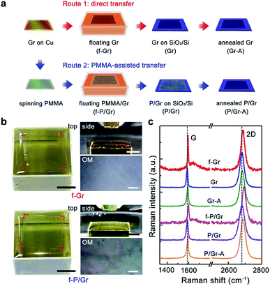
The schematic of direct (polymer-free, red arrows) and PMMA-assisted (blue arrows) transfer routes for graphene onto SiO2/Si substrates is shown in Fig. 1a. The direct transfer includes three key steps of floating graphene (f-Gr), graphene loaded on a SiO2/Si substrate (Gr) and annealed graphene on a SiO2/Si substrate (Gr-A). For PMMA-assisted transfer, it starts with the spin-coating of a PMMA layer onto graphene, followed by floating PMMA/graphene (f-P/Gr), graphene loaded on a SiO2/Si substrate after PMMA removal (P/Gr, the most widely studied case by researchers), and annealed graphene on a SiO2/Si transferred in the previous step (P/Gr-A). Our focus in this work is the samples during/after the six steps of f-Gr, Gr, Gr-A, f-P/Gr, P/Gr and P/Gr-A. It needs to be mentioned that as-grown graphene on Cu is not studied here mainly due to that the strong fluorescence from Cu makes it difficult to obtain the accurate spectrum from graphene, as shown in Fig. S1, ESI.† However, considering that all the samples used in this work are synthesized using the same CVD recipe with the same initial quality, as well as that the first crucial step in wet transfer of graphene is to remove the Cu substrate by an etchant solution, it is reasonable that we start our analysis by comparing the floating graphene samples. The up and down panels in Fig. 1b show the experimental setups of f-Gr and f-P/Gr, respectively, including photographs of the floating samples on FeCl3 solution from the top and side views, and their optical microscopy (OM) images. The graphene size adopted in our experiments is approximately 2 cm by 2 cm, similar to that in most lab tests. Compared with f-Gr that without a PMMA layer, f-P/Gr exhibits more apparent edges in the top view photograph and an optical birefringence from the PMMA layer. Typical Raman spectra measured from f-Gr, Gr, Gr-A, f-P/Gr, P/Gr and P/Gr-A are presented in Fig. 1c. It needs to be mentioned that for f-Gr, n-heptane is adopted to assist stabilizing the graphene film. The Raman spectrum of n-heptane derived directly from its liquid is shown in Fig. S2, ESI,† whose peaks are mainly distributed within 1300 to 1450 cm−1 and not overlap the peaks for graphene, and more importantly, during the experiments a much lower amount of n-heptane is used and its peaks are all negligible when compared with those from graphene.For all these spectra, only G (∼1590 cm−1) and 2D (∼2680 cm−1) peaks are observed without apparent D (∼1350 cm−1) peaks, indicating the high quality of these samples through our experiments.22 Notably, for f-P/Gr even with a PMMA layer (∼200–300 nm thick) covering on top, clear Raman signals can still be collected within the range of interest (1300–2800 cm−1). Moreover, in both f-Gr and f-P/Gr a relatively weak and broad fluorescence peak located at ∼1650 cm−1 is observed. Therefore, all the obtained G and 2D peaks are carefully fitted by Lorentzians after the spectrum decomposition.
More importantly, the centers of the G and 2D peaks in Fig. 1c are not at the same position as we draw reference lines across the G and 2D peak centers of the P/Gr spectrum especially for the two floating samples of f-Gr and f-P/Gr. These peak shifts are usually originated from the modifications of graphene lattices and/or the electronic structure. For instance, a compressive/tensile strain results in a blueshift/redshift for both the G and 2D peaks,30,31 a p-type doping results in a blueshift for both peaks, and an n-type doping leads to a redshift for the 2D peak but blueshift for the G peak.28 Such effects to graphene in each transfer step will be discussed in more details below.
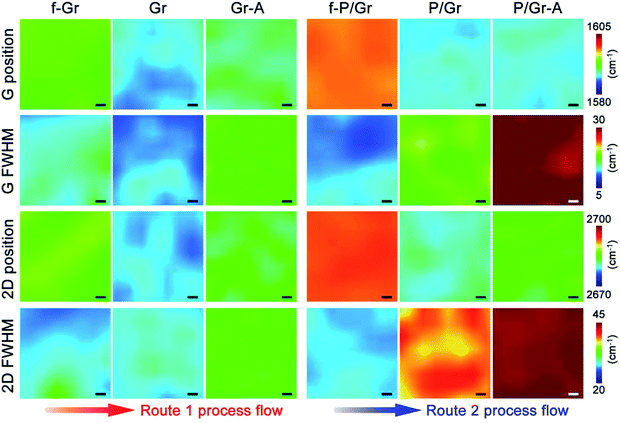
Fig. 2 presents the Raman maps for f-Gr, Gr, Gr-A, f-P/Gr, P/Gr and P/Gr-A, including their G peak center positions, G peak full-width-at-half-maximum (FWHM), 2D peak center positions and 2D peak FWHM. These maps are listed in two panels, with the direct transfer on the left and PMMA-assisted transfer on the right. In each panel, the process flow of transfer steps is listed from left to right, so that the evolution of graphene's Raman peaks during the transfer is shown in this way as well. During the direct transfer, when graphene is picked up from solution onto a substrate, both its G and 2D peaks redshift by ∼7 cm−1, whereas their widths maintain almost the same. With additional annealing, its G peak blueshifts by ∼5 cm−1 and 2D peak blueshifts by ∼4 cm−1, and both peak widths are broadened by ∼2 cm−1. On the other hand, during PMMA-assisted transfer, compared with floating graphene without PMMA, both the G and 2D peaks of floating graphene with PMMA significantly blueshift by ∼7 cm−1, but their peak widths are slightly narrower by ∼2 cm−1. After the sample is picked up and the removal of PMMA, its G peak redshifts by ∼10 cm−1 and 2D peak by ∼12 cm−1, to the positions almost the same as those of graphene by the direct transfer. However, the widths of these peaks are broadened by 5 cm−1 and 13 cm−1 for the G and 2D peaks, respectively, much broader than those from graphene by direct transfer. A more considerable change occurs when this sample is further annealed. Although the G peak maintains its position and the 2D peak slightly blueshifts by 3 cm−1, the widths of both peaks are significantly increased by 10 cm−1 and 12 cm−1, respectively.
These results imply that compared with graphene by direct transfer, when PMMA is used graphene experiences a higher level of external strain from the environment and/or doping from the contact agents.28,30,31 In Fig. 3 we collect the data of graphene from above maps and summarize them using scatter plots of the peak width against the peak center position for the G and 2D peaks. Here we discuss these peak widths first. Apparently, graphene samples floating on the etchant solution (f-Gr and f-P/Gr) exhibit the smallest peak widths. Considering the width of a generated peak is usually inversely proportional to phonon lifetime and proportional to phonon scattering rate,35,36 the narrow peaks from f-Gr and f-P/Gr are indicative of their high crystalline structure with fewer scattering sites for phonons. These scattering sites are usually defects and impurities in graphene that are different from the sp2-carbon honeycomb-like crystalline structures.37,38 After they are picked up onto substrates, with or without PMMA their G and 2D peak widths are both broadened. We attribute such broadening to the increased phonon scattering by the existence of a supporting substrate. Moreover, the peak widths of graphene transferred with PMMA are broadened by a larger extent, suggesting that the removal of PMMA lowers the structural quality of graphene by leaving residues or creating defects in graphene as new scattering sites,14 but they are too few to be detected by the Raman D peaks. After annealing, for direct transferred graphene both its G and 2D peak widths maintain the same, indicating that the sample quality is not affected by such treatment. However, for graphene transferred with PMMA, its both peaks are broadened after the annealing, especially for the G peak. As demonstrated in previous reports, the main propose of annealing is to remove polymer residues attached on the graphene surface.14,39 Cheng et al. demonstrated that the removal of PMMA can result in sp3-type point defects formed by polymer residues with carbon atoms in graphene.40 Therefore, it is safe to conclude that such residue removal by annealing actually results in more scattering of phonons in graphene, probably due to the loss of carbon atoms together with polymer residues.
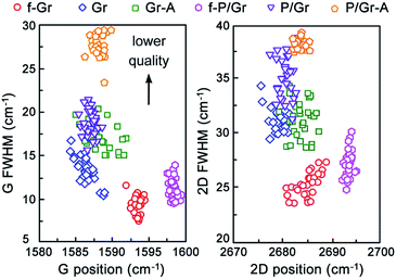 | ||
| Fig. 3 Scatter plots of peak width against peak center position for the G and 2D peaks of graphene at different steps during direct and PMMA-assisted transfer. | ||
Now we turn to the discussion of peak shifting during the transfer of graphene. As we mentioned previously, both strain and doping can result in shift of Raman peaks.27–31 In Fig. 4 we plot a correlation map of the G and 2D peak positions for graphene at each step of direct and PMMA-assisted transfer. Two solid lines indicative of zero doping (left) and zero strain (right) are shown across the map as well, with the arrow directions pointing to the increase of ‘pure’ compressive strain and p-type doping, respectively. In other words, graphene with Raman peak positions located on these lines can be considered as being affected only by strain or doping. These two lines are derived based on the data from ref. 18 and 29, respectively, and the cross point of these lines indicates the neutral state of graphene. Previous studies have demonstrated that CVD graphene are subject to nonuniform compressive strains resulted from the mismatch of graphene and Cu lattices.41,42 For both floating graphene, they are under a combined state of compressive strain and p-type doping, and f-P/Gr exhibits much higher strain and doping levels than f-Gr, resulted from the strong constraint effect and charge transfer to graphene by PMMA, respectively.18 After picked up onto a SiO2/Si substrate, through each route the doping in graphene can be largely reduced to almost zero, but the compressive strain is maintained although it is significantly reduced. The compression state of graphene by PMMA-assisted transfer is consistent with the previous reports. With further annealing, the compressive strain in both Gr and P/Gr increases, but no apparent doping from the SiO2/Si substrates is observed, much smaller than the previous results by Kong et al., in which a doping effect from the underlying SiO2/Si can be transferred to graphene.18,28
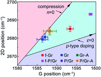 | ||
| Fig. 4 A correlation map of the G and 2D peak positions of graphene at different steps in direct and PMMA-assisted transfer. | ||
Finally, we discuss more on the annealing treatment to transferred graphene. Annealing is usually considered as an efficient way to improve the electrical performance of transferred graphene by further removing the polymer residues and enhance the contact between graphene and the substrate.28 However, our above results clearly demonstrate that annealing will result in the lowering of graphene's crystalline quality, probably due to the loss of carbon atoms together with polymer residues. To test the electrical performance of annealed graphene, we measured the sheet resistance of transferred graphene before and after annealing, for samples by direct and PMMA-assisted transfer. The results are presented in Fig. 5. Without PMMA, the sheet resistance of transferred graphene is ∼590–860 Ω □−1, which is reduced to ∼370–650 Ω □−1 after annealing. On the other hand, with PMMA involved, the sheet resistance of transferred graphene is ∼900–1050 Ω □−1, and is reduced to ∼720–810 Ω □−1 by annealing. Apparently, although with the probability of lowering the crystalline quality of graphene, annealing still behaves as a promising way to improve the graphene electrical conductivity. However, the negative effects in both the crystallinity and the electrical performance from the PMMA protection layer must be eliminated, and universal and easy-to-use polymer-free transfer techniques must be developed in the future of graphene research.
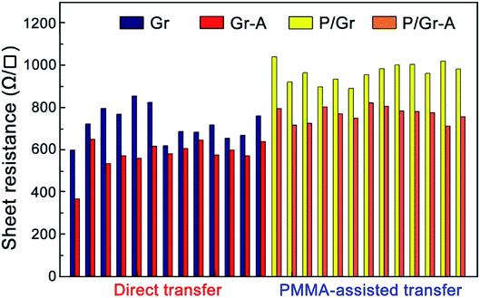 | ||
| Fig. 5 Sheet resistance of graphene samples before and after the annealing treatments transferred by polymer-free or PMMA-assisted methods. | ||
Experimental
Graphene synthesis
Polycrystalline graphene was synthesized on commercially available Cu (Suzhou Fukuda Metal Co. Ltd) foils using a low-pressure CVD process.6 In details, a Cu foil was loaded into the CVD quartz chamber and heated to 1060 °C within a H2 atmosphere for 70 min, to remove the metal surface impurities and increase the metal grain size. A self-limiting growth of monolayer graphene was then conducted using 10 sccm H2 and 1 sccm CH4 for 30 min.Graphene transfer
For direct (polymer-free) transfer of graphene, a 1 M FeCl3 aqueous solution was slightly overloaded in a container to form a convex liquid surface, on which the CVD-grown graphene/Cu foil was carefully floated. The graphene surface was then covered by several drops of n-heptane as a liquid protection layer. After the Cu foil was etched, isolated graphene was directly printed and picked up using a SiO2 (300 nm)/Si substrate and rinsed by deionized water.For PMMA-assisted transfer, a thin layer of PMMA (4 wt% in anisole, AR-P 679.04, Allresist GmbH, Germany) was spin-coated onto as-grown graphene on a Cu foil at a speed of 3000 rpm and baked at 105 °C. The same amount of FeCl3 as the direct transfer was used, and after the total removal of the Cu foil, the isolated graphene/PMMA film was rinsed and loaded onto a SiO2/Si substrate, and the PMMA layer was then removed by dichloromethane at 45 °C.
The annealing treatment of transferred graphene was conducted by placing the samples in a clean CVD quartz tube at 360 °C with 100 sccm H2 for 6 hours.
Raman measurements and other characterizations
The Raman spectra and maps were collected using confocal micro-Raman spectroscopy (LabRAM HR Evolution, Horiba Co. Ltd.) with a laser excitation wavelength of 532 nm and a power of 12.5 mW. A long-focal length 50× objective lens with NA = 0.95 and standard grating (1800 grad per mm) were used, and the laser spot size was estimated to be 1.4 μm. The Raman spectra had a resolution of <0.5 cm−1 and the spatial resolution in all the Raman maps was as 5 μm. All the measured spectral data were analyzed using the LabSpe6 software.For graphene sheet resistance measurements, standard four-point probe technique at room temperature was used. The interval distances between the linearly arranged probes were 1 mm, and each sample was measured for more than ten times.
Conclusions
In summary, we have used scanning Raman spectroscopy as an efficient tool to resolve the quality evolution of as-grown graphene during wet transfer, by monitoring the shift of the center position and width of Raman G and 2D peaks collected from graphene at each step during transfer: floating on etchant solution, loaded onto a target substrate, and with additional annealing. Results show that the etchant solution results in strong compressive strain and p-type doping to floating graphene, but both are significantly reduced after the sample is picked up and rinsed especially for the doping. Annealing increases the compression level in graphene but hardly increases its doping level. Moreover, when a PMMA layer is used to assist the transfer, it does not only increase the p-type doping of floating graphene but also lowers the crystalline quality of annealed graphene as indicated by the largely broadened Raman peak width. Therefore, to obtain graphene with better quality, besides the attempts of improving CVD synthesis for its larger domain sizes, universal and easy-to-use polymer-free transfer techniques must also be developed.Conflicts of interest
There are no conflicts to declare.Acknowledgements
This work was financially supported by the National Key Scientific Instruments and Equipment Development Project of China (61427901) and the National Natural Science Foundation of China (11872330, 11574268).Notes and references
- K. S. Novoselov, V. I. Falko, L. Colombo, P. R. Gellert, M. G. Schwab and K. Kim, Nature, 2012, 490, 192–200 CrossRef CAS.
- K. S. Novoselov, D. Jiang, F. Schedin, T. J. Booth, V. V. Khotkevich, S. V. Morozov and A. K. Geim, Proc. Natl. Acad. Sci. U.S.A., 2005, 102, 10451–10453 CrossRef CAS PubMed.
- S. Stankovich, D. A. Dikin, R. D. Piner, K. A. Kohlhaas, A. Kleinhammes, Y. Jia, Y. Wu, S. T. Nguyen and R. S. Ruoff, Carbon, 2007, 45, 1558–1565 CrossRef CAS.
- C. Berger, Z. Song, X. Li, X. Wu, N. Brown, C. Naud, D. Mayou, T. Li, J. Hass, A. N. Marchenkov, E. H. Conrad, P. N. First and W. A. de Heer, Science, 2006, 312, 1191–1196 CrossRef CAS.
- K. S. Kim, Y. Zhao, H. Jang, S. Y. Lee, J. M. Kim, K. S. Kim, J. H. Ahn, P. Kim, J. Y. Choi and B. H. Hong, Nature, 2009, 457, 706–710 CrossRef CAS PubMed.
- X. Li, W. Cai, J. An, S. Kim, J. Nah, D. Yang, R. Piner, A. Velamakanni, I. Jung, E. Tutuc, S. K. Banerjee, L. Colombo and R. S. Ruoff, Science, 2009, 324, 1312–1314 CrossRef CAS.
- Y. Hao, M. S. Bharathi, L. Wang, Y. Liu, H. Chen, S. Nie, X. Wang, H. Chou, C. Tan, B. Fallahazad, H. Ramanarayan, C. W. Magnuson, E. Tutuc, B. I. Yakobson, K. F. McCarty, Y.-W. Zhang, P. Kim, J. Hone, L. Colombo and R. S. Ruoff, Science, 2013, 342, 720–723 CrossRef CAS PubMed.
- X. Xu, Z. Zhang, J. Dong, D. Yi, J. Niu, M. Wu, L. Lin, R. Yin, M. Li, J. Zhou, S. Wang, J. Sun, X. Duan, P. Gao, Y. Jiang, X. Wu, H. Peng, R. S. Ruoff, Z. Liu, D. Yu, E. Wang, F. Ding and K. Liu, Sci. Bull., 2017, 62, 1074–1080 CrossRef CAS.
- N. Petrone, C. R. Dean, I. Meric, A. M. van der Zande, P. Y. Huang, L. Wang, D. Muller, K. L. Shepard and J. Hone, Nano Lett., 2012, 12, 2751–2756 CrossRef CAS.
- Y. Chen, X.-L. Gong and J.-G. Gai, Adv. Sci., 2016, 3, 1500343 CrossRef PubMed.
- E. Koo and S.-Y. Ju, Carbon, 2015, 86, 318–324 CrossRef CAS.
- A. Pirkle, J. Chan, A. Venugopal, D. Hinojos, C. W. Magnuson, S. McDonnell, L. Colombo, E. M. Vogel, R. S. Ruoff and R. M. Wallace, Appl. Phys. Lett., 2011, 99, 122108 CrossRef.
- N. Liu, Z. Pan, L. Fu, C. Zhang, B. Dai and Z. Liu, Nano Res., 2011, 4, 996–1004 CrossRef CAS.
- X. Liang, B. A. Sperling, I. Calizo, G. Cheng, C. A. Hacker, Q. Zhang, Y. Obeng, K. Yan, H. Peng, Q. Li, X. Zhu, H. Yuan, A. R. Hight Walker, Z. Liu, L.-M. Peng and C. A. Richter, ACS Nano, 2011, 5, 9144–9153 CrossRef PubMed.
- J. Song, F.-Y. Kam, R.-Q. Png, W.-L. Seah, J.-M. Zhuo, G.-K. Lim, P. K. H. Ho and L.-L. Chua, Nat. Nanotechnol., 2013, 8, 356–362 CrossRef CAS PubMed.
- S. Kim, S. Shin, T. Kim, H. Du, M. Song, C. Lee, K. Kim, S. Cho, D. H. Seo and S. Seo, Carbon, 2016, 98, 352–357 CrossRef CAS.
- H. Sun, D. Chen, Y. Wu, Q. Yuan, L. Guo, D. Dai, Y. Xu, P. Zhao, N. Jiang and C.-T. Lin, J. Mater. Chem. C, 2017, 5, 1880–1884 RSC.
- W. S. Leong, H. Wang, J. Yeo, F. J. Martin-Martinez, A. Zubair, P.-C. Shen, Y. Mao, T. Palacios, M. J. Buehler, J.-Y. Hong and J. Kong, Nat. Commun., 2019, 10, 867 CrossRef PubMed.
- C. Bautista-Flores, R. Y. Sato-Berrú and D. Mendoza, Mater. Res. Express, 2018, 6, 015601 CrossRef.
- J.-B. Wu, M.-L. Lin, X. Cong, H.-N. Liu and P.-H. Tan, Chem. Soc. Rev., 2018, 47, 1822–1873 RSC.
- B. Tang, H. Guoxin and H. Gao, Appl. Spectrosc. Rev., 2010, 45, 369–407 CrossRef CAS.
- L. M. Malard, M. A. Pimenta, G. Dresselhaus and M. S. Dresselhaus, Phys. Rep., 2009, 473, 51–87 CrossRef CAS.
- A. C. Ferrari, Solid State Commun., 2007, 143, 47–57 CrossRef CAS.
- L. G. Cancado, A. Jorio, E. H. Martins Ferreira, F. Stavale, C. A. Achete, R. B. Capaz, M. V. O. Moutinho, A. Lombardo, T. S. Kulmala and A. C. Ferrari, Nano Lett., 2011, 11, 3190–3196 CrossRef CAS PubMed.
- M. M. Lucchese, F. Stavale, E. H. M. Ferreira, C. Vilani, M. V. O. Moutinho, R. B. Capaz, C. A. Achete and A. Jorio, Carbon, 2010, 48, 1592–1597 CrossRef CAS.
- P. Venezuela, M. Lazzeri and F. Mauri, Phys. Rev. B: Condens. Matter Mater. Phys., 2011, 84, 035433 CrossRef.
- A. Das, S. Pisana, B. Chakraborty, S. Piscanec, S. K. Saha, U. V. Waghmare, K. S. Novoselov, H. R. Krishnamurthy, A. K. Geim, A. C. Ferrari and A. K. Sood, Nat. Nanotechnol., 2008, 3, 210–215 CrossRef CAS.
- M. Kalbac, H. Farhat, J. Kong, P. Janda, L. Kavan and M. S. Dresselhaus, Nano Lett., 2011, 11, 1957–1963 CrossRef CAS.
- Y. Wang, Y. Wang, C. Xu, X. Zhang, L. Mei, M. Wang, Y. Xia, P. Zhao and H. Wang, Carbon, 2018, 134, 37–42 CrossRef CAS.
- M. Huang, H. Yan, C. Chen, D. Song, T. F. Heinz and J. Hone, Proc. Natl. Acad. Sci. U.S.A., 2009, 106, 7304–7308 CrossRef CAS PubMed.
- T. M. G. Mohiuddin, A. Lombardo, R. R. Nair, A. Bonetti, G. Savini, R. Jalil, N. Bonini, D. M. Basko, C. Galiotis, N. Marzari, K. S. Novoselov, A. K. Geim and A. C. Ferrari, Phys. Rev. B: Condens. Matter Mater. Phys., 2009, 79, 205433 CrossRef.
- C. Faugeras, M. Amado, P. Kossacki, M. Orlita, M. Sprinkle, C. Berger, W. A. de Heer and M. Potemski, Phys. Rev. Lett., 2009, 103, 186803 CrossRef CAS PubMed.
- T. Ando, J. Phys. Soc. Jpn., 2007, 76, 024712 CrossRef.
- T. G. A. Verhagen, K. Drogowska, M. Kalbac and J. Vejpravova, Phys. Rev. B: Condens. Matter Mater. Phys., 2015, 92, 125437 CrossRef.
- A. Jorio, R. Saito, G. Dresselhaus and M. S. Dresselhaus, Raman spectroscopy in graphene related systems, Wiley-VCH Verlag GmbH & Co. KGaA, 2011 Search PubMed.
- P. Zhao, E. Einarsson, R. Xiang, Y. Murakami, S. Chiashi, J. Shiomi and S. Maruyama, Appl. Phys. Lett., 2011, 99, 093104 CrossRef.
- A. C. Ferrari, Solid State Commun., 2007, 143, 47 CrossRef CAS.
- C. Casiraghi, S. Pisana, K. S. Novoselov, A. K. Geim and A. C. Ferrari, Appl. Phys. Lett., 2007, 91, 233108 CrossRef.
- Z. Cheng, Q. Zhou, C. Wang, Q. Li, C. Wang and Y. Fang, Nano Lett., 2011, 11, 767–771 CrossRef CAS PubMed.
- Y. Lin, C. Lu, C. Yeh, C. Jin, K. Suenage and P. Chiu, Nano Lett., 2012, 12, 414–419 CrossRef CAS PubMed.
- R. He, L. Zhao, N. Petrone, K. S. Kim, M. Roth, J. Hone, P. Kim, A. Pasupathy and A. Pinczuk, Nano Lett., 2012, 12, 2408–2413 CrossRef CAS PubMed.
- V. Yu, E. Whiteway, J. Maassen and M. Hilke, Phys. Rev. B: Condens. Matter Mater. Phys., 2011, 84, 205407 CrossRef.
Footnote |
| † Electronic supplementary information (ESI) available. See DOI: 10.1039/c9ra09268d |
| This journal is © The Royal Society of Chemistry 2019 |

