
 Open Access Article
 This Open Access Article is licensed under a Creative Commons Attribution-Non Commercial 3.0 Unported Licence
Roll-to-roll solvent annealing of printed P3HT![[thin space (1/6-em)]](https://www.rsc.org/images/entities/h2_char_2009.gif) :ICXA devices
:ICXA devices
Andrew S. Hart *,
Thomas R. Andersen,
Matthew J. Griffith,
Adam Fahy,
Ben Vaughan,
Warwick J. Belcher and
Paul C. Dastoor
*,
Thomas R. Andersen,
Matthew J. Griffith,
Adam Fahy,
Ben Vaughan,
Warwick J. Belcher and
Paul C. Dastoor
Centre for Organic Electronics, University of Newcastle, Callaghan, NSW 2308, Australia. E-mail: andrew.hart@uon.edu.au
First published on 20th December 2019
Abstract
Currently, large-scale roll-to-roll production of printed organic photovoltaics (OPVs) involves high temperature annealing steps that are not compatible with thermally sensitive substrates, such as coated fabrics. In particular, the processing temperatures needed to produce the required crystalline ordering in the printed films are typically above the deformation and melting-points of these substrates. In this paper we investigate the use of local solvent recrystallisation (solvent annealing) on the roll-to-roll scale as a method for avoiding high-temperature thermal annealing. Solvent annealing was performed by slot-die coating a mixture of chloroform and methanol over a previously printed P3HT ICXA active layer film. Peak device performance was found for the 30% chloroform/70% methanol annealing case which increased device performance by a factor of 4 over the not treated devices.
1 Introduction
Organic photovoltaics (OPVs) have potential as a clean and low-cost source of electricity as they can be produced using solution processed fabrication methods.1 Such methods include roll-to-roll (R2R) production techniques with extremely high throughput, lowering the cost and time of production per square metre.2,3 Continuous R2R production of OPVs is possible due to the mechanically flexible nature of the devices which, along with their light weight, also allows for ease of transportation and the ability to integrate the devices with almost any surface.4 These properties allow for integration with a range of existing fabric-based products, such as clothing, shade cloths and tents. Application of OPVs onto such materials opens up the possibility for power production in remote locations with minimal impact to the existing equipment's weight and volume.4 Solar tents are of particular interest in disaster relief situations,5 allowing for simultaneous deployment of shelter and power generation.One of the factors currently limiting the direct printing of OPVs onto fabrics is the annealing process that is used to increase device efficiency by optimising the morphology of the active layer in the bulk heterojunction (BHJ) structure, which is utilised in the vast majority of efficient OPVs.1 Annealing is normally performed through thermal processes and it is known that, for example, by heating poly-(3-hexylthiophene) (P3HT)![[thin space (1/6-em)]](https://www.rsc.org/images/entities/char_2009.gif) :indene-C60 adduct mixture (ICxA) films to 140 °C, for several minutes it is possible to produce R2R devices with a normal geometry of approximately 2.2% power conversion efficiency (PCE).6 The observed improvement in PCE is attributed to the increase in crystallinity of the donor phase of the BHJ, resulting in improved charge carrier mobility due to the greater conjugation length of the polymer.7 Annealing is also known to increase the domain size of the donor and acceptor phases of the BHJ and the number of conductive pathways to the electrodes of the device. Prolonged annealing will result in a continuous growth of the BHJ phases, causing the donor–acceptor separation to become too large. This change results in a decrease in charge separation owing to the decreased likelihood that excitons will reach a material interface before recombination occurs.8
:indene-C60 adduct mixture (ICxA) films to 140 °C, for several minutes it is possible to produce R2R devices with a normal geometry of approximately 2.2% power conversion efficiency (PCE).6 The observed improvement in PCE is attributed to the increase in crystallinity of the donor phase of the BHJ, resulting in improved charge carrier mobility due to the greater conjugation length of the polymer.7 Annealing is also known to increase the domain size of the donor and acceptor phases of the BHJ and the number of conductive pathways to the electrodes of the device. Prolonged annealing will result in a continuous growth of the BHJ phases, causing the donor–acceptor separation to become too large. This change results in a decrease in charge separation owing to the decreased likelihood that excitons will reach a material interface before recombination occurs.8
In addition to thermal annealing, both solvent vapour annealing and solvent soaking annealing have been demonstrated in the literature.9,10 Similar to thermal annealing, these techniques improve device PCE by changing the active layer morphology. Solvent vapour treatment places the printed active film in a solvent vapour rich atmosphere for a given time. For example, it has been shown that placing P3HT:phenyl-C61-butyric acid methyl ester (PCBM) devices in a dichlorobenzene environment for 30 minutes will improve device performance over the as-cast active film.9 However, this technique is not suitable for R2R printed devices since the large amount of time required is contradictory to the fast high-throughput advantages of R2R printing and it is difficult to create a solvent rich environment large enough for cost effective commercial production of OPVs. Solvent soaking annealing has been performed on small scale devices (<10 mm2) using a P3HT/PCBM active layer by soaking the films in a carbon disulphide/methanol mixture resulting in a PCE efficiency increase from 1.45% as fabricated, to 3.23% after solvent soaking annealing.10 The solvent annealed devices performed better than thermally annealed devices, which had a PCE of 2.79%. By substituting the more traditional thermal annealing with a solvent soaking treatment during R2R preparation of devices, it is expected that an increase in efficiency will be observed allowing for a transition from a PET based substrate to a fabric-based substrate without a negative impact to device performance.
In this work, the first attempts at solvent soaking on a R2R scale are presented. Solvent soaking is performed with a solvent mixture of a good solvent and a non-solvent to prevent the previously deposited film redissolving. The solvent soaking was performed by slot-die coating with a web speed of 0.5 m min−1, resulting in a fourfold improvement in device performance under the best case conditions.
2 Experimental
OPV cells were produced via R2R through a combination of flexographic printing and slot die coating for solution based layers with sputtering for metal back electrodes. Each cell had the following structure: PET substrate/silver comb/poly(3,4-ethylenedioxythiophene) polystyrene sulfonate (PEDOT:PSS) (PH1000)/P3HT:ICxA/ZnO/aluminium (Fig. 1). Solvent annealing was performed by slot-die coating a solvent mixture of chloroform and methanol onto the active layer, prior to deposition of ZnO.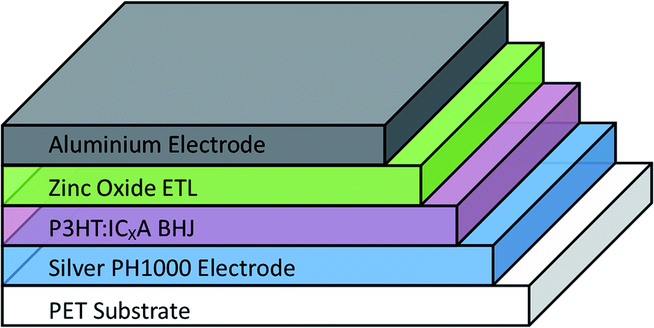 | ||
| Fig. 1 Structure of prepared OPV devices. Solvent annealing was performed immediately after deposition and drying of BHJ, before the zinc oxide ETL was deposited. | ||
2.1 Materials
Materials were used as received unless otherwise stated. Chloroform and methanol were purchased from Sigma-Aldrich. PEDOT:PSS Clevios PH1000 was purchased from Heraeus. The synthesis of P3HT (performed via Grignard metathesis polymerisation) and ICXA were synthesized in house according to literature.11,12 ICXA is a crude mixture of mono-, bis-, and tris-adducted indene C60 which we have reported to be a low cost alternative for common fullerene acceptors such as PCBM.2.2 Deposition
Coating and printing were conducted on a Solar-1 coating line from Grafisk Maskinfabrik using a slot-die head developed at the Technical University of Denmark having a 50 mL ink reservoir volume to ensure uniform ink flow to all stripes or a slot-die head developed to do single stripe slot-die coating.:0.8 weight ratio of P3HT:ICXA and dissolved in chloroform at a solid concentration of 22 mg mL−1. Slot-die coating of the active ink was conducted with a wet thickness of 9 μm. Ovens were set to 50 °C for the purpose of evaporating excess solvent, well below the temperature required for thermal annealing of the active film.12,132.3 Switching
Switching is an electrical activation technique used to burn out electrical shorting through the prepared devices resulting in an improvement of the voltage output of the devices. Switching was conducted by subjecting the device to reverse bias in short pulses using an adjustable power supply with a current of 1 A and a voltage starting at 3 V. The reverse bias magnitude was subsequently increased in 2–3 V steps up to a maximum value of 20 V, which increased the resistance through the device from 2 Ω to 5 kΩ.2.4 J–V measurement
Current density–voltage (J–V) measurements were performed using a sulphur plasma lamp as per previously published work.6 Devices typically had an area of 4 cm2. J–V data was recorded using a Keithley 2400 source meter.2.5 UV-visible spectroscopy (UV-Vis)
UV-Vis of printed cells was performed on a Cary 5000 spectrometer. A baseline measurement was performed using a blank PET substrate. Transmission measurements were taken of solvent annealed and not treated (as printed) films as a percentage relative to the baseline measurements. These measurements were converted to absorbance and normalised at 400 nm.2.6 X-ray diffraction
Glancing incidence X-ray diffraction was performed with a Phillips X'Pert Pro. A cobalt anode (wavelength of 1.79 Å) was used with a voltage of 40 kV and a current of 40 mA. The source was kept at a constant angle of 0.5° while the detector was moved with a step size of 0.05°, scanning for 2 seconds per step.2.7 Fluorescence
Fluorescence measurements were performed using a Shimadzu Fluorimeter with integrating sphere. Calculations of quantum efficiency were performed using methods from the literature.15 The sample was excited at the peak of its adsorption band at 500 nm. Sample light emission was measured between 600 nm and 850 nm.2.8 Photo-CELIV
Photo-CELIV measurements were performed using the PAIOS 2 system (Fluxim AG). Devices were cut from the large area printed cells to a size of ∼0.5 cm2 to reduce the geometric capacitance and allow transient responses to be viewed inside the RC time constant of the equipment. A light pulse from a white LED (Cree, xp-g) was used to generate charges whilst a compensating offset voltage held the device at open circuit. The end of the light pulse was simultaneous with the application of a linearly increasing voltage at a rate of 5 V ms−1 to extract photogenerated charges. The current transients were recorded by the integrated PAIOS hardware. The time resolution of the LED pulse rise was 100 ns, and the calculated RC constant of the devices and measurement system was ≈6 μs.2.9 Transient photovoltage and charge extraction measurements
Transient photovoltage measurements were performed using the PAIOS 2 system (Fluxim AG). The device was illuminated with a high power white LED (Cree, xp-g), the intensity of which was altered by varying the drive current using the PAIOS software to generate various carrier densities. A compensating voltage was supplied to ensure the devices were at open circuit under illumination. A small optical perturbation was generated using a voltage pulse to vary the LED intensity such that the voltage transient had an amplitude of less than 5 mV. The relaxation of the transient voltage back to open circuit following the light pulse was fitted to a monoexponential decay to determine the transient lifetime, which was subsequently adjusted by an experimentally determined factor to calculate the total charge carrier population lifetime as described previously.16 In order to determine the charge density at each illumination level, the time resolved charge extraction technique was applied. This technique involved switching the system from open circuit under illumination to a dark reverse bias of −2 V. The extracted current pulse was integrated in order to provide the charge density initially present in the film under illumination at open circuit.2.10 Capacitance–voltage spectroscopy
Capacitance data was extracted from complex impedance measurements conducted using the PAIOS 2 system (Fluxim AG). The impedance response was measured over the range of 10 Hz to 1 MHz with an oscillation amplitude of 50 mV. The impedance was recorded under dark and illuminated conditions as the applied bias was swept from −4 V to +1 V. The capacitance was determined from the inverse admittance scaled by the angular frequency of the perturbating AC voltage. Devices were illuminated with a white LED (Cree, xp-g) at an intensity of ∼100 mW cm−2 (determined by adjusting the light intensity to give a short circuit current equal to that measured under AM1.5 conditions).2.11 X-ray photoelectron spectroscopy (XPS)
Samples were adhered via a high purity carbon conductive tab (Ted Pella part number: 16084-4). XPS spectra were collected by illuminating the samples with a non-monochromatic X-ray source (Omnivac) using Al Kα (1486.6 eV) radiation, and the photoemission collected by an SES2002 analyser (Scienta). Survey scans were carried out with a pass energy of 200 eV, while regions scans were performed using a pass energy of 20 eV and 100 meV steps. Working pressure in the analysis chamber with sample under X-ray illumination was typically ∼3 × 10⁻⁹ mBar, with a base pressure of 1 × 10⁻⁹ mBar. The relative atomic concentrations corresponding to sulphur bonding environments were determined by peak fitting the S 2p high resolution spectra according to the models established by Greczynski et al.17 and Duvail et al.183 Results
As shown in Fig. 2A, slot-die coating of a solvent mixture, comprising a good solvent (chloroform) and a non-solvent (methanol), was used as the solvent treatment step. Upon coating the chloroform/methanol mixture onto the previously printed active layer (deposited from chloroform at 50 °C), an immediate colour change occurred from the originally printed orange (Fig. 2B) to a red/purple (Fig. 2C); depending on chloroform concentration.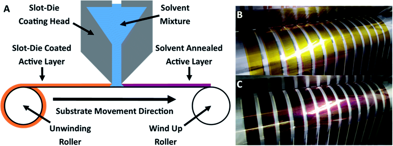 | ||
| Fig. 2 (A) Solvent annealing slot die coating step. (B) Active layer film as printed at the slot die head. (C) Active layer film after solvent annealing with 70% chloroform to 30% methanol mixture at the slot die head. | ||
This colour change is further illustrated in Fig. 3, which shows the difference in colour of the dry active film at the point where solvent annealing was stopped. All of the solvent annealing work in this paper was performed at 0.5 m min−1.
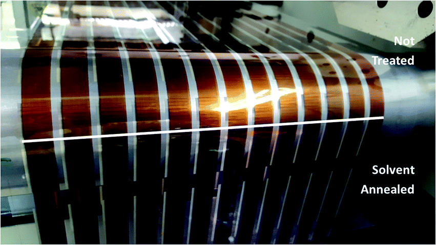 | ||
| Fig. 3 Active film at the point where solvent annealing was stopped. The distinct colour change from unannealed orange (top) to annealed purple (bottom) is visible with a well-defined edge where the solvent flow ceased. | ||
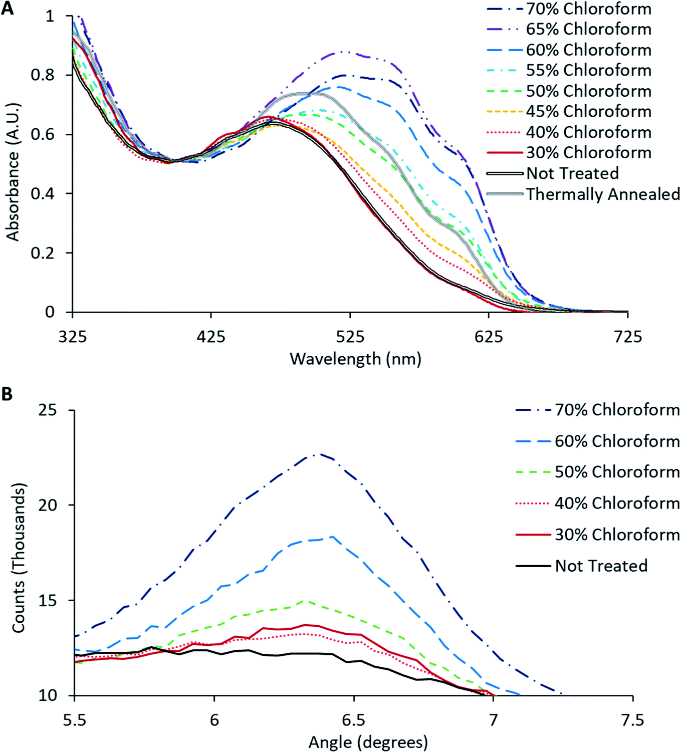
The degree of the solvent induced colour change is determined by the chloroform concentration in the solvent mixture, as shown in Fig. 4. Little to no colour change was observed for solvent mixtures with a chloroform concentration below 40%, 45% to 55% chloroform solvent mixture produced a red hue (typical of films which have undergone thermal annealing at 140 °C for 4 minutes) while chloroform concentrations above 55% resulted in a deep purple active film. These colour changes are typically associated with improved crystallinity of the P3HT;10,19 consistent with the film reordering expected from solvent annealing. In order to confirm this hypothesis, the changes in material packing and crystallinity were investigated by UV-Vis and XRD.
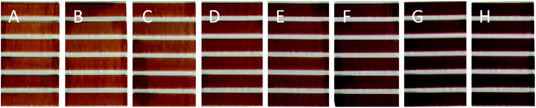 | ||
| Fig. 4 (A) Not treated film printed from chloroform. (B) Film treated with a 40% chloroform solvent mixture. (C) Film treated with a 45% chloroform solvent mixture. (D) Film treated with a 50% chloroform solvent mixture. (E) Film treated with a 55% chloroform solvent mixture. (F) Film treated with a 60% chloroform solvent mixture. (G) Film treated with a 65% chloroform solvent mixture. (H) Film treated with a 70% chloroform solvent mixture. | ||
The crystallinity of P3HT in the active layer was monitored through UV-Vis spectroscopy, where the occurrence of a vibronic peak around 600–620 nm should appear as the degree of crystallinity increases.20 This vibronic shoulder arises due to inter-chain interactions that occur when the P3HT is closely packed in lamellae layered structures that are aligned perpendicular to the substrate. UV-Vis spectra obtained from the solvent annealed films from Fig. 4 (together with the spectrum for a BHJ film thermally annealed at 140 °C for 2 minutes), are shown in Fig. 5A. These UV-Vis spectra show a clear trend as the chloroform fraction increases in the solvent mixture with a distinct shoulder appearing at ∼600–620 nm; indicating polymer ordering associated with an increase in domain size and charge carrier mobility.21 Furthermore, a redshift of the main absorption peak from ∼480 nm to ∼520 nm is observed, indicating an increased intermolecular interaction and improved charge mobility.22
 | ||
| Fig. 5 (A) Normalised UV-Vis absorption of active layer films on PEDOT:PSS/Silver grid electrode. (B) Glancing incidence XRD of active layer films on glass substrate. The thermally annealed sample was annealed at 140 °C for 2 minutes to serve as a comparison to the solvent annealed devices. | ||
The observed increase in crystallinity with increasing chloroform content was verified using glancing incidence XRD of the active layer films; with the intensity of the (1 0 0) peak as a function of chloroform concentration shown in Fig. 5B. This peak has previously been reported to be directly correlated with the degree of crystallinity of P3HT.21 Consistent with the UV-Vis results, the relative intensity of the (1 0 0) peak increases with increasing chloroform content in the solvent mixture, clearly illustrating that there is an increase in the degree of crystallinity in the P3HT as a function of chloroform content in the solvent annealing mixture. Comparing the effect of solvent annealing to thermal annealing, it would appear that the improvement in crystallinity (both vibronic shoulder and redshift) that arises from thermal annealing roughly correlates with that for a film that has been treated with a 50% chloroform solvent mixture. For solvent mixtures above 50% chloroform, the change in film crystallinity for solvent annealing using is actually greater than that due to thermal treatment. Overall, the UV-Vis data reveals that the solvent soaking step does indeed enhance film crystallinity at the microscopic scale.
To fully assess the effectiveness of the solvent soaking at the macroscopic level, OPV devices were prepared. The fabricated device structure was normal geometry with a silver comb coated in PH1000 as the bottom electrode, a P3HT:ICXA active layer, a zinc oxide electron transport layer, and a sputtered aluminium top electrode. All layers were deposited using R2R slot-die coating, with the exception of the silver and aluminium layers which were deposited with R2R flexographic printing and sputter coating, respectively. Solvent annealing (for a range of chloroform fractions) was performed after deposition of the active layer and prior to deposition of the zinc oxide layer.
Device JV curves are presented in Fig. 6. Printed devices were fabricated for reliability as a priority for this study. Given the limits of the coating technique this required substantially thicker active layers than would be typically be optimal for device performance. Printed devices averaged a PCE of 0.08 ± 0.04% which improved to 0.33 ± 0.09% after solvent annealing with a solvent mixture using a chloroform fraction of 30%. As this study is focused on relative performance improvements rising from a processing treatment we have normalised the performance metrics to highlight these relative changes. The comparative device performance as a function of chloroform fraction in the solvent mixture is displayed in Fig. 7. Based on these results a clear peak in device efficiency is found at a chloroform fraction of 30%. Devices prepared with less chloroform in the solvent annealing mixture exhibit lower performance due to reduction in both VOC and JSC, whereas device performances for devices prepared with more than 30% chloroform in the solvent annealing mixture have performance primarily reduced due to a drop in JSC. This result is in contrast to the UV-Vis data, which showed that at a chloroform fraction of 30%, the P3HT crystallinity is significantly lower than for an optimized OPV device prepared with thermal annealing (Fig. 5) and thus the peak in the device performance for solvent annealed devices occurs at sub-optimal P3HT crystallinity.
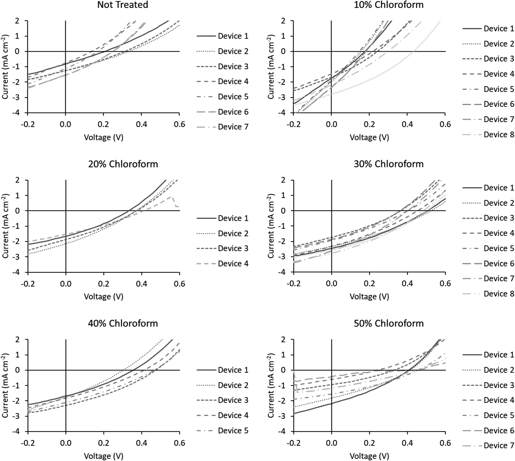 | ||
| Fig. 6 J–V curves for the devices fabricated for this study. Chloroform fraction in the solvent annealing mixture is indicated above the chart. | ||
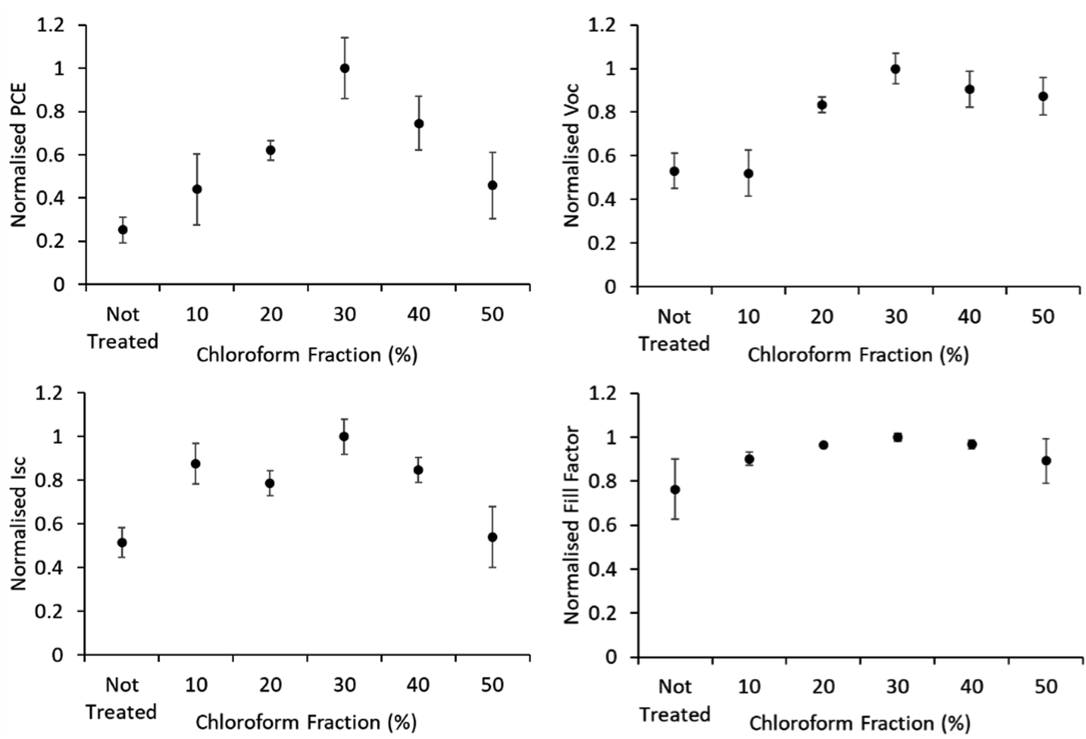 | ||
| Fig. 7 IV characteristics of solvent annealed devices. Error bars are standard deviation among the 4–9 R2R devices produced for each test. | ||
Photo-CELIV measurements (Fig. 8) reveal that the charge carrier mobility improves with greater chloroform concentration in the solvent mixture from ∼2.5–10 × 10−6 V2 cm−1 s−1, when increasing the chloroform fraction from 0 to 50%. This increased mobility arises from an increase in either the degree of crystallinity of the polymer phase or the size of the crystalline domains, consistent with the conclusions from the shift in UV-Vis spectra and XRD of the films presented in Fig. 5. This increasing mobility is consistent with the observed improvement in the solvent annealed device PCE for chloroform fractions of 0–30%, as charge extraction becomes more efficient. However, the increased mobility does not correlate with the decreased PCE observed for chloroform fractions >30%; indicating that another mechanism must be dominant in these devices.
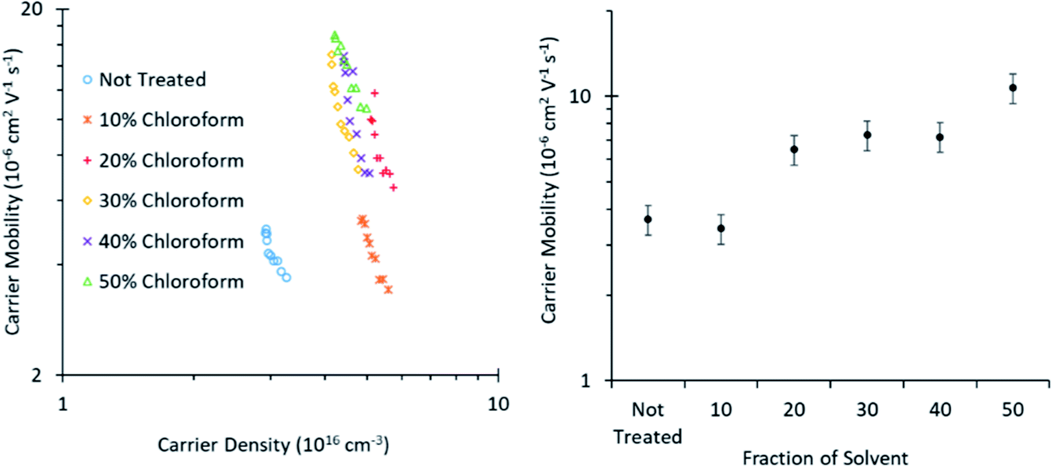 | ||
| Fig. 8 Charge carrier mobility as calculated from Photo-CELIV measurements of roll-to-roll printed OPVs cut to a small size appropriate to the measurement technique. | ||
Fluorescence measurements were conducted to determine the charge separation of various single material, blended, and annealed films, shown in Fig. 9 and Table 1. The fluorescence signal arises from radiative relaxation of the polymer excited state. In blended films, charge separation of the polymer excitons results in a non-radiative loss of the polymer excited state, leading to a reduction in the fluorescence signal. Accordingly comparing the fluorescence intensity from blended films to that of pure polymer films (corrected for light intensity adsorbed at the excitation wavelength) provides insight into the charge separation efficiency.15 The untreated active film exhibits the lowest fluorescence yield (and hence the highest charge separation) consistent with the observed low polymer crystallinity (and consequent poor charge mobility). For the solvent annealed films, charge separation exhibits a maximum (fluorescence yield minimum) at a chloroform fraction of 30%. While the trend in the fluorescence quantum efficiency (FQE) and PCE as a function of chloroform fraction are qualitatively correlated, the magnitude of the FQE change (Table 1) cannot entirely explain the change in PCE.
 | ||
| Fig. 9 Measurement of fluorescence of various films after exposure to a 500 nm light source. Measured include BHJ films treated with the solvent annealing mixture, BHJ films not treated, and a pure P3HT film. (A & B) show the same dataset with different scales. | ||
| Sample | Fluorescence quantum efficiency |
|---|---|
| Not treated | 4.21 × 10⁻⁵ |
| 10% chloroform/90% methanol | 1.11 × 10⁻⁴ |
| 20% chloroform/80% methanol | 1.05 × 10⁻⁴ |
| 30% chloroform/70% methanol | 1.02 × 10⁻⁴ |
| 50% chloroform/50% methanol | 1.19 × 10⁻⁴ |
| 60% chloroform/40% methanol | 1.38 × 10⁻⁴ |
| P3HT | 3.00 × 10⁻³ |
To further probe the origin of the observed PCE behaviour with changing chloroform fraction, the charge carrier lifetime was monitored using transient photovoltage measurements (Fig. 10). These measurements exhibited the typical power law dependence on charge carrier density, although the slope of the curves was greater than typically expected and did not return physically sensible reaction orders for recombination, which are typically in the range of 2–3 for P3HT:PCBM OPV devices.23 The gradient in the lifetime plots is strongly influenced by the large area of the roll-to-roll printed devices, which exhibit substantial geometric capacitance and thus prevent lifetime measurements on a time scale shorter than ∼10 μs. It is therefore suspected that there is substantial charge leakage due to recombination during this time period when attempting to measure the charge density and, as such, the lifetime gradients are not reliable indicators of the recombination reaction order and the charge carrier lifetime values may not be quantitatively accurate. However, as the slopes are comparable in value, indicating a similar recombination mechanism for all devices, relative comparisons between device treatment conditions are still valid.
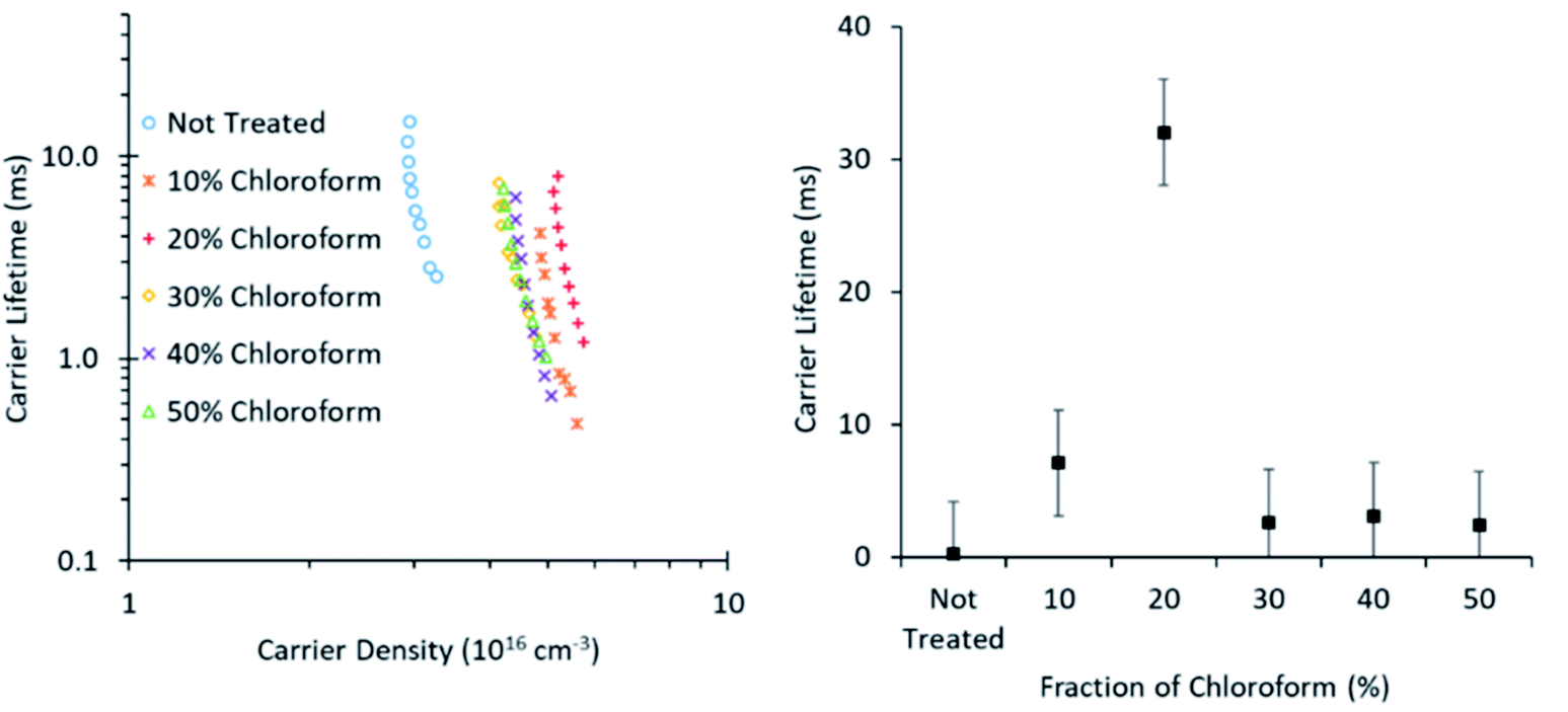 | ||
| Fig. 10 Charge carrier lifetime as influenced by carrier density (left) and chloroform amount in the solvent mixture at 4.5 × 1016 cm−3 (right). Data was collected using TRCE measurements. | ||
The lifetime values from Fig. 10 indicate that the charge carrier lifetime peaks at a chloroform fraction of 20% chloroform concentration. When combining this observation with the trend in the mobility measurements to provide a μτ product indicative of charge extraction, the product shows the same trend as the device PCE. The μτ trend indicates that it is enhanced recombination that creates the performance limit on devices as the solvent annealing treatment is switched to higher chloroform fractions. This explanation for the dominant charge carrier behaviour influencing device performance was verified using capacitance voltage spectroscopy (Fig. 11). The data indicates a minimum capacitance at reverse bias values of −2 to −3 V, suggesting that there is substantial recombination at short circuit present in all devices. The geometric capacitance at −4 V suggests a dielectric constant of the devices in the range of 3.3–3.6; consistent with previous reports for the same active layer materials.24
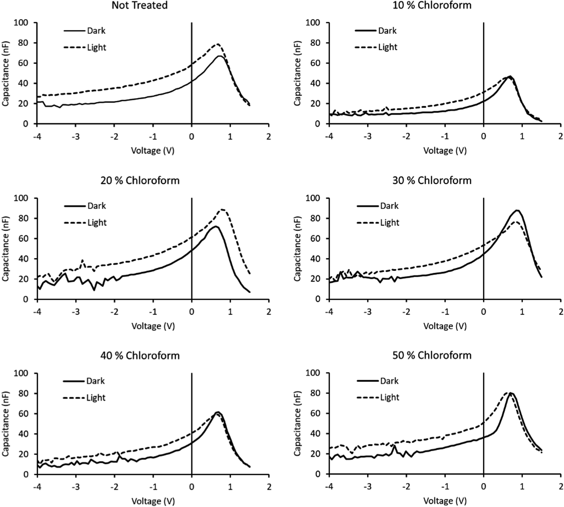 | ||
| Fig. 11 Capacitance–voltage spectroscopy curves of solvent annealed devices, both in the dark and under illumination. Fraction of chloroform in the solvent mixture indicated above chart. | ||
By removing the dark scans from the illuminated scans, the capacitance reflective of the photogenerated charge can be obtained. A comparison of the integrated photogenerated charge from reverse bias to short circuit conditions indicates the total built up charge that remains unextracted at this circuit condition. By comparing this value to the same process, but continuing the integration from reverse bias to open circuit conditions, a measure of the charge remaining at short circuit to the total charge generated at open circuit is created. Subtracting this ratio from unity provides a measure of the charge collection efficiency with a maximum observed for the 30% chloroform treatment case, verifying the findings from transient measurements that the charge collection efficiency is the underlying origin of the observed device PCE results with varying chloroform treatment (Table 2).
| Chloroform ratio (%) | VOC (V) | Q(V=0) (nC) | Q(V=Voc) (nC) | ηcoll (%) |
|---|---|---|---|---|
| Not treated | 0.691 | 72.0 | 106.7 | 32.5 |
| 10 | 0.696 | 32.3 | 47.4 | 31.9 |
| 20 | 0.715 | 88.3 | 128.2 | 31.1 |
| 30 | 0.712 | 51.0 | 80.3 | 36.5 |
| 40 | 0.690 | 53.8 | 83.0 | 35.3 |
| 50 | 0.683 | 65.5 | 100.2 | 34.7 |
One possible cause of the enhanced recombination observed with the transient photo voltage measurements is that the methanol in the solvent mixture causes material dissolved in the slot-dye meniscus to deposit into larger than expected domain sizes for the corresponding P3HT crystallinity; decreasing charge separation without observing an over annealing in the UV-Vis spectra. However, if the larger domain sizes were the cause of the PCE decrease for chloroform fractions >30% then a greater difference in measured quantum efficiencies between samples would be expected. Alternatively, it is the condition of the active layer surface after solvent annealing that is the driving mechanism for the peak in PCE for a chloroform fraction of 30%.
The condition of the surface of the active layer was investigated with AFM before and after solvent annealing. The AFM micrographs (Fig. 12) show a largely featureless bulk heterojunction film prior to any solvent annealing treatment. Sub-micrometre sized peaks are visible after treatment with the 30% chloroform fraction solvent annealing mixture, and after treatment with the 50% chloroform fraction mixture troughs are apparent of the same size and density of the peaks seen in the 30% case. As such, the AFM images indicate that annealing with a solvent mixture of 30% chloroform/70% methanol causes aggregate formation in the active film. At higher chloroform concentrations, these aggregates are washed away to create pinholes which are responsible for the increased charge recombination, resulting in a lower JSC. To support this hypothesis further, XPS was performed on films pre- and post solvent annealing.
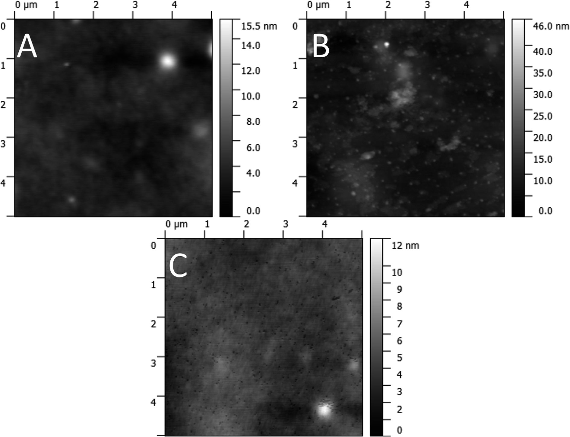 | ||
| Fig. 12 AFM images of the active layer before top electrode application. (A) Untreated active layer. (B) Active layer after treatment with 30% chloroform/70% methanol solution. (C) Active layer after treatment with 50% chloroform/50% methanol solution. | ||
XPS measurements of the active film (Fig. 13A) reveal that, as chloroform increased in the solvent annealing mixture, the observed carbon content decreased but sulphur and oxygen content increased. Peak fitting to the S 2p region scan (Fig. 13B) reveals more specific information concerning the nature of the change in sulphur signal. The not treated film has no signal indicative of PSS bonding environments; rather, the spectra is made up of contributions from thiophene species (namely the P3HT and PEDOT, with the latter likely the primary source for the doped thiophene signature). On application of the solvent annealing treatment, the thiophene contribution drops, while a PSS contribution appears at higher binding energies. Methanol is a known PSS solvent25 and, as it is being used in the solvent annealing mixture, it is possible that the PSS is being brought to the surface of the active layer during this process.
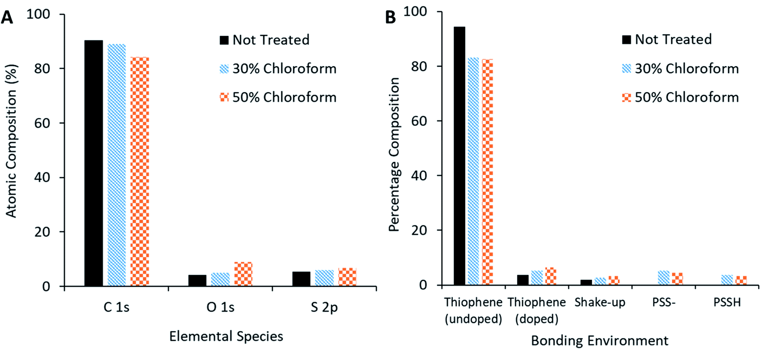 | ||
| Fig. 13 XPS compositional analysis of solvent annealed active layer. (A) Comparison of species present on surface of active film. (B) Bonding environment on surface of active film. | ||
The device stack used for device fabrication applies an electron transport layer (ETL) after the solvent treatment step and any hole transport layer (HTL)–ETL interfaces formed would prevent charge extraction through the top electrode.
To further elucidate the effect of solvent annealing on the active layer surface structure, XPS measurements were repeated with bulk heterojunction films being printed on an aluminium film, rather than a PEDOT:PSS film. As neither chloroform nor methanol are solvents for aluminium any increase in the XPS aluminium signal on the active film surface at high chloroform fractions would be a signature that pinholes are forming in the active film surface. The XPS data in Fig. 14 reveals that, indeed, a greater degree of aluminium is present on the sample surface after treatment with a solvent mixture of 50% chloroform/50% methanol then either the solvent mixture of 30% chloroform/70% methanol or not treated cases, consistent with pinhole formation. Thus it would appear that it is the formation of pinholes in the active film surface, possibly with enhanced PSS diffusion to the surface, which provides a pathway for the observed increase in charge recombination (resulting in a decrease in JSC and therefore PCE) at chloroform fraction >30%.
 | ||
| Fig. 14 (A) XPS compositional analysis of solvent annealed active layer printed on an aluminium substrate. (B) XPS bonding environment analysis of solvent annealed active layer printed on an aluminium substrate. | ||
4 Conclusion
A novel solvent annealing based pathway for the preparation of OPVs on the R2R scale that is compatible with substrates, such as canvas and fabric, which are not able to withstand the high temperatures normally used in OPV production has been investigated. Solvent soaking of printed P3HT:ICxA films with a mixture of chloroform and methanol is shown to have a significant effect on the P3HT crystallinity, which increases systematically as a function of chloroform fraction in the solvent annealing mixture. This increase was evident both from glancing incidence X-ray diffraction and UV-Vis where a clear colour change going from yellow to deep purple was demonstrated. Applying these films to OPV devices increases device performance by a factor of 4 above the non-annealed film was observed in the 30% chloroform/70% methanol case. This increase in device performance is attributed to increasing P3HT conjugation length and crystallinity which improves the charge carrier mobility of the active film. However, at chloroform concentrations above 30% in the solvent soaking mixture, device JSC decreases; limiting device performance. Charge transport measurements show that this performance decrease cannot be attributed to the charge mobility but instead arises from charge recombination due to changes in surface morphology. AFM and XPS measurements confirm that it is the formation of pinholes in the active film with increasing chloroform fraction in the solvent mixture that drives the higher charge recombination observed at choloroform fractions >30%. As such, this work provides the basis for further studies of different solvent mixtures and soaking conditions that will enable improved device performance without detrimentally impacting surface morphology.
Conflicts of interest
There are no conflicts to declare.Acknowledgements
The work was also performed in part at the Materials node of the Australian National Fabrication Facility, a company established under the National Collaborative Research Infrastructure Strategy to provide nano and microfabrication facilities for Australia's researchers. Authors gratefully acknowledge funding support from the Australian Research Council through its Discovery Project scheme (DP170102467). This research is supported by an Australian Government Training Program (RTP) Scholarship.References
- G. Dennler, M. C. Scharber and C. J. Brabec, Polymer-Fullerene Bulk-Heterojunction Solar Cells, Adv. Mater., 2009, 21(13), 1323–1338 CrossRef CAS
.
- C. J. M. Emmott, A. Urbina and J. Nelson, Environmental and economic assessment of ITO-free electrodes for organic solar cells, Sol. Energy Mater. Sol. Cells, 2012, 97, 14–21 CrossRef CAS
- F. C. Krebs, T. Tromholt and M. Jorgensen, Upscaling of polymer solar cell fabrication using full roll-to-roll processing, Nanoscale, 2010, 2(6), 873–886 RSC
- M. Pagliaro, R. Ciriminna and G. Palmisano, Flexible solar cells, ChemSusChem, 2008, 1(11), 880–891 CrossRef CAS PubMed
- R. Mather and J. Wilson, Fabrication of Photovoltaic Textiles, Coatings, 2017, 7(5), 63 CrossRef
- T. R. Andersen, et al., Comparison of inorganic electron transport layers in fully roll-to-roll coated/printed organic photovoltaics in normal geometry, J. Mater. Chem. A, 2016, 4(41), 15986–15996 RSC
- U. Zhokhavets, et al., Effect of annealing of poly(3-hexylthiophene)/fullerene bulk heterojunction composites on structural and optical properties, Thin Solid Films, 2006, 496(2), 679–682 CrossRef CAS
- J. Nelson, Polymer:fullerene bulk heterojunction solar cells, Mater. Today, 2011, 14(10), 462–470 CrossRef CAS
- Y. Zhao, et al., Solvent-vapor treatment induced performance enhancement of poly(3-hexylthiophene):methanofullerene bulk-heterojunction photovoltaic cells, Appl. Phys. Lett., 2007, 90, 043504 CrossRef
- H. Li, et al., Solvent-soaking treatment induced morphology evolution in P3HT/PCBM composite films, J. Mater. Chem., 2011, 21, 6563–6568 RSC
- T. M. Pappenfus, et al., Exploration of the Direct Arylation Polymerization Method for the Practical Application of Conjugated Materials: Synthetic Scale-Up, Solar Cell Performance, and Cost Analyses, Macromol. Chem. Phys., 2018, 219(21), 1800272 CrossRef
- N. A. Cooling, et al., A low-cost mixed fullerene acceptor blend for printed electronics, J. Mater. Chem. A, 2016, 10274–10281 RSC
- T. R. Andersen, et al., Fully roll-to-roll prepared organic solar cells in normal geometry with a sputter-coated aluminium top-electrode, Sol. Energy Mater. Sol. Cells, 2016, 149, 103–109 CrossRef CAS
- F. C. Krebs, Air stable polymer photovoltaics based on a process free from vacuum steps and fullerenes, Sol. Energy Mater. Sol. Cells, 2008, 92(7), 715–726 CrossRef CAS
- J. C. d. Mello, H. F. Wittmann and R. H. Friend, An improved experimental determination of external photoluminescence quantum efficiency, Adv. Mater., 2004, 9(3), 230–232 CrossRef
- B. C. O'Regan, et al., Influence of the TiCl4 Treatment on Nanocrystalline TiO2 Films in Dye-Sensitized Solar Cells. 2. Charge Density, Band Edge Shifts, and Quantification of Recombination Losses at Short Circuit, J. Phys. Chem. C, 2007, 111(37), 14001–14010 CrossRef
- G. Greczynski, et al., Photoelectron spectroscopy of thin films of PEDOT–PSS conjugated polymer blend, J. Electron Spectrosc. Relat. Phenom., 2001, 121(1–3), 1–17 CrossRef CAS
- J. L. Duvail, et al., Effects of the Confined Synthesis on Conjugated Polymer Transport Properties, J. Phys. Chem. B, 2004, 108(48), 18552–18556 CrossRef CAS
- S. Sun, et al., A new insight into controlling poly(3-hexylthiophene) nanofiber growth through a mixed-solvent approach for organic photovoltaics applications, J. Mater. Chem., 2011, 21(2), 377–386 RSC
- Y. Kim, et al., A strong regioregularity effect in self-organizing conjugated polymer films and high-efficiency polythiophene:fullerene solar cells, Nat. Mater., 2006, 5(3), 197–203 CrossRef CAS
- F.-C. Chen, et al., Morphological study of P3HT:PCBM blend films prepared through solvent annealing for solar cell applications, Sol. Energy Mater. Sol. Cells, 2010, 94(12), 2426–2430 CrossRef CAS
- U. Zhokhavets, et al., Relation between absorption and crystallinity of poly(3-hexylthiophene)/fullerene films for plastic solar cells, Chem. Phys. Lett., 2006, 418(4–6), 347–350 CrossRef CAS
- C. G. Shuttle, et al., Bimolecular recombination losses in polythiophene: Fullerene solar cells, Phys. Rev. B, 2008, 78(11), 113201 CrossRef
- B. J. Leever, et al., In Situ Characterization of Lifetime and Morphology in Operating Bulk Heterojunction Organic Photovoltaic Devices by Impedance Spectroscopy, Adv. Energy Mater., 2012, 2(1), 120–128 CrossRef CAS
- D. Alemu, et al., Highly conductive PEDOT:PSS electrode by simple film treatment with methanol for ITO-free polymer solar cells, Energy Environ. Sci., 2012, 5(11), 9662–9671 RSC
| This journal is © The Royal Society of Chemistry 2019 |