
 Open Access Article
 This Open Access Article is licensed under a Creative Commons Attribution-Non Commercial 3.0 Unported Licence
Structure of Ni(OH)2 intermediates determines the efficiency of NiO-based photocathodes – a case study using novel mesoporous NiO nanostars†
Ruri Agung Wahyuonoab,
Andrea Dellitha,
Christa Schmidta,
Jan Dellitha,
Anna Ignaszak c,
Martin Seyringd,
Markus Rettenmayrd,
Jennifer Fizee,
Vincent Arteroe,
Murielle Chavarot-Kerlidoue and
Benjamin Dietzek*abf
c,
Martin Seyringd,
Markus Rettenmayrd,
Jennifer Fizee,
Vincent Arteroe,
Murielle Chavarot-Kerlidoue and
Benjamin Dietzek*abf
aLeibniz Institute of Photonic Technology (IPHT), Department Functional Interfaces, Jena e. V. Albert-Einstein-Str. 9, 07745 Jena, Germany. E-mail: benjamin.dietzek@ipht-jena.de
bInstitute for Physical Chemistry and Abbe Center of Photonics, Friedrich Schiller University Jena, Helmholtzweg 4, 07743 Jena, Germany
cDepartment of Chemistry, University of New Brunswick, 30 Dineen Drive (Toole Hall Room 122), Fredericton, NB, E3B 5A3 Canada
dOtto Schott Institute of Materials Research (OSIM), Friedrich Schiller University Jena, Löbdegraben 32, 07743 Jena, Germany
eUniv. Grenoble Alpes, CNRS, CEA, IRIG, Laboratoire de Chimie et Biologie des Métaux, 38000 Grenoble, France
fCenter for Energy and Environmental Chemistry (CEEC Jena), Friedrich Schiller University Jena, Philosophenweg 7a, 07743 Jena, Germany
First published on 29th November 2019
Abstract
We report the wet chemical synthesis of mesoporous NiO nanostars (NS) as photocathode material for dye-sensitized solar cells (DSSCs). The growth mechanism of NiO NS as a new morphology of NiO is assessed by TEM and spectroscopic investigations. The NiO NS are obtained upon annealing of preformed β-Ni(OH)2 into pristine NiO with low defect concentrations and favorable electronic configuration for dye sensitization. The NiO NS consist of fibers self-assembled from nanoparticles yielding a specific surface area of 44.9 m2 g−1. They possess a band gap of 3.83 eV and can be sensitized by molecular photosensitizers bearing a range of anchoring groups, e.g. carboxylic acid, phosphonic acid, and pyridine. The performance of NiO NS-based photocathodes in photoelectrochemical application is compared to that of other NiO morphologies, i.e. nanoparticles and nanoflakes, under identical conditions. Sensitization of NiO NS with the benchmark organic dye P1 leads to p-DSSCs with a high photocurrent up to 3.91 mA cm−2 whilst the photoelectrochemical activity of the NiO NS photocathode in aqueous medium in the presence of an irreversible electron acceptor is reflected by generation of a photocurrent up to 23 μA cm−2.
Introduction
Solar irradiation provides a power of 1.2 ×10⁵ TW, i.e. a massive and clean energy source for fueling the worldwide power demand of currently 12 TW.1 Therefore, solar energy conversion systems exploiting the third-generation solar cell technology have gained significant interest offering low-cost fabrication and yielding relatively high efficiency.1–4 In particular, sensitization of thin film n-type metal oxide semiconductor photoanodes, e.g. TiO2, in the form of dye-sensitized solar cells (n-DSSCs), has continuously improved yielding power conversion efficiencies (PCE) beyond 10%.1,2 In order to build tandem-DSSCs, p-type semiconductor photocathodes (p-DSSCs) based on NiO have been researched. In contrast to n-DSSC whose charge separation occurs upon electron injection from the excited state of dye sensitizer to the conduction band (CB) of the semiconductor, in p-DSSC1,3 a hole is injected from the excited state of the photosensitizer into the valence band (VB) of the semiconductor (Dye*|NiO + hν → Dye−|NiO(h+)) to create charge separation and to generate a photocathodic current.4,5Seminal work on p-DSSCs was reported by Hagfeldt in 1999, achieving PCE of 0.0076% using a tetrakis(4-carboxyphenyl)-porphyrin-sensitized NiO photocathode.4 While n-type DSSC have matured into a robust technology awaiting commercialization, the photocathode remains subject of optimization.5 Their low performance compared to photoanodes hinders e.g. the design of tandem DSSC (t-DSSC) which theoretically can break the Shockley–Queisser (SQ) limit.5–7 Nonetheless, the development of dye-sensitized photocathodes has also inspired the design of dye-sensitized photoelectrochemical cells (DSPECs) providing an attractive alternative for direct solar energy conversion and storage into the form of a fuel such as hydrogen8–15 or CO2 reduction products.16,17
Recent studies suggest that achieving high-performance p-DSSC should address the low hole mobility in p-semiconductor, the fast geminate recombination, the high dark current density, high series resistance and low shunt resistance.5–12 As mentioned above, NiO (Eg = 3.7–3.9 eV) which exhibits good transparency in the wavelength range of the absorption of common photosensitizers13–19 is the almost exclusively used material in p-DSSC although other wide-band gap p-type semiconductors have been explored, e.g. copper-based delafossites, copper oxides, and cobalt oxides.20–27 The main challenges in using NiO are its high valence band (VB) potential (0.54 V vs. NHE), thus limiting the maximum voltage generated in a DSSC, and the poor hole mobility.5,15–17 These properties of NiO originate from a vast amount of inherent defects, such as oxygen- and nickel-site defects, due to the non-stoichiometric conditions in NiO.5,28–31 These defects, which are reflected in the absorption spectrum of NiO, create localized electronic states in the band gap and act as trap states which cause charge recombination at the NiO-photosensitizer interface.37–40 In order to reduce the defects in NiO, modifications of the synthetic routes or post-treatment have been suggested. It has been shown that modifying the structural properties of metal-oxide semiconductor alters the electronic energy levels in semiconductors by modifying interatomic distances and hence, affects its functionality.28–30
Here we report a novel NiO nanostructure, i.e. porous NiO nanostars, fabricated by wet chemical synthesis. The growth and formation mechanism of these NiO nanostars are discussed based on a combination of electron microscopy and Raman scattering. The NiO nanostars are evaluated as materials for photocathodes in DSSCs and DSPECs and their structure and performance are compared to other NiO morphologies conventionally employed in NiO-based photocathodes. We show that NiO prepared via β-Ni(OH)2 displays superior performance in terms of photoelectrochemical characteristics compared to NiO samples prepared via α-Ni(OH)2. Thus, the results presented here provide key information for the design of synthetic routes in wet chemical synthesis of NiO for photocathode materials.
Experimental Section
Synthesis of NiO nanostructures
For synthesizing porous NiO nanostars (NS), 1 mmol of NiCl2·6H2O (Sigma Aldrich) and 0.04 mmol of Na2C2O4 (Sigma Aldrich) were dissolved into 30 mL mixture of diethyleneglycol (DEG) and water (2![[thin space (1/6-em)]](https://www.rsc.org/images/entities/char_2009.gif) :1% v/v) and stirred at 50 °C for 15 min. The reaction mixture was then heated to 225 °C and stirred for 12 h until a light blue precipitate was obtained. The precipitate was annealed at 450 °C for 2 h to obtain NiO NS.
:1% v/v) and stirred at 50 °C for 15 min. The reaction mixture was then heated to 225 °C and stirred for 12 h until a light blue precipitate was obtained. The precipitate was annealed at 450 °C for 2 h to obtain NiO NS.
Synthesis of compact NiO nanoparticles (NP) was carried out by preparing 0.1 M of Ni(CH3COOH)2·2H2O (Sigma Aldrich) in diethyleneglycol (DEG) and heating at 180 °C. Once the reaction temperature reached 150 °C, 10 mL of distilled water were injected and the solution was stirred for 2 h. A green solution was obtained and cooled down in a flask and centrifuged. The reaction solution was annealed at 450 °C for 2 h to obtain NiO NP. Synthesis of NiO nanoflakes (NF) was carried out by dissolving 2.5 g NiSO4 and 0.5 g potassium persulfate 6H2O (Carl Roth GmbH & Co. KG) into 200 mL distilled water and subsequent stirring at 50 °C for 15 min. An amount of 2.5 mL NH4OH was added dropwise to the solution. The solution turned dark blue and eventually became black. The black precipitate was filtered and washed with distilled water several times to remove excess ammonium, and annealed at 450 °C for 2 h to obtain NiO NF.
Characterizations
NiO nanostructures were investigated with field emission scanning electron microscopy (FESEM, JEOL JSM6300F) operating at 5 kV. Transmission electron microscopy (TEM) and high-resolution transmission electron microscopy (HRTEM) were carried out using a JEOL JEM-3010HT equipped with a LaB6 cathode operating at 300 kV. Crystal structures were determined by powder X-ray diffraction (XRD) with a PANalytical X'pert diffractometer (40 kV, 40 mA). Diffraction patterns were obtained for 15°–70° (2θ) by step scanning with a step size of 0.02° using both Cu Kα1 (transition KLIII; λ = 1.54056 Å) and Cu Kα2 lines (transition KLII; λ = 1.54439 Å). The diffraction data were Rietveld-refined for further analysis. FT-IR transmission spectra were measured on a Thermo Scientific Nicolet iS10. Raman spectra were collected using an electrically cooled spectrometer (Raman-HR-TEC, StellarNet) and a diode laser for excitation at 785 nm. All the measurements were performed in triplicate. For TGA/DSC measurements (Mettler Toledo Star-e) 12 mg of NiO were placed in a crucible under N2 atmosphere and heated from 36 to 1000 °C at a heating rate of 10 K min−1. Specific surface areas of NiO were determined by multipoint BET (Brunauer–Emmett–Teller) tests under N2 atmosphere (Autosorb-1, Quantachrome) at 77 K. The NiO samples were heated at 350 °C for evaporating the surface water prior to the physisorption test. Optical properties of NiO were characterized by absorption and emission spectroscopy employing a Varian Cary 5000 spectrometer. Cyclic voltammetry and impedance measurement of NiO were carried out using computer controlled potentiostat-galvanostat (Princeton Applied Research VersaSTAT) in three electrode system using 0.2 M KCl as the supporting electrolyte and 0.01 M KH2PO4 and 0.01 M K2HPO4 as the buffer (details in ESI†).Preparation of NiO photocathodes and dye-loading test
NiO photocathodes are prepared by doctor blading of NiO paste consisting of NiO powders, ethyl cellulose and terpineol (weight ratio of 1:5:10) onto FTO substrates and subsequently annealing at 450 °C. Different dyes bearing different anchoring groups were used for sensitization,32–34 i.e. Ru1 ([Ru(bpy)2dppz](PF6)2 with phosphonic acid anchoring groups), Ru2 (tris[4,4′-bis(ethylcarboxy)-2,2′-bipyridine]Ru(II) dihexafluorophosphate, [Ru(dceb)3](PF6)2), Cu1 (Cu(I) 4H-imidazolate complex with a pyridine anchoring group), P1 (4-(Bis-{4-[5-(2,2-dicyano-vinyl)-thiophene-2-yl]-phenyl}-amino)-benzoic acid) or Coumarin 343 (see Fig. 5). While P1 (Dyenamo) and Coumarin 343 (Sigma Aldrich) were purchased, Ru1, Ru2, and Cu1 were synthesized and prepared from the previous studies.41–43 The NiO electrodes were soaked in a 0.5 mM solution of dye in acetonitrile for 24 h. To estimate the amount of dye chemisorbed on the NiO photocathode (dye-loading), the dye-sensitized NiO photocathode was immersed in a 1 M NaOH solution in a water:ethanol mixture (1:1 v/v) for 2 h, resulting in the desorption of the dye molecules.35 The absorbance of the resulting solution was measured and the amount of desorbed dye was determined by comparing the absorbance of the desorbed solution at the absorption maximum with the absorbance of a reference UV/vis spectrum of a known concentration of the dye (also in 1 M NaOH solution with water and ethanol mixture (1:1 v/v)).
NiO based-DSSCs
For DSSCs fabrication, NiO electrodes were sensitized in a 0.5 mM solution of Ru2, P1 and Coumarin 343 for 24 h. The redox couple I3−/I−, containing 0.5 M tert-butylammonium iodide, 0.1 M lithium iodide, 0.1 M iodine and 0.5 M 4-tert-butylpyridine, was used as electrolyte. Platinized FTO was utilized as counter electrode. Sandwiched DSSCs were built using surlyn polymer (Meltonix 1170-60, SOLARONIX) as a spacer. The solar cell properties were characterized by current–voltage (I–V) measurements under 100 mW.cm−2 irradiation using a solar simulator (SS-80 PET) equipped with an AM1.5 filter. The open circuit voltage decay (OCVD) measurements were carried out under the same solar simulator and the voltage decay was recorded once the solar cell generated a steady state voltage and the illumination source was turned off. The trap-state densities were fit according to chemical capacitance-based model.36,37Photoelectrochemical activity assessment of the NiO photocathodes
Photocurrent measurements were performed in a specific electrochemical cell in a three-electrode configuration, using the different NiO films sensitized with the organic push–pull dye T1 (((E)-4,40-((4-(5-(2-cyano-3-ethoxy-3-oxoprop-1-en-1-yl)thiophen-2-yl)phenyl)aza-nediyl)dibenzoic acid)).38,39 For comparison, T1-sensitized commercial NiO films (two layers, screen-printed onto conductive glass) purchased from Dyenamo AB (Stockholm, Sweden) were employed. The surface of the working electrode in contact with the electrolyte was 0.24 cm2. Ti wire and Ag/AgCl were used as counter and reference electrodes, respectively. [Co(NH3)5Cl]Cl2 (20 mM) was used as irreversible electron acceptor in a sodium acetate buffer (0.1 M, pH 4.5) solution as electrolyte. Photoelectrodes were back-illuminated with a 300 W ozone-free xenon lamp (Newport) operated at 280 W coupled to a water-filled Spectra-Physics 6123NS liquid filter for elimination of IR radiation and a Spectra-Physics 59472 UV cut-off filter (λ > 400 nm). Irradiance at the substrate surface was adjusted to 50 mW cm−2 (ca one sun on the 400–800 nm range) using a Newport PM1918-R powermeter.Results and discussion
Growth mechanism and microstructural properties of NiO nanostars
The growth mechanism as well as the self-assembly of the NiO nanostars is discussed based on TEM data and Raman spectra (Fig. 1). Elucidating the nucleation state and growth of NiO NS is important for the optimization of self-assembled NiO nanostructures and their microstructural and physical properties. Five different solutions were monitored by Raman spectroscopy at various times to investigate the different states within the synthesis and to unravel the growth mechanism of NiO NS. In the synthesis NiCl2 and Na2C2O4 are first hydrolyzed and deionized. The resultant Ni2+ ions can react with C2O42− yielding NiC2O4·xH2O40 and Ni(OH)2.41 The increasing Raman signals (Fig. 1a) of nickel(II) oxalate at 520, 601, 1415, and 1635 cm−1 are assigned to Ni–O–C deformation, O–C–O deformation, symmetric C–C and O–C–O deformation, and H–O–H as well as C–C–O deformation, respectively.41 The presence of Ni(OH)2 is indicated by the Raman signals at 605 and 880 cm−1.42 Dehydration and nucleation starts after 5 h. This process can be observed as the Raman signal at 1635 cm−1 (corresponding to H–O–H deformation) vanishes. The resultant nuclei have sizes ranging from 3.6 to 7.5 nm. After nucleation, a mixture of Ni(OH)2, NiO and excess NiCl2 is observed as indicated by the intensity profile of selected area diffraction pattern (SAD, Fig. 1b). This observation is further supported by the HRTEM and fast Fourier transform (FFT) analyses (Fig. 1c and d), which shows the interplanar spacing of 0.299 and 0.237 nm for (100) and (101) lattice diffraction fringes of Ni(OH)2, respectively, and the interplanar spacing of 0.207 and 0.240 nm for the (200) and (111) diffraction fringes of NiO, respectively. The NiO precipitates obtained in the end of synthesis reaction shows pristine NiO with higher crystallinity as a result of completely grown NiO yielding particles with size ranging from 10 and 21 nm. This higher crystallinity is also indicated by the sharp diffraction spots in the FFT images (Fig. 1e). Furthermore, it should be noted that the observed Ni(OH)2 during nucleation and growth shows β phase (see illustration in Fig. 1f to distinguish β and α phase of Ni(OH)2). These particles in turn self-assemble into star-shape structures consisting fibers/rods. Finally, crystalline NiO NS are obtained by annealing the resultant NiC2O4 and Ni(OH)2 above the phase transformation temperature, i.e. 225 °C as indicated by DSC curve (vide infra). The growth and formation mechanism of NiO NS is schematically illustrated in Fig. 1g.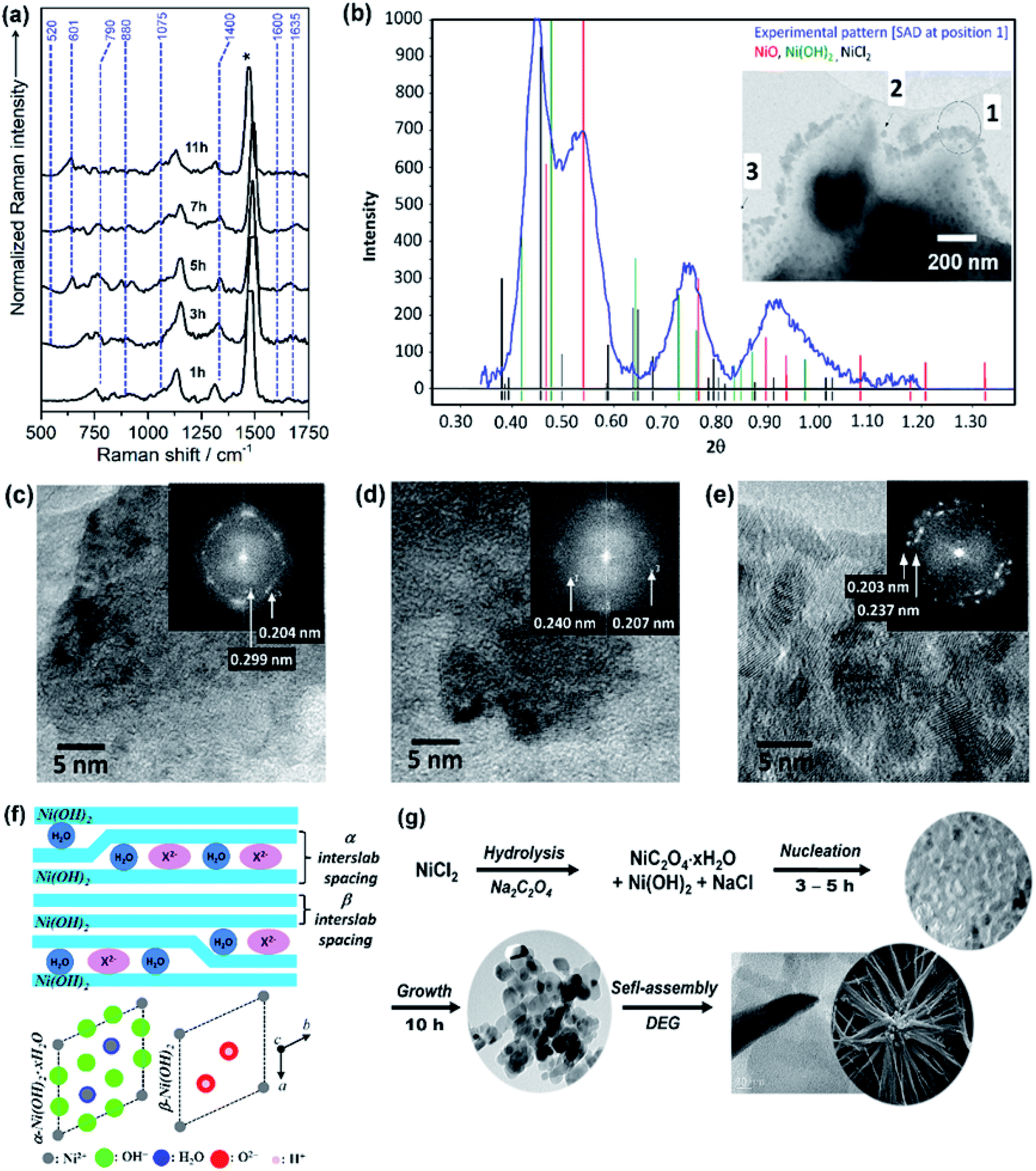 | ||
| Fig. 1 (a) Raman spectra of reaction solution containing intermediates, NiC2O4·xH2O and Ni(OH)2, during the synthesis of NiO NS. (b) The intensity profile of selected area diffraction (SAD) pattern of reaction intermediates (7 h, 180 °C) dried at 150 °C. Inset of panel (b) shows the TEM image for different SAD measurements, in which HRTEM images at position (c) 2 and (d) 3 are recorded. (e) HRTEM image of NiO samples (11 h, 220 °C) annealed at 200 °C. Inset of panel (c–e) shows fast Fourier transform (FFT) images of the corresponding HRTEM images indicating the lattice spacing. (f) A schematic of α/β-interstratification in a single crystal (left) and the idealized crystal structure of α-Ni(OH)2·xH2O and β-Ni(OH)2 represented by unit cell projection (right) adopted from literature.42 (g) Schematic growth and formation mechanism of NiO NS. | ||
The electron micrographs (Fig. 2) compare the morphology of NiO NS to the structures of NiO NP and NiO NF (see Experimental section for synthesis details). NiO NS show a porous surface constituted of 3D networks composed of 3 to 5 μm fibers that are assembled into star-like shapes (Fig. 2a). These fibers are formed by NiO nanoparticles chained up to form quasi-1D structures (inset Fig. 2b). The morphology of NiO NP (Fig. 2c) reveals that the primary nanoparticles also form aggregates. However, compared to NiO NS, the nanoparticle aggregates form a dense and compact surface. The aggregation in both NiO NS and NiO NP is due to the role of DEG during the growth of Ni(OH)2. The aggregates form a compact surface in NiO NP since higher concentration of DEG is used in the synthesis of NiO NP, while formation of porous self-assembled nanoparticles in NiO NS requires a mixture of DEG and water as solvent. Due to the water content during NS synthesis, hydrolysis forming Ni(OH)2 occurs rapidly which breaks aggregation and eventually forms the fiber-based nanostars. NiO NF show characteristic thin flake-like nanostructures (Fig. 2d) which also form a surface with porous flake networks.
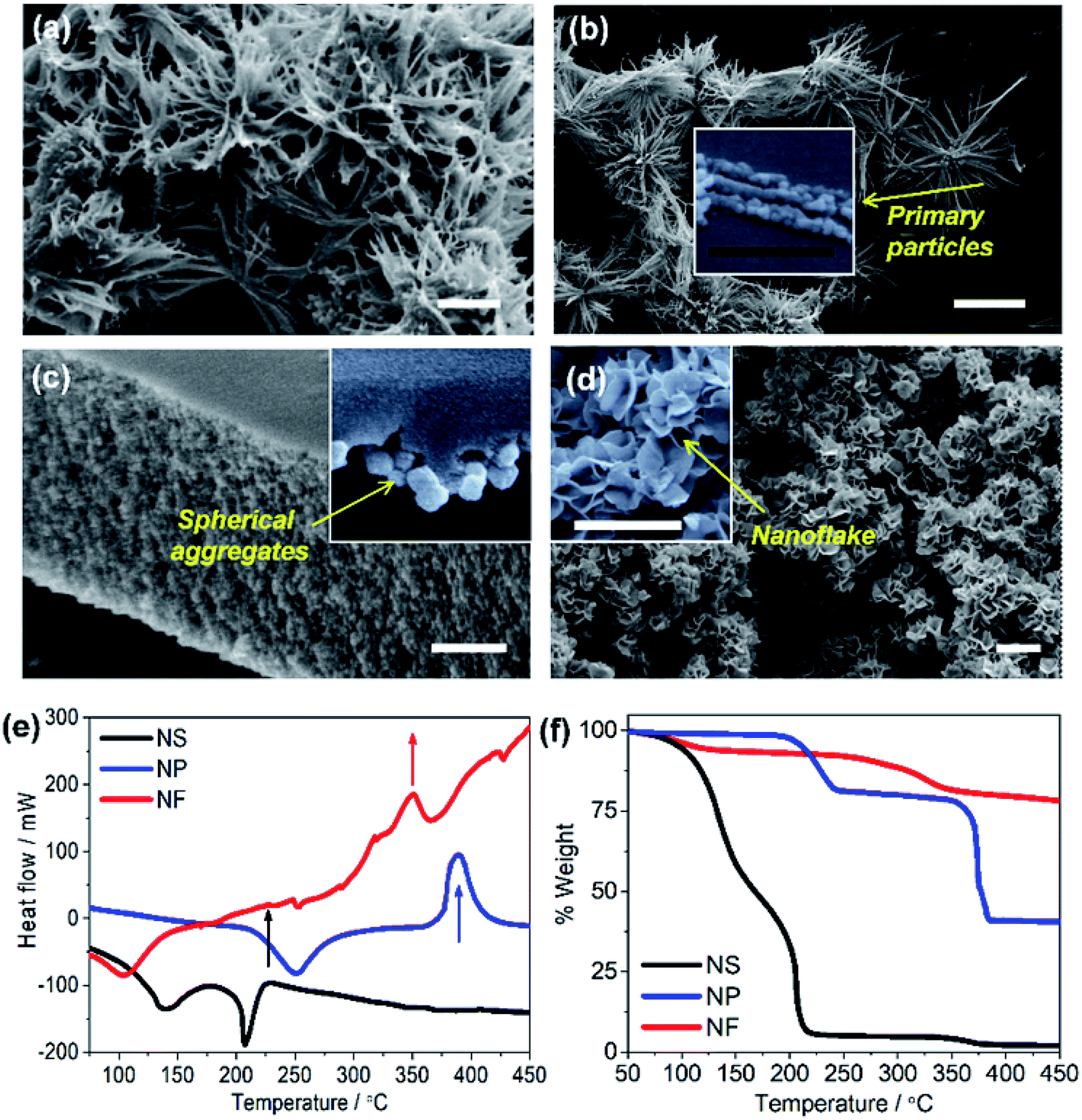 | ||
| Fig. 2 Secondary electron images of (a and b) NiO nanostars (NS), (c) NiO nanoparticles (NP), and (d) NiO nanoflakes (NF). Inset of the figures is enlarged SEM images indicating the primary particles in NiO NS, the aggregation in NiO NP, and the flake structure in NiO NF. The white bar is equal to 1 μm and the black bar is equal to 300 nm. (e) DSC and (f) TGA spectra of NiO NS, NiO NP, and NiO NF measured under N2 atmosphere with a heating rate of 10 K min−1. | ||
Prior to investigating the electronic and microstructural properties of NiO NS, knowledge about the pre-formed NiO, i.e. α-Ni(OH)2 and β-Ni(OH)2, is important to obtain as different polymorphs of Ni(OH)2 might affect the defect characteristics of NiO:42–44 The β-phase possesses an isostructure of the brucite Mg(OH)2 while the α-Ni(OH)2 constitutes stacking β-Ni(OH)2 parallel to ab-plane intercalated by water molecules (see Fig. 1f). A first indication on the formation of either α or β polymorph is provided by thermal analysis, i.e. DSC (Fig. 2d). The first exothermal peak in DSC at 225 °C indicates the transformation of Ni(OH)2 to NiO NS. NiO NP and NiO NF on the other hand are formed upon thermally annealing of Ni(OH)2 at 390 and 350 °C, respectively. The significant weight loss of NiO NS at relatively low temperatures is due to the loss of surface adsorbed water (T ≈ 100–150 °C) which is a characteristic of β-Ni(OH)2: surface water and incorporated water in β-Ni(OH)2 can be completely removed at T ≈ 160 °C.42 In contrast, a notable weight loss starting at higher temperature of 300 °C for either NiO NP and NiO NF indicates that α-Ni(OH)2 are the pre-formed nickel hydroxide for both nanostructures.42 α-Ni(OH)2 is always hydrated by intercalated water, which is intrinsic to their structure (α-Ni(OH)2·xH2O), so that higher temperatures, T ≈ 240–300 °C, are required to remove the water.42,44
Raman spectroscopy is used to further assess the Ni(OH)2 polymorphs preforming NiO (Fig. S3 and S4 in ESI†). Raman spectra of preformed-NiO NS show characteristics of β-Ni(OH)2: Raman peaks at 441, 607, and 900 cm−1.42–44 Raman spectra of preformed-NiO NF and NiO NP exhibit in addition to the features of β-Ni(OH)2 the Raman peaks characteristic for α-Ni(OH)2, i.e. at 1050, 1565, and 3300 cm−1.43–45 Finally, all NiO nanostructures present the typical Raman peaks for cubic NiO single crystals at 419, 509, 875, 1010 and 1562 cm−1.
The microstructural properties of NiO nanostructures are assessed by X-ray diffraction (Fig. 3). The diffraction pattern within the range of diffraction angle between 15 and 70° is assigned to the bunsenite-type of NiO, where peaks at 37.25, 43.29, and 62.91° correspond to the (111), (200), and (200) planes, respectively.46–48 Furthermore, all nanostructures show the (200) crystal plane as the preferred orientation indicating that the resultant NiO nanostructures are formed with stoichiometric ratio. In addition, consistent with the analyses by DSC and Raman scattering, the preformed Ni(OH)2 is dominated by β-Ni(OH)2 for NiO NS, while a mixture of α-Ni(OH)2 and β-Ni(OH)2 is observed as the precursor for NiO NP and NiO NF (Fig. 3 and in ESI†). For NiO NS, HRTEM images (Fig. 3c–e) further corroborate the XRD analysis. The HRTEM of NiO NS annealed at 250 °C (phase transformation temperature) reveal a lattice spacing of 0.207 and 0.241 nm characteristic for the (111) and (200) orientations of bunsenite NiO, respectively.
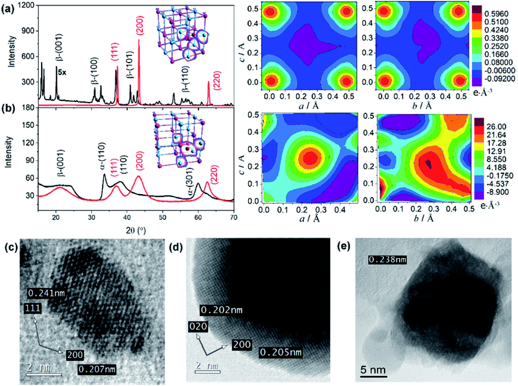 | ||
| Fig. 3 X-ray diffraction pattern of Ni(OH)2 (black) and NiO (red) of (a) NS and (b) NF. The right panel shows the electron density map derived from the Fourier analysis of X-ray diffraction pattern of NiO NS and NiO NF. The Ni and O atoms in the electron density map are placed in the corner of figures (Ni: bottom-left and top-right, while O: top-left and bottom-right). HRTEM images of primary crystallites of NiO NS prepared at (c) 250 °C and (d and e) 450 °C. | ||
A quantitative analysis yields the microstructural properties, i.e. crystallite size, lattice strain and dislocation density. The crystallite size of NiO NS is estimated by the Debye–Scherrer formula49 to 11.5 nm. According to the Stokes-Wilson approximation50 the lattice strain of NiO NS is 0.0034 and the dislocation density of NiO NS amounts to 9.4 1015 lines per m2. Compared to other nanostructures, the lattice strain and dislocation density in NiO NS is lower (see ESI†) indicating a low density of defects. Furthermore, different defects, which are (at least to some extent) characteristic for each of the NiO nanostructures, yield distinct electronic properties, e.g. indicated by the distribution of charge density within the crystal structure as revealed in the 3D (inset of XRD pattern) and 2D Fourier maps (Fig. 3, right panel). As shown, the positive charge density dominates the Fourier maps indicating hole as majority carriers in p-type NiO. For NiO NS, the highest positive charges density (0.59 e Å−3) are largely localized at either O and Ni atoms. A similar charge density distribution is found in NiO NP (Fig. S5 in ESI†) while in NiO NF both high positive (26.0 e Å−3) and negative (−9.1 e Å−3) charge density is delocalized in the space of the unit cells, indicating the possible intercalation of impurities. This is at least plausible when considering the growth of NiO NF predominantly from α-Ni(OH)2. These differences in charge density distribution within the unit cells of NiO might affect its affinity towards binding sensitizers51,52 onto the surface of the photocathode materials (vide infra).
Optical, electrochemical, and physical properties of NiO nanostars
Fig. 4a shows the absorption and emission spectra of NiO NS in comparison to other NiO structures. An absorption band at 385 nm is observed and the energy band gap of NiO NS estimated from Tauc plots, i.e. 3.83 eV, is consistent within the range of NiO optical band gaps reported in literature.51–53 The emission of NiO shows near band edge (NBE) UV emission and deep level (DL) defect related emission in the visible range (inset of Fig. 4a). The NBE emission stems from direct exciton recombination. DL emission originates from either the radiative recombination either between a photo-generated hole and an electron occupying the nickel interstitial (Nii, λem ≈ 420 nm) and vacancy (VNi2−, λem ≈ 460 nm) or between an electron in conduction band and a photo-generated trapped hole occupying oxygen vacancy (VO2+, λem ≈ 527 nm) and interstitial (Oi, λem ≈ 585 nm).53–55 The Oi and VO2+ defects are thus considered shallow and deep trap states, respectively. These traps determine the charge transport in NiO and act as recombination centers. For NiO NS, it is clear that the relative emission intensity originating from VO2+ and Oi defects is the lowest among all investigated NiO nanostructures. | ||
| Fig. 4 (a) UV/vis absorption and emission (inset) of NiO NS, NiO NP, and NiO NF. Emission spectra were recorded upon excitation at 310 nm. (b) Cyclic voltammogramms of NiO recorded after 20 cycles of measurement at scan rate of 100 mV s−1 using 0.2 M KCl as the supporting electrolyte and 0.01 M KH2PO4 and 0.01 M K2HPO4 as the buffer. (c) The trapping states densities originating from bulk traps (black) and surface traps (blue) of NiO NF, NiO NP, and NiO NS. The trapping state density distribution is derived from the open-circuit voltage decay (OCVD) measurement (Fig. S11 in ESI†). | ||
The cyclic voltammogramm of NiO NS (Fig. 4b) shows two oxidation peaks at 0.58 and 1.01 V (vs. Ag/AgCl) which can be attributed to Ni2+/Ni3+ and Ni3+/Ni4+, respectively. The diverging current above 1.2 V is due oxygen evolution (2OH− → H2O + 1/2O2 + 2e−).56 The electrochemical data is used to assess the basic functionality of the NiO nanostructures to serve as material in a dye-sensitized photocathode (vide infra). The driving force for hole injection ΔGinj = e[EVB(NiO) − {E0–0(S*) + E(S/S−)}] is estimated by taking into account the flat band potential (Fig. S8, in ESI†).57,58 The flat band potential of NiO NS is found at 0.52 V vs. Ag/AgCl at pH 7 which is comparable to the value of 0.47 V vs. Ag/AgCl, which is reported in literature.58 When organic dye P1 is considered as photosensitizer (E0–0 (S*) = 2.25 eV, and E(S/S−) = −0.767 V vs. NHE),17 NiO NS yield ΔGinj = −0.764 eV. This estimation presents a preliminary indication that NiO NS are suitable for the preparation of photocathodes. Furthermore, the trapping states in NiO, which act as recombination centers and affect the hole mobility in the material, are evaluated using the open circuit voltage decay (OCVD).36 The density of trapping states in NiO (Fig. 4d) generally shows a non-exponential VB tail due to the complex band structure with multiple valence bands (3d band of Ni2+ and 2p band of O2−).31,59 The density of bulk traps (BTs, in Fig. 4c) is similar for all investigated NiO nanostructures. These bulk traps allow release of a trapped hole to the valence band at room temperature. Surface traps (STs) on the contrary release trapped holes to either valence band or other acceptor species, for example, the oxidized species in electrolyte. In a good agreement with the minimum VO2+ and Oi defect emission in NiO NS, the corresponding density of STs in NiO NS is also the lowest of amongst all investigated nanostructures, reflecting the minimized density of recombination centres.
As a next step towards evaluating different NiO nanostructures as materials for photocathodes, their sensitization by various molecular photosensitizer is discussed: Table 1 summarizes the dye loading and other important physical properties of the photocathodes. BET measurement shows that the specific surface area of NiO NS is moderate with 44.9 m2 g−1. The N2 isotherm adsorption and desorption curve of NiO NS (Fig. S10 in ESI†) indicates the mesoporous character of the semiconductor material (pore diameter between 2 and 50 nm). This observation is supported by BJH (Barret–Joyner–Halenda) analysis, which reveals a peak pore radius of NiO NS of 5.7 nm. The resultant pore volume of the NS, 0.064 cc g−1, is the largest amongst the different NiO nanostructures compared. Grafting of the organic dye P1 with carboxylic anchoring group (Fig. 5) on the NiO nanostructures yields dye loading of 41.0, 15.1, and 7.9 nmol cm−2 for NiO NS, NiO NP, and NiO NF, respectively (obtained from the dye desorption test, see Experimental section). Despite the fact that NiO NF displays a higher surface area, the dye-loading does not scale with the surface area (see Table 1): NiO NS exhibit three (vs. NiO NP) or five times (vs. NiO NF) higher dye-loading irrespective of the dye's specific anchoring groups (i.e. Copper complex bearing pyridine anchoring group (Cu1), RuII complex bearing phosphonic acid (Ru1) and methyl-ester (Ru2) anchoring group, see Table 1), which is consequently profitable for current generation when used as photocathodes.
| NiO | Efb (vs. Ag/AgCl)/V | S/m2 g−1 | rS/nm | VS/cc g−1 | d/μm | Dye-loading/nmol cm−2 | |||
|---|---|---|---|---|---|---|---|---|---|
| –COOH (P1) | –C5H4N (Cu1) | –POOH (Ru1) | –COOH (Ru2) | ||||||
| NS | 0.51 | 44.9 | 5.7 | 0.064 | 1.62 | 41.0 | 3.1 | 18.3 | 20.6 |
| NP | 0.44 | 21.2 | 4.7 | 0.050 | 1.05 | 15.1 | 1.0 | 8.3 | 12.7 |
| NF | 0.36 | 120.9 | 2.1 | 0.056 | 2.27 | 7.9 | 0.7 | 2.0 | 6.9 |
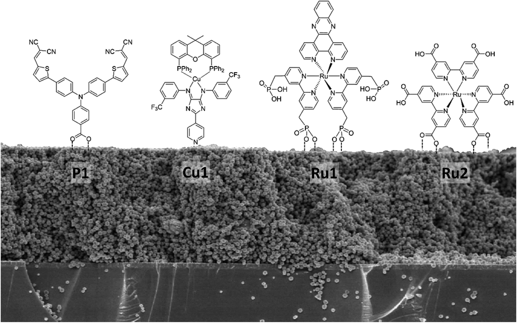 | ||
| Fig. 5 Different molecular structures of photosensitizers bearing different anchoring groups used for dye-loading studies on NiO nanostructures. | ||
This seemingly contradictory behaviour can be related to the microstructure and electronic properties discussed earlier. The different dye-loading capacity can be rationalized by the different affinity of NiO surface toward different anchoring groups of dye photosensitizers.60–64 As revealed in charge density maps (Fig. 3a), the positive charge density of NiO NS is mainly localized on either the O or Ni atom and hence, it is advantageous since binding modes of phosphonic and carboxylic acid anchoring group toward NiO surface are determined by the formation of strong P–O–Ni and C–O–Ni covalent bonds, respectively.52–54 Electrostatic interaction between pyridine anchoring moiety and non-polar plane (100) of NiO may occur for sensitization although the binding strength is lower than the interaction between either carboxylic or phosphonic acid and NiO, and hence, it results in a lower dye-loading compared with other complexes.60,61
NiO NS-based dye-sensitized solar cells
To evaluate the performance of the different NiO nanostructures in functional photocathodes, the RuII complex (Ru2), the organic dyes P1 and Coumarin 343 (C343) were used as photosensitizers in DSSCs. The photocurrent density–voltage (J–V) curves and impedance characteristics of DSSCs using Ru2 are shown in Fig. 6 and summarized in Table 2. In addition, photoelectrochemical properties of DSSCs using P1 and C343 are summarized in Table S1 (in ESI†). The J–V curves reveal that the PCE of NiO NS-based DSSCs using the RuII complex (VOC = 0.129 V, JSC = 3.72 mA cm−2, FF = 0.32, η = 0.144%) is superior to those of NiO NF-based DSSC (VOC = 0.141 V, JSC = 0.21 mA cm−2, FF = 0.33, η = 0.010%) and NiO NP-based DSSCs (VOC = 0.125 V, JSC = 0.49 mA cm−2, FF = 0.31, η = 0.018%). Irrespective of the molecular photosensitizer, NiO-NS photocathodes yield higher efficiencies compared to NiO NF and NiO NP. The performance differences between various NiO nanostructures can be attributed to the different dye loadings (see Table 1). The increased P1-loading on NiO NS leads to the highest photocurrent generation in the respective DSSCs. However, the photocurrent does not scale linearly with the dye loading on the NiO structures. This indicates that another factor contributes to the superior performance of the NiO-NS DSSCs: the reduced surface trap density in NiO NS might reduce non-geminate recombination reactions at the photocathode surface.54,68 This reduced recombination leads to a more stable charge separation at the dye-sensitized NiO interface yielding improved performance parameters as reflected in the molecular electron transfer density (Γ summarized in Tables 2 and S1 in ESI†). It is also worth mentioning that the NiO NS with P1 as sensitizer (η = 0.145%) performs on par with the best NiO DSSCs previously reported, i.e. PCE of 0.15% in DSSCs using P1-sensitized F108 polymer-templated NiO films and I3−/I− redox couple as electrolyte.63 Furthermore, the PCE of NiO NS-based DSSCs are superior to other DSSCs, in which NiO photocathodes are prepared using commercial NiO paste or prepared using diblock copolymer template, reported in other literature, i.e. maximum PCE of 0.079–0.116%.54–68 | ||
| Fig. 6 (a) The J–V curves of DSSC utilizing various NiO photocathodes, i.e. NS, NP, and NF, sensitized with Ru2 in acetonitrile. (b) The impedance spectra, including Nyquist (top) and Bode plots (bottom), of DSSCs utilizing various NiO photocathodes in the presence of Iodine-based electrolyte and under irradiation. (c) Equivalent circuit model for fitting the electrochemical impedance data. | ||
| NiO structure | EIS | OCVD | J–V | |||||||
|---|---|---|---|---|---|---|---|---|---|---|
| Rrec/kOhm | Ln/L | τVB/s | τ1/s (A1) | τ2/s (A2) | Jsc/mA cm−2 | Voc/V | FF | η/% | Γ/mA cm−3 | |
| NS | 5.23 | 1.89 | 0.37 | 1.8 (0.59) | 17 (0.41) | 3.95 | 0.121 | 0.31 | 0.145 | 0.81 |
| NP | 2.56 | 1.57 | 0.26 | 2.8 (0.36) | 21 (0.64) | 0.64 | 0.115 | 0.32 | 0.023 | 0.17 |
| NF | 2.30 | 1.03 | 0.21 | 0.5 (0.34) | 9.4 (0.66) | 0.34 | 0.156 | 0.28 | 0.015 | 0.14 |
The performance of DSSCs using different NiO nanostructures is further evaluated by electrochemical impedance spectroscopy (EIS, Fig. 6b). According to an impedance study on dye-sensitized NiO solar cells by Wu and co-workers,14,26 the Nyquist plots (Fig. 6b) show two semicircles attributed to (i) electron transfer at the NiO/dye/electrolyte interface and within the NiO film (charge transfer resistance R2 ∼ Rct, bigger semicircle in the frequency range of 1 to 103 Hz) and (ii) electron ejection at the counter electrode/electrolyte interface and the transport in the electrolyte (R1 ∼ Rtr, smaller semicircle in the frequency range of 103 to 105 Hz). By fitting an equivalent circuit model (Fig. 6c)18 to the impedance data the recombination resistance (Rrec), the effective diffusion length (Ln/L), and the hole lifetime (τ) can be quantified. The thus obtained values are summarized in Table 2.
NiO NS show two times higher recombination resistance than other nanostructures, i.e. the overall interfacial recombination is minimized in NiO NS. The effective diffusion length (Ln/L = 1.89), which is highest in NiO NS, indicates that NiO NS electrodes can be prepared with a thickness of up to 1.9 times higher than the thickness of the electrodes used in this study (ca. 1.5 μm) without affecting the charge collection efficiency. The higher ratio Ln/L also reflects the increased hole transport within NiO NS electrodes. Finally, the hole lifetime (τVB) in NiO NS, which characterizes the recombination rate between the non-geminate holes in the VB edge and the extended band gap with the acceptor species, is the longest of all investigated structures.
Photoelectrochemical activity of NiO NS photocathode
Finally, the photoelectrochemical activity of the different NiO films was assessed under fully aqueous conditions, pertinent for DSPEC applications. The organic push–pull dye T1 was employed to sensitize the films and chronoamperometric measurements were recorded under chopped-light irradiation (400–800 nm filtered Xe lamp light; 100 mW cm−2) in aqueous sodium acetate buffer pH 4.5 as the electrolyte, in the presence of the irreversible electron acceptor [Co(NH3)5Cl]Cl2 (IEA, see Fig. 7a), as we previously reported for a related system.29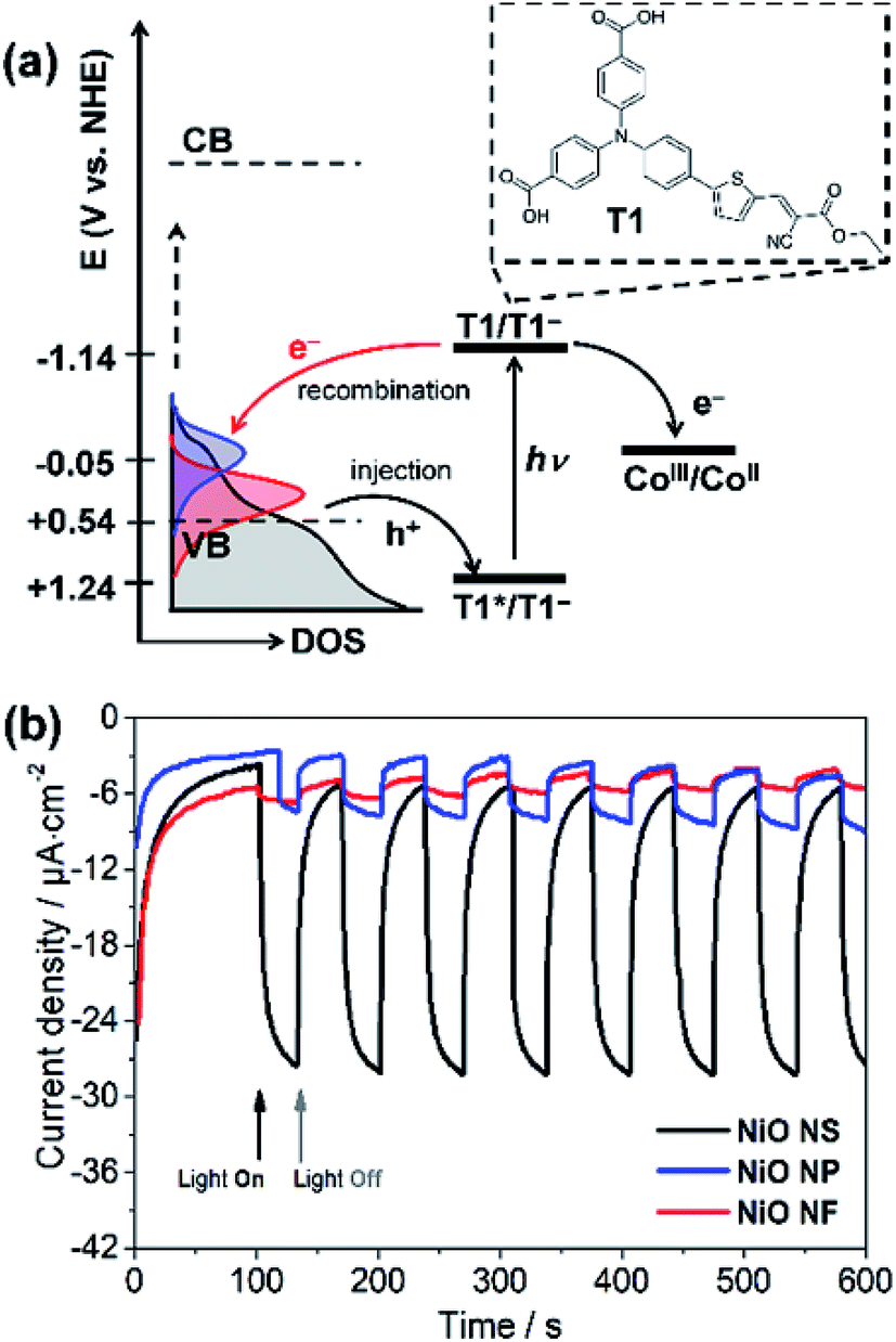 | ||
| Fig. 7 (a) Schematic representation of the T1-sensitized NiO photocathodes working principle. (b) Cathodic photocurrent densities recorded for various NiO nanostructures in the presence of [Co(NH3)5Cl]Cl2 (20 mM) as IEA. The measurements were carried out in acetate buffer 0.1 M (pH 4.5) at an applied potential of 0 V vs. Ag/AgCl. | ||
Cathodic photocurrents were measured under visible light irradiation (Fig. 7b) likely associated with the reductive quenching mechanism shown in Fig. 7a: upon photoexcitation of T1, a hole is injected from its excited state to the VB of NiO creating a charge-separated states between radical anion T1− immobilized on NiO and photoinjected hole (T1−|NiO(h+)). Hole injection was indeed previously shown to occur on the subpicosesond timescale for F108-templated NiO films sensitized with T1.39 Subsequently, the CoIII irreversible electron acceptor present in solution is reduced by thermal electron transfer from T1−, thus regenerating T1. The net photocurrent is determined by the efficiencies of hole injection, dye regeneration, and more importantly the stability of charge-separated states.9–11 According to literature,61 the Gibbs free energies for both hole injection into the NiO valence band (ΔGing) and dye regeneration (ΔGreg) are exergonic. The driving force ΔGreg is estimated to −1.09 V by ΔGreg = e[E(T1/T1−) − E(CoIII/CoII)], where E(T1/T1−) and E(CoIII/CoII) are −1.77 and −0.68 V vs. Fc+/0, respectively. However, the driving force of hole injection can vary because the morphology dependent VB potential. The estimated ΔGinj = e[EVB(NiO) − {E(T1/T1−) + E0–0}] for NiO NS is −0.27 eV enabling efficient hole injection into NiO NS.
Fig. 7b shows the photocurrents recorded using different NiO photocathodes. The photocathode based on NiO NS generates photocurrents of 23 μA cm−2. The significant drop in photocurrent when comparing NiO NF to NS (drop of more than 1700%) can be associated with the inferior dye-loading: 17.4 nmol cm−2 of the dye are chemisorbed on NiO NS, i.e. the loading is about 800% higher than in NiO NF (1.9 nmol cm−2). Other factors that might also contribute the superior performance of the NiO NS cathode are more efficient hole injection and a higher charge collection efficiency due to increased hole mobility. The photocurrent in the NiO NS-based DSPEC performs comparably to commercially available NiO films with an average photocurrent of 30 μA cm−2 (Fig. S12† in ESI†).
Conclusions
A facile wet chemical synthetic route to synthesize mesoporous bunsenite-NiO nanostars (NS) is presented. Compared to other structures, including compact NiO nanoparticles (NP) and porous NiO nanoflakes (NF), which are formed upon transformation of a mixture of α- and β-Ni(OH)2, the resulting NiO NS are formed from β-Ni(OH)2. The type of Ni(OH)2 polymorph preforming NiO is found to significantly control its functionality toward molecular sensitizer. NiO NS shows versatile properties, i.e. high optical band gap, low defect concentrations, high surface area and pore volume, and suitable electron density distribution, enable functionalization with dyes bearing various anchoring groups. When used as photocathode, NiO NS studied here also show a comparably higher efficiency in DSSCs and higher cathodic photocurrent generation in DSPECs than similar systems reported in literature. Modification of mesoporous structure of NiO NS based on the current synthetic route is possible by varying the ratio between the water and DEG as the hydrolysis and self-assembly agent, respectively, for further investigation on the correlation between pore structure and photocathode performance.Conflicts of interest
There are no conflicts to declare.Acknowledgements
We thank the Deutscher Akademischer Austauschdienst (DAAD) for PhD Scholarship for RAW. Financial support by the Fonds der Chemischen Industrie is gratefully acknowledged. We also thank Dr Martin Schulz for providing Cu(I) complex for dye-loading experiments. The co-authors (MR and MS) thank Deutsche Forschungsgemeinschaft (DFG) for financial support (RE 1261/19-1).References
- A. Hagfeldt, G. Boschloo, L. Sun, L. Kloo and H. Pettersson, Chem. Rev., 2010, 110, 6595–6663 CrossRef CAS PubMed.
- S. Mathew, A. Yella, P. Gao, R. Humphry-baker, B. F. E. Curchod, N. Ashari-Astani, I. Tavernelli, U. Rothlisberger, M. K. Nazeeruddin and M. Grätzel, Nat. Chem., 2014, 6, 242–247 CrossRef CAS PubMed.
- M. Grätzel, J. Photochem. Photobiol., C, 2003, 4(2), 145–153 CrossRef.
- J. He, H. Lindström, A. Hagfeldt and S.-E. Lindquist, J. Phys. Chem. B, 1999, 103, 8940–8943 CrossRef CAS.
- F. Odobel and Y. Pellegrin, J. Phys. Chem. Lett., 2013, 4, 2551–2564 CrossRef CAS.
- H. Choi, T. Hwang, S. Lee, S. Nam, J. Kang, B. Lee and B. Park, J. Power Sources, 2015, 274, 937–942 CrossRef CAS.
- A. Nattestad, A. J. Mozer, M. K. R. Fischer, Y.-B. Cheng, A. Mishra, P. Büerle and U. Bach, Nat. Mater., 2009, 9, 31–35 CrossRef PubMed.
- N. Queyriaux, N. Kaeffer, A. Morozan, M. Chavarot-Kerlidou and V. Artero, J. Photochem. Photobiol., C, 2015, 25, 90–105 CrossRef CAS.
- M. K. Brennaman, J. R. Dillon, L. A. Libabaei, M. K. Gish, C. J. Dares, D. L. Ashford, R. L. House, G. J. Meyer, J. M. Papanikolas and T. J. Meyer, J. Am. Chem. Soc., 2016, 138, 13085–13102 CrossRef CAS PubMed.
- D. L. Ashford, M. K. Gish, A. K. Vannucci, M. K. Brennaman, J. L. Templeton, J. M. Papanikolas and T. J. Meyer, Chem. Rev., 2015, 115, 13006–13049 CrossRef CAS PubMed.
- E. A. Gibson, Chem. Soc. Rev., 2017, 46, 6194–6209 RSC.
- G. Sahara, R. Abe, M. Higashi, T. Morikawa, K. Maeda, Y. Ueda and O. Ishitani, Chem. Commun., 2015, 51, 10722–10725 RSC.
- A. Nattestad, A. J. Mozer, M. K. R. Fischer, Y. B. Cheng, A. Mishra, P. Bauerle and U. Bach, Nat. Mater., 2010, 9, 31–35 CrossRef CAS.
- A. K. Click, D. R. Beauchamp, Z. Huang, W. Chen and Y. Wu, J. Am. Chem. Soc., 2016, 138, 1174–1179 CrossRef PubMed.
- A. K. Click, D. R. Beauchamp, B. R. Garrett, Z. Huang, M. C. Hadad and Y. Wu, Phys. Chem. Chem. Phys., 2014, 16, 26103–26111 RSC.
- X. L. Zhang, Z. Zhang, D. Chen, P. Bauerle, U. Bach and Y. B. Cheng, Chem. Commun., 2012, 48, 9885–9887 RSC.
- E. A. Gibson, M. Awais, D. Dini, D. P. Dowling, M. T. Pryce, J. G. Vos, G. Boschloo and A. Hagfeldt, Phys. Chem. Chem. Phys., 2013, 15, 2411–2420 RSC.
- P. Qin, M. Linder, T. Brinck, G. Boschloo, A. Hagfeldt and L. Sun, Adv. Mater., 2009, 21, 2993–2996 CrossRef CAS.
- C. J. Flynn, E. E. Oh, S. M. McCullough, R. W. Call, C. L. Donley, R. Lopez and J. F. Cahoon, J. Phys. Chem. C, 2014, 118, 14177–14184 CrossRef CAS.
- A. Natastad, X. Zhang, U. Bach and Y.-B. Cheng, J. Photonics Energy, 2011, 1, 011103 CrossRef.
- F. Odobel, L. Le Pleux, Y. Pellegrin and E. Blart, Acc. Chem. Res., 2010, 43(8), 1063–1071 CrossRef CAS PubMed.
- C. D. Windle, H. Kumagai, M. Higashi, R. Brisse, S. Bold, B. Jousselme, M. Chavarot-Kerlidou, K. Maeda, R. Abe, O. Ishitani and V. Artero, J. Am. Chem. Soc., 2019, 141(24), 9593–9602 CrossRef CAS PubMed.
- M. Yu, G. Natu, Z. Ji and Y. Wu, J. Phys. Chem. Lett., 2012, 3, 1074–1078 CrossRef CAS PubMed.
- M. Yu, T. I. Draskovic and Y. Wu, Phys. Chem. Chem. Phys., 2014, 16, 5026–5033 RSC.
- O. Langmar, C. R. Ganivet, A. Lennart, R. D. Costa, G. de la Torre, T. Torres and D. M. Guldi, Angew. Chem., 2015, 127, 7798–7802 CrossRef.
- C. C. Mercado, A. Zakutayev, K. Zhu, C. J. Flynn, J. F. Cahoon and A. J. Nozik, J. Phys. Chem. C, 2014, 118, 25340–25349 CrossRef CAS.
- S. M. McCullough, C. J. Flynn, C. C. Mercado, A. J. Nozik and J. F. Cahoon, J. Mater. Chem. A, 2015, 3, 21990–21994 RSC.
- D. Dini, Y. Halpin, J. G. Vos and E. A. Gibson Coord, Chem. Rev., 2015, 304–305, 179–201 CAS.
- L. Lepleux, B. Chavillon, Y. Pellegrin, E. Blart, L. Cario, S. Jobic and F. Odobel, Inorg. Chem., 2009, 48, 8245–8250 CrossRef CAS PubMed.
- H. Yang, G. H. Guai, C. Guo, Q. Song, S. P. Jiang, Y. Wang, W. Zhang and C. M. Li, J. Phys. Chem. C, 2011, 115, 12209–12215 CrossRef CAS.
- L. D'Amario, L. J. Antila, B. P. RImgard, G. Boschloo and L. Hammarström, J. Phys. Chem. Lett., 2015, 6, 779–783 CrossRef PubMed.
- M. Bräutigam, J. Kübel, M. Schulz, J. G. Vos and B. Dietzek, Phys. Chem. Chem. Phys., 2015, 17, 7823–7830 RSC.
- N. Queyriaux, R. A. Wahyuono, J. Fize, C. Gablin, M. Wächtler, E. Martinez, D. Leonard, B. Dietzek, V. Artero and M. Chavarot-Kerlidou, J. Phys. Chem. C, 2017, 121(11), 5891–5904 CrossRef CAS PubMed.
- M. Schulz, N. Hagmeyer, F. Wehmeyer, J. G. Vos and B. Dietzek, ChemRxiv, 2019 DOI:10.26434/chemrxiv.7229054.v2.
- R. A. Wahyuono, B. Schulze, M. Rusu, M. Wächtler, J. Dellith, M. Seyring, M. Rettenmayr, J. Plentz, A. Ignaszak, U. S. Schubert and B. Dietzek, ChemPlusChem, 2016, 81(12), 1281–1291 CrossRef.
- A. Zaban, M. Greenshtein and J. Bisquert, ChemPhysChem, 2003, 4, 859–864 CrossRef CAS PubMed.
- J. Bisquert, A. Zaban, M. Greenshtein and I. Mora-Sero, J. Am. Chem. Soc., 2004, 126, 13550–13559 CrossRef CAS.
- J. Massin, M. Bräutigam, N. Kaeffer, N. Queyriaux, M. J. Field, F. H. Schacher, J. Popp, M. Chavarot-Kerlidou, B. Dietzek and V. Artero, Interface Focus, 2015, 5, 20140083 CrossRef.
- J. Massin, M. Bräutigam, S. Bold, M. Wächtler, M. Pavone, A. B. Munoz-Garcia, B. Dietzek, V. Artero and M. Chavarot-Kerlidou, J. Phys. Chem. C, 2019, 123(28), 17176–17184 CrossRef CAS.
- C. Xu, G. Xu and G. Wang, J. Mater. Sci., 2002, 38, 779–782 CrossRef.
- R. I. Bickley, H. G. M. Edwards and S. J. Rose, J. Mol. Struct., 1991, 243, 341–350 CrossRef CAS.
- D. S. Hall, D. J. Lockwood, C. Bock and B. R. MacDougall, Proc. R. Soc., 2014, 471, 20140792, DOI:10.1098/rspa.2014.0792.
- D. S. Hall, D. J. Lockwood, S. Poirier, C. Bock and B. R. MacDougall, J. Phys. Chem. A, 2012, 116, 6771–6784 CrossRef CAS.
- D. S. Hall, D. J. Lockwood, S. Poirier, C. Bock and B. R. MacDougall, ACS Appl. Mater. Interfaces, 2014, 6(5), 3141–3149 CrossRef CAS.
- R. E. Dietz, G. I. Parisot and A. E. Meixner, Phys. Rev. B: Solid State, 1971, 4, 2302–2310 CrossRef.
- Z. Zhang, Y. Zhao and M. Zhu, Appl. Phys. Lett., 2006, 88, 033101 CrossRef.
- B. Subramanian, M. M. Ibrahim, V. Senthilkumar, K. R. Murali, V. S. Vidhya, C. Sanjeeviraja and M. Jayachandran, Phys. B, 2008, 403, 4104–4110 CrossRef CAS.
- C. A. Ventrice Jr., Th. Betrams, H. Hannemann, A. Brodde and H. Neddermeyer, Phys. Rev. B: Condens. Matter Mater. Phys., 1994, 49, 5773–5776 CrossRef.
- B. D. Cullity. Elements of X-ray Diffraction, 2nd edn, Addison-Wesley Company, USA, 1978 Search PubMed.
- R. Vinodkumar, K. J. Lethy, P. R. Arunkumar, R. R. Krishnan, N. V. Pillai, V. P. M. Pillai and R. Philip, Mater. Chem. Phys., 2010, 121, 406–413 CrossRef CAS.
- L. G. Devi and S. G. Kumar, Appl. Surf. Sci., 2012, 261, 137–146 CrossRef CAS.
- Y. He, O. Dulub, H. Cheng, A. Selloni and U. Diebold, Phys. Rev. Lett., 2009, 102, 106105 CrossRef.
- A. C. Gandhi and S. Y. Wu, Nanomaterials, 2017, 7, 231 CrossRef PubMed.
- L. Le Pleux, B. Chavillon, Y. Pellegrin, E. Blart, L. Carlo, S. Jobic and F. Odobel, Inorg. Chem., 2009, 48(17), 8245–8250 CrossRef CAS PubMed.
- K. W. Wulser, B. P. Hearty and M. A. Langell, Phys. Rev. B: Condens. Matter Mater. Phys., 1992, 46(15), 9724 CrossRef CAS PubMed.
- G. Boschloo and A. Hagfeldt, J. Phys. Chem. B, 2001, 105, 3039 CrossRef CAS.
- G. Natu, P. Hasin, Z. Huang, Z. Ji, M. He and Y. Wu, ACS Appl. Mater. Interfaces, 2012, 4, 5922–5929 CrossRef CAS.
- K. Nakaoka, J. Ueyama and K. Ogura, J. Electroanal. Chem., 2004, 571, 93–99 CrossRef CAS.
- K. W. Wulser, B. P. Hearty and M. A. Langell, Phys. Rev. B: Condens. Matter Mater. Phys., 1992, 46(15), 9724 CrossRef CAS PubMed.
- J. Cui, J. Lu, X. Xu, K. Cao, Z. Wang, G. Alemu, H. Yuang, Y. Shen, J. Xu, Y. Cheng and M. Wang, J. Phys. Chem. C, 2014, 118(30), 16433 CrossRef CAS.
- B. Jin, W. Wu, X. Zhang, F. Guo, Q. Zhang and J. Hua, Chem. Lett., 2013, 42(10), 1271 CrossRef CAS.
- L. Zhang and J. M. Cole, ACS Appl. Mater. Interfaces, 2015, 7, 3427–3455 CrossRef CAS PubMed.
- L. Li, E. A. Gibson, P. Qin, G. Boschloo, M. Gorlov, A. Hagfeldt and L. Sun, Adv. Mater., 2010, 22, 1759 CrossRef CAS PubMed.
- Y. M. Klein, N. Marinakis, E. C. Constable and C. E. Housecroft, Crystals, 2018, 8, 389 CrossRef.
- N. Marinakis, C. Wobil, E. C. Constable and C. E. Housecroft, Polyhedron, 2018, 140, 122–128 CrossRef CAS.
- M. Bonomo, A. Di Carlo, R. Centore, D. Dini and A. Carella, Sol. Energy, 2018, 169, 237–241 CrossRef CAS.
- E. Sheibani, L. Zhang, P. Liu, B. Xu, E. Mijangos, G. Boschloo, A. Hagfeldt, L. Hammarström, L. Kloo and H. Tian, RSC Adv., 2016, 6, 18165–18177 RSC.
- C. J. Wood, G. H. Summers, C. A. Clark, N. Kaeffer, M. Braeutigam, L. R. Carbone, L. D'Amario, K. Fan, Y. Farré, S. Narbey, F. Oswald, L. A. Stevens, C. D. J. Permenter, M. W. Fay, A. La Torre, C. E. Snape, B. Dietzek, D. Dini, L. Hammarström, Y. Pellegrin, F. Odobel, L. Sun, V. Artero and E. A. Gibson, Phys. Chem. Chem. Phys., 2016, 18, 10727–10738 RSC.
Footnote |
| † Electronic supplementary information (ESI) available. See DOI: 10.1039/c9ra08785k |
| This journal is © The Royal Society of Chemistry 2019 |